CN100456209C - Power Management for Integrated Graphics Devices - Google Patents
Power Management for Integrated Graphics Devices Download PDFInfo
- Publication number
- CN100456209C CN100456209C CNB03816213XA CN03816213A CN100456209C CN 100456209 C CN100456209 C CN 100456209C CN B03816213X A CNB03816213X A CN B03816213XA CN 03816213 A CN03816213 A CN 03816213A CN 100456209 C CN100456209 C CN 100456209C
- Authority
- CN
- China
- Prior art keywords
- graphics
- frequency
- circuit
- clock signal
- idle
- Prior art date
- Legal status (The legal status is an assumption and is not a legal conclusion. Google has not performed a legal analysis and makes no representation as to the accuracy of the status listed.)
- Expired - Fee Related
Links
Images


Classifications
-
- G—PHYSICS
- G06—COMPUTING OR CALCULATING; COUNTING
- G06F—ELECTRIC DIGITAL DATA PROCESSING
- G06F1/00—Details not covered by groups G06F3/00 - G06F13/00 and G06F21/00
- G06F1/26—Power supply means, e.g. regulation thereof
- G06F1/32—Means for saving power
-
- G—PHYSICS
- G06—COMPUTING OR CALCULATING; COUNTING
- G06F—ELECTRIC DIGITAL DATA PROCESSING
- G06F1/00—Details not covered by groups G06F3/00 - G06F13/00 and G06F21/00
- G06F1/26—Power supply means, e.g. regulation thereof
- G06F1/32—Means for saving power
- G06F1/3203—Power management, i.e. event-based initiation of a power-saving mode
- G06F1/3206—Monitoring of events, devices or parameters that trigger a change in power modality
- G06F1/3228—Monitoring task completion, e.g. by use of idle timers, stop commands or wait commands
-
- G—PHYSICS
- G06—COMPUTING OR CALCULATING; COUNTING
- G06F—ELECTRIC DIGITAL DATA PROCESSING
- G06F1/00—Details not covered by groups G06F3/00 - G06F13/00 and G06F21/00
- G06F1/26—Power supply means, e.g. regulation thereof
- G06F1/32—Means for saving power
- G06F1/3203—Power management, i.e. event-based initiation of a power-saving mode
- G06F1/3206—Monitoring of events, devices or parameters that trigger a change in power modality
- G06F1/3215—Monitoring of peripheral devices
-
- G—PHYSICS
- G06—COMPUTING OR CALCULATING; COUNTING
- G06F—ELECTRIC DIGITAL DATA PROCESSING
- G06F1/00—Details not covered by groups G06F3/00 - G06F13/00 and G06F21/00
- G06F1/26—Power supply means, e.g. regulation thereof
- G06F1/32—Means for saving power
- G06F1/3203—Power management, i.e. event-based initiation of a power-saving mode
- G06F1/3234—Power saving characterised by the action undertaken
- G06F1/324—Power saving characterised by the action undertaken by lowering clock frequency
-
- G—PHYSICS
- G06—COMPUTING OR CALCULATING; COUNTING
- G06F—ELECTRIC DIGITAL DATA PROCESSING
- G06F1/00—Details not covered by groups G06F3/00 - G06F13/00 and G06F21/00
- G06F1/26—Power supply means, e.g. regulation thereof
- G06F1/32—Means for saving power
- G06F1/3203—Power management, i.e. event-based initiation of a power-saving mode
- G06F1/3234—Power saving characterised by the action undertaken
- G06F1/325—Power saving in peripheral device
-
- G—PHYSICS
- G06—COMPUTING OR CALCULATING; COUNTING
- G06F—ELECTRIC DIGITAL DATA PROCESSING
- G06F1/00—Details not covered by groups G06F3/00 - G06F13/00 and G06F21/00
- G06F1/26—Power supply means, e.g. regulation thereof
- G06F1/32—Means for saving power
- G06F1/3203—Power management, i.e. event-based initiation of a power-saving mode
- G06F1/3234—Power saving characterised by the action undertaken
- G06F1/3296—Power saving characterised by the action undertaken by lowering the supply or operating voltage
-
- Y—GENERAL TAGGING OF NEW TECHNOLOGICAL DEVELOPMENTS; GENERAL TAGGING OF CROSS-SECTIONAL TECHNOLOGIES SPANNING OVER SEVERAL SECTIONS OF THE IPC; TECHNICAL SUBJECTS COVERED BY FORMER USPC CROSS-REFERENCE ART COLLECTIONS [XRACs] AND DIGESTS
- Y02—TECHNOLOGIES OR APPLICATIONS FOR MITIGATION OR ADAPTATION AGAINST CLIMATE CHANGE
- Y02D—CLIMATE CHANGE MITIGATION TECHNOLOGIES IN INFORMATION AND COMMUNICATION TECHNOLOGIES [ICT], I.E. INFORMATION AND COMMUNICATION TECHNOLOGIES AIMING AT THE REDUCTION OF THEIR OWN ENERGY USE
- Y02D10/00—Energy efficient computing, e.g. low power processors, power management or thermal management
Landscapes
- Engineering & Computer Science (AREA)
- Theoretical Computer Science (AREA)
- Physics & Mathematics (AREA)
- General Engineering & Computer Science (AREA)
- General Physics & Mathematics (AREA)
- Power Sources (AREA)
- Image Generation (AREA)
Abstract
Description
技术领域 technical field
本发明的实施方案涉及功率管理领域,尤其是涉及根据事件,例如要求和负载,来调节图形控制器的功耗。Embodiments of the present invention relate to the field of power management, and more particularly, to adjusting the power consumption of a graphics controller based on events, such as demand and load.
背景技术 Background technique
最近几年以来,在半导体技术方面已经出现许多进展,它们已经导致改进型图形控制器的发展,所述控制器可以在更高的频率下运行并支持附加和/或增强特征。虽然这些进展已经使硬件制造商能够设计和制造更快和更复杂的图形卡和计算机,但它们也给由电池供电的膝上型和手提式计算机带来缺点。具体地,与那些上一代的计算机相比,这些由电池供电的计算机消耗更多的能量,并且,作为副产品,发散出更多的热。Over the last few years, there have been many advances in semiconductor technology that have led to the development of improved graphics controllers that can run at higher frequencies and support additional and/or enhanced features. While these advances have enabled hardware manufacturers to design and build faster and more complex graphics cards and computers, they have also brought disadvantages to battery-powered laptop and hand-held computers. Specifically, these battery-powered computers consume more energy and, as a by-product, emit more heat than those of previous generations of computers.
例如在图形存储控制器中心内,图形核心是它的主要功能块之一,这些功能块具有大量的门。因此,图形存储控制器中心的功耗主要与施加于所述图形核心的电压和频率有关。即,随着图形核心电压的增加,图形存储控制器中心的所消耗的功率也增加。由于图形核心的利用针对不同的应用可以显著变化,因此,当把高电压和频率信号提供到图形核心来处理具有极少图形的应用程序时,计算机会毫不必要地浪费能量,毫不必要地降低膝上型和手提式计算机的电池寿命,也使得这些计算机在毫不必要的高温下工作。For example, in a graphics memory controller center, the graphics core is one of its main functional blocks, and these functional blocks have a large number of gates. Therefore, the power consumption of the graphics memory controller core is mainly related to the voltage and frequency applied to the graphics core. That is, as the graphics core voltage increases, the power consumed by the graphics memory controller core also increases. Since the utilization of the graphics core can vary significantly from application to application, the computer wastes energy unnecessarily when high voltage and frequency signals are supplied to the graphics core to handle applications with little graphics Reduced battery life in laptop and portable computers also makes these computers run at unnecessarily high temperatures.
附图说明 Description of drawings
通过参考下面的描述和附图可以最好地理解本发明,附图用来图解本发明的实施例。The invention is best understood by referring to the following description and the accompanying drawings, which illustrate embodiments of the invention.
图1是在计算设备内使用的逻辑的示例性实施方案。Figure 1 is an exemplary implementation of logic used within a computing device.
图2是图形存储控制器中心(GMCH)的第一示例性实施方案,所述图形存储控制器中心与时钟发生器协作来控制核心频率和/或电压。Figure 2 is a first exemplary implementation of a graphics memory controller hub (GMCH) that cooperates with a clock generator to control core frequency and/or voltage.
图3是图形存储控制器中心(GMCH)的第二示例性实施方案,所述图形存储控制器中心与时钟发生器协作来控制显示器使用的频率和/或电压。3 is a second exemplary implementation of a graphics memory controller hub (GMCH) that cooperates with a clock generator to control the frequency and/or voltage used by the display.
图4是GMCH的活动控制电路的示例性实施方案,尤其是图2和图3的状态定序器(state sequencer)和活动指示器(activity indicator)电路。FIG. 4 is an exemplary implementation of an activity control circuit of a GMCH, particularly the state sequencer (state sequencer) and activity indicator (activity indicator) circuits of FIGS. 2 and 3 .
图5A是空闲状态页(ISP)寄存器的示例性实施方案,所述空闲状态页寄存器由图4的活动控制电路使用。5A is an exemplary implementation of an idle status page (ISP) register used by the activity control circuit of FIG. 4 .
图5B是空闲控制及状态(ICS)寄存器的示例性实施方案,所述空闲控制及状态(ICS)寄存器由图4所示的活动控制电路使用。5B is an exemplary implementation of an idle control and status (ICS) register used by the activity control circuit shown in FIG. 4 .
图6是图4的活动控制电路的空闲检测器的示例性实施方案。FIG. 6 is an exemplary implementation of an idle detector of the activity control circuit of FIG. 4 .
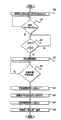
图7A和7B是一个流程图的示例性实施方案,所述流程图概述图4的活动控制电路从“快”频率到“慢”频率的一般频率切换操作。7A and 7B are exemplary embodiments of a flowchart outlining the general frequency switching operation of the active control circuit of FIG. 4 from a "fast" frequency to a "slow" frequency.
图8是一个流程图的示例性实施方案,所述流程图图解图4的活动控制电路的频率切换单元的操作。FIG. 8 is an exemplary embodiment of a flowchart illustrating the operation of the frequency switching unit of the activity control circuit of FIG. 4 .
图9是图形存储控制器中心(GMCH)的第三示例性实施方案,所述图形存储控制器中心与时钟发生器协作来控制显示器使用的频率和/或电压。Figure 9 is a third exemplary embodiment of a graphics memory controller hub (GMCH) that cooperates with a clock generator to control the frequency and/or voltage used by the display.
图10是图9的同步器逻辑的示例性实施方案。FIG. 10 is an exemplary implementation of the synchronizer logic of FIG. 9 .
图11是软件模块的示例性实施方案,所述软件模块控制GMCH的频率和电压节流。Figure 11 is an exemplary implementation of a software module that controls frequency and voltage throttling of the GMCH.
图12是图11软件模块的示例性一般操作图。FIG. 12 is an exemplary general operational diagram of the software module of FIG. 11 .
图13是第一图形用户界面的示例性实施方案,所述第一图形用户界面编程策略以控制计算设备的操作行为。13 is an exemplary embodiment of a first graphical user interface for programming policies to control operational behavior of a computing device.
图14是第二图形用户界面的示例性实施方案,所述第二图形用户界面编程策略以控制计算设备的操作行为。14 is an exemplary embodiment of a second graphical user interface for programming policies to control operational behavior of a computing device.
具体实施方式 Detailed ways
通常,本发明的各种实施方案描述一种装置和方法,用于通过电压和频率调节来控制电子设备的功耗。作为一个实施方案,这个电压和频率控制应用于图形存储控制中心(GMCH)。In general, various embodiments of the present invention describe an apparatus and method for controlling power consumption of electronic devices through voltage and frequency regulation. As an embodiment, this voltage and frequency control is applied to the graphics memory control center (GMCH).
主要按照方块图和流程图呈现下面的详细说明,以便共同图解本发明的各个实施方案。不再详细论述公知的电路或过程操作以避免不必要地混淆对本说明书的理解。The following detailed description is presented primarily in terms of block diagrams and flowcharts for the purpose of collectively illustrating various embodiments of the invention. Well-known circuit or process operations are not discussed in detail to avoid unnecessarily obscuring the understanding of this description.
某个术语被用来描述本发明的某些特征。例如,“计算设备”可以是带有图形存储控制器中心的任何电子产品,例如计算机(如桌上型、膝上型、手提式、服务器、大型机等),或者也许是机顶盒,用户电子设备(如电视机),游戏控制台(game console),或类似物。A certain term is used to describe certain features of the invention. For example, a "computing device" could be any electronic product with a graphics memory controller center, such as a computer (such as a desktop, laptop, hand-held, server, mainframe, etc.), or perhaps a set-top box, a consumer electronic device (such as a television), a game console, or the like.
通常,计算设备包括内部逻辑,即硬件、固件、软件模块或者它们的任何组合。“软件模块”是一系列指令,它们在执行时完成某一功能。软件模块的实施例包括操作系统,应用程序,小应用程序,程序或甚至例程。一个或多个软件模块可以存储在机器可读介质中,所述机器可读介质包括但不局限于电子电路,半导体存储设备,只读存储器(ROM),闪存,可擦写可编程只读存储器类型(EPROM或EEPROM),软盘,致密盘(compact disk),光盘,硬盘,或类似物。术语“逻辑高”和“断言的(asserted)”(或其任何时态)意思是信号进入第一状态,或许在某一电压之上或之下。术语“逻辑低”和“解断言的(deasserted)”(或其任何时态)意思是信号进入不同于第一状态的新状态。Generally, a computing device includes internal logic, ie, hardware, firmware, software modules, or any combination thereof. A "software module" is a series of instructions which, when executed, perform a certain function. Examples of software modules include operating systems, applications, applets, programs, or even routines. One or more software modules may be stored on a machine-readable medium including, but not limited to, electronic circuits, semiconductor memory devices, read-only memory (ROM), flash memory, erasable programmable read-only memory Type (EPROM or EEPROM), floppy disk, compact disk, compact disk, hard disk, or similar. The terms "logic high" and "asserted" (or any tense thereof) mean that a signal enters a first state, perhaps above or below a certain voltage. The terms "logic low" and "deasserted" (or any tense thereof) mean that the signal enters a new state different from the first state.
I、总体结构I. Overall structure
参考图1,图示了在计算设备100内使用的电路的示例性实施方案。计算设备100包括处理器110、时钟发生器120、存储器130和集成设备140(例如图形存储控制器中心(GMCH))。GMCH 140经由总线150和160分别耦合到处理器110和存储器130。如下所述,GMCH 140从时钟发生器120接收参考时钟信号,从电压调节器170接收调节电压(regulated voltages)。尽管未图示,计算设备100可以由一个或多个内置电池供电,或者通过从电源插座经由连接线的交流(AC)电源来进行供电。Referring to FIG. 1 , an exemplary implementation of circuitry for use within a
在这里,处理器110可以是微处理器,数字信号处理器(DSP),专用集成电路(ASIC),微控制器,或类似物。GMCH 140经由总线150(例如前侧总线)耦合到处理器110,以接收要处理并随后要保存在存储器130内或要显示在显示单元180上的信息,所述显示单元与计算设备100相关联。显示单元180可以是计算设备100的整体部件,或者如图所示是与计算设备100分开并在其外部的外围设备。Here, the
时钟发生器120位于计算设备100的内部。然而,设想时钟发生器120可以位于计算设备120的外部。时钟发生器120给处理器110提供第一时钟(HOST_CLK)信号190,并且给GMCH 140提供一个或多个时钟信号。例如,HOST_CLK信号190和次要时钟(CLK2)信号195可以供给GMCH 140,其中CLK2信号195具有比HOST_CLK信号190更低的频率。在一个实施方案中,HOST_CLK信号190和CLK2信号195的频率可以分别是约66兆赫(66MHz)和48兆赫(48MHz)。
II、图形存储控制器中心的实施方案II. Implementation scheme of graphics storage controller center
现在参考图2,图示了图形存储控制器中心(GMCH)140的第一示例性实施方案,所述图形存储控制器中心与时钟发生器120协作来控制核心频率和/或电压的使用。对于本实施方案而言,GMCH 140包括图形核心200、一个或多个时钟源210和215(如锁相环“PLL”电路)、可选分频器电路220、存储控制器225、显示端口230和活动控制电路235。活动控制电路235包括状态定序器240、活动指示器电路245、电压调节控制电路250和核心PLL电路255。Referring now to FIG. 2 , a first exemplary implementation of a graphics memory controller hub (GMCH) 140 that cooperates with
如图2中所示,图形核心200对输入数据执行图形计算,并且经由显示端口230把上述数据输出给图1的显示单元180。图形核心200接收从图1的时钟发生器120产生的参考时钟信号。对于本实施方案而言,GMCH 140接收HOST_CLK信号190,并且把这个时钟信号路由给PLL电路210以及或许路由给分频器电路220。PLL电路210根据HOST_CLK信号190产生存储时钟(MCLK)信号260。与HOST_CLK信号190不同,MCLK信号260是可编程的。MCLK信号260由存储控制器225使用,所述存储控制器控制对图1的存储器130的访问。As shown in FIG. 2 , the
分频器电路220在执行时调节HOST_CLK信号190的频率,并且把调节时钟信号(adjusted clock signal)265传递给核心PLL电路255。核心PLL电路255根据输入的调节时钟信号265产生可编程的绘制(rendering)时钟(CRCLK)信号270,并且为了定时目的,把CRCLK信号270提供给图形核心200。Divider circuit 220 , in execution, adjusts the frequency of
还参考图2,对于本发明的这个实施方案而言,活动控制电路235包括活动指示器电路245,所述活动指示器电路监视GMCH 140的数据处理活动。可以通过检测图形核心200何时是活动的(处理数据)或空闲的来实现上述监视。例如,当图形核心200正在积极处理数据时,由活动指示器电路245检测的控制信号(未图示)被断言(asserted)(例如用于选择极性的逻辑高)。否则,控制信号被解断言(用于选择极性的逻辑低)。通过周期性地采样这个控制信号,可以确定图形核心活动的百分比。根据所述百分比,状态定序器240可以确定CRCLK信号270的频率是否合适或需要改变。Referring also to FIG. 2 , for this embodiment of the invention,
设想除了时钟频率或施加于图形核心200的电压之外,可以配置活动控制电路235来控制计算设备的其他操作行为。实施例包括时钟速度比、时钟调节百分比(clock throttlingpercentages)、刷新率、背后照明光亮度等等。然而,仅仅为了说明的目的,讨论了频率和调节。It is contemplated that
如果核心PLL电路255只支持两个不同时钟频率,则状态定序器240给核心PLL电路255提供断言的控制信号241,以选择较高频率的时钟信号(称为“‘快’频率信号”)。否则,给核心PLL电路255提供解断言的控制信号,以选择较低频率的时钟信号(称为“‘慢’频率信号”)。如果核心PLL电路255支持两个以上不同时钟频率,则状态定序器240可以适合于提供多个控制信号,它们对应于图形核心200的多个时钟频率之一。例如,两个控制信号(00,01,10,11)可以支持四个不同变频时钟。If the
依据对图形核心200的频率改变,状态定序器240还给电压调节器控制电路250提供控制信号242,所述控制电路250给图1的电压调节器(170)发送信号以调节供应给图形核心200的电压。例如,这个电压可以从约1.5V变化到约0.9V或更小。电压调节可以对应于频率变化,并且上述电压调节可以发生在闭锁(ungating)所述的调节时钟信号之前。Depending on the frequency change to the
参考图3,图示了图形存储控制器中心(GMCH)140的第二示例性实施方案,所述图形存储控制器中心与时钟发生器120协作来控制核心频率和/或电压。对于本实施方案而言,GMCH 140排除了调节施加于显示端口230的时钟信号频率的PLL电路215。但GMCH 140以其他部件为特征,例如上面所述的图形核心200,PLL电路210,可选分频器电路220,存储控制器225,显示端口230以及活动控制电路235。Referring to FIG. 3 , a second exemplary implementation of a graphics memory controller hub (GMCH) 140 that cooperates with
III、活动控制电路的实施方案III. Implementation scheme of activity control circuit
A、活动控制电路的示例性逻辑A. Exemplary Logic for Activity Control Circuit
现在参考图4,图示了活动控制电路235的示例性实施方案,尤其是图2和图3的状态定序器240和活动指示器电路245。通常,上述电路包括空闲检测器300、空闲监视器310、减法器350、选择元件(例如多路复用器)360-364、逻辑门370-377以及下面详述的频率切换单元380。通常,频率切换单元380起图2的状态定序器240的作用,而所述电路的其余部分起活动指示器电路245的作用。Referring now to FIG. 4 , an exemplary implementation of the
在本发明的一个实施方案中,为了维持功耗和性能之间的平衡,活动控制电路235支持图1中GMCH 140使用的CRCLK信号270的频率切换。为了消除任何可能的性能损失,空闲监视器310适合于测量图1中GMCH 140的绘制引擎的空闲状态(idleness)。In one embodiment of the invention, in order to maintain a balance between power consumption and performance,
具体地,对于本发明的一个实施方案而言,CRCLK信号270被配置成在达到空闲状态的一个特定阈值(Tf2s)时从“快”频率(Ff)切换到“慢”频率(Fs)(其中Ff>Fs)。称为“快到慢(F2S)状态阈值”的这个阈值可以是静态的,或者可以在上电状态期间通过计算设备的基本输入输出系统(BIOS)或者或许通过访问特定存储位置或寄存器的内容可编程地设定。这个阈值可以表示为如图4所示的位值(例如32位值)。Specifically, for one embodiment of the present invention,
CRCLK信号还被配置成在活动等级增加时从慢频率切换到快频率,从而超过特定活动阈值,称为“慢到快(S2F)状态阈值”(Ts2f)。类似地,可以预置S2F状态阈值,并且用位值表示(例如32位值)。只有CRCLK信号频率可以按照要求动态变化,所有其他时钟将在启动(boot)之后保持不变。The CRCLK signal is also configured to switch from slow to fast frequency as the activity level increases, thereby exceeding a certain activity threshold, referred to as the "slow-to-fast (S2F) state threshold" (T s2f ). Similarly, the S2F state threshold can be preset and represented by a bit value (eg, a 32-bit value). Only the CRCLK signal frequency can be dynamically changed as required, all other clocks will remain unchanged after boot.
除了在测的空闲状态(measured idleness)之外,通过软件控制可以引发其他频率切换事件。例如,可以检测AC电源中断(如通过从电源插座移走它的AC插头面引起连接器线中断),并且使软件例程把CRCLK信号切换到较慢的频率设定,以延长电池寿命。In addition to the measured idleness, other frequency switching events can be triggered through software control. For example, an interruption of AC power (such as a connector wire interruption caused by removing its AC plug face from an electrical outlet) could be detected and a software routine be made to switch the CRCLK signal to a slower frequency setting to preserve battery life.
为了在相同负载下减少不必要的来回切换,可以提供滞后。一种实现此功能的方式是通过确保启动高到低频率转换所需的繁忙等级相当地低于启动低到高频率转换的繁忙等级。频率、系统功率和滞后之间的关系由公式(1)给出:To reduce unnecessary switching back and forth under the same load, hysteresis can be provided. One way to do this is by ensuring that the busy level required to initiate a high-to-low frequency transition is considerably lower than the busy level required to initiate a low-to-high frequency transition. The relationship between frequency, system power and hysteresis is given by equation (1):
(1)Tf2s<Is-((If-Tf2s)*Ff*Is)/(If*Fs)其中(1)T f2s <I s -((I f -T f2s )*F f *I s )/(I f *F s ) where
Tf2s=F2S状态阈值;Ts2f=S2F状态阈值;Is=慢状态间隔;If=快状态间隔;Fs=慢频率;Ff=快频率。T f2s = F2S state threshold; T s2f = S2F state threshold; I s = slow state interval; I f = fast state interval; F s = slow frequency; F f = fast frequency.
下面如图4所示,活动控制电路235的操作部分基于各种控制状态信号。这些控制状态信号包括,但不局限于,GMCH的期望状态(DSTATE)、当前状态(CSTATE)、基于空闲监视器硬件的转变频率请求(HW_CH_FREQ)、和/或基于硬件、软件或热状态的转变频率请求(CH_FREQ_REQ)。As shown below in FIG. 4, the operation of the
更具体地,“DSTATE”表示用于电子设备的期望频率状态等级。DSTATE的值可以保存为空闲状态页(ISP)寄存器390的位(例如ISP[1]),或许位于如图5A所示的GMCH的存储器(未图示)内。ISP寄存器为软件和硬件提供活动和温度信息,以便做出频率和电压调节决策。在这里,对于本发明的这个实施方案而言,断言DSTATE(DSTATE=逻辑“高”)以把CRCLK信号设定和维持在“快”频率水平下。解断言DSTATE(DSTATE=逻辑“低”)以把CRCLK信号设定和维持在“慢”频率水平下。通过硬件或软件可以确定DSTATE。More specifically, "DSTATE" represents a desired frequency state level for an electronic device. The value of DSTATE may be stored as a bit (eg, ISP[1]) of the idle state page (ISP)
当通过硬件确定时,响应图5B中空闲控制和状态(ICS)寄存器395的硬件使能转换位设定(EN_HW_TRAN=ICS[30]=逻辑“高”),与减法器350输出相关联的最高有效位(MSB)等于DSTATE值。否则,当通过软件确定时,DSTATE通常等于软件重置到慢(SWRST2S)信号的反相值(inverted value)(例如ICS[28])。When determined by hardware, the highest value associated with the
在本发明的一个实施方案中,“CSTATE”表示CRCLK信号的当前状态。CSTATE的值可以保存为ISP寄存器390的位(例如ISP[0])。断言CSTATE以把CRCLK信号选择在“快”频率下。解断言CSTATE以选择“慢”频率。所有领域活动停止之后,通过把DSTATE值指定为CSTATE值,将切换CRCLK的频率(例如从快到慢)。In one embodiment of the invention, "CSTATE" represents the current state of the CRCLK signal. The value of CSTATE may be stored as a bit of ISP register 390 (eg, ISP[0]). Assert CSTATE to select the CRCLK signal at a "fast" frequency. Deassert CSTATE to select the "slow" frequency. By specifying the DSTATE value as the CSTATE value, the frequency of the CRCLK will be switched (eg, from fast to slow) after all field activity has ceased.
当断言时,“HW_CH_FREQ”表示硬件确定的转变频率事件(“快”到“慢”或“慢”到“快”)。HW_CH_FREQ是基于空闲监视器的操作。例如,当CRCLK信号在快频率下操作(CSTATE=逻辑“高”)和采样的空闲数量大于F2S状态阈值(Tf2s)时,断言HW_CH_FREQ(HW_CH_FREQ=逻辑“高”)。当CRCLK信号在慢频率下操作(CSTATE=逻辑“低”)和采样的空闲数量小于S2F状态阈值(Ts2f)时,断言HW_CH_FREQ。When asserted, "HW_CH_FREQ" represents a hardware-determined transition frequency event ("fast" to "slow" or "slow" to "fast"). HW_CH_FREQ is an idle monitor based operation. For example, HW_CH_FREQ is asserted (HW_CH_FREQ = logic "high") when the CRCLK signal is operating at a fast frequency (CSTATE = logic "high") and the number of idles sampled is greater than the F2S state threshold (T f2s ). HW_CH_FREQ is asserted when the CRCLK signal is operating at slow frequency (CSTATE = logic "low") and the number of idles sampled is less than the S2F state threshold (T s2f ).
“CH_FREQ_EQ”通常是基于硬件或软件引起的事件和热读数。当断言CH_FREQ_REQ时,它表示针对频率切换单元380的变换频率请求(可以是从快到慢或者从慢到快)。确定CH_FREQ_REQ值以响应两个标准。第一个标准确定是否将提供硬件或软件请求。上述确定是基于EN_HW_TRAN值的(当将提供硬件确定的转变频率请求时,断言EN_HW_TRAN)。"CH_FREQ_EQ" is usually based on hardware or software induced events and thermal readings. When CH_FREQ_REQ is asserted, it represents a request for
第二个标准根据检测到的GMCH温度(TRR[7:0])确定是否需要转变频率请求,GMCH温度可以保存在ISP寄存器390内(例如ISP[9:2])。对于本发明的这个实施方案而言,当检测到的温度在规定阈值之上时,一个THERMALHOT参数设被定为逻辑“1”。然而,即使检测到的温度在规定阈值之上,还允许CRCLK信号从“快”频率发生变化。否则,在断言CSTATE的地方,断言SWITCH_TO_SLOW_IF_HOT(例如IC[29])和THERMALHOT参数,这使得CH_FREQ_REQ被解断言,表示频率水平没有变化。总之,如果检测到的GMCH温度在设定阈值之上,第二个标准用来防止慢到快的频率切换转换。The second criterion determines whether a transition frequency request is required based on the detected GMCH temperature (TRR[7:0]), which can be stored in the ISP register 390 (eg, ISP[9:2]). For this embodiment of the invention, a THERMALHOT parameter is set to logic "1" when the detected temperature is above a specified threshold. However, the CRCLK signal is allowed to change from the "fast" frequency even if the sensed temperature is above the specified threshold. Otherwise, where CSTATE is asserted, SWITCH_TO_SLOW_IF_HOT (eg IC[29]) and THERMALHOT parameters are asserted, which causes CH_FREQ_REQ to be deasserted, indicating no change in frequency level. In summary, the second criterion is used to prevent slow to fast frequency switching transitions if the detected GMCH temperature is above a set threshold.
如图4中所示,当某些单元空闲时,空闲检测器300产生有效整体(Global)空闲(GIDLE)信号309。对于本实施方案而言,这些单元可以包括一个或多个下述单元:MPEG压缩/解压缩单元(MPEG_DONE 302空闲时)、三维绘制单元(3D_DONE 304空闲时)、二维绘制单元或位块传输器(BLT_DONE 306空闲时)和/或硬件组合(hardware binning)单元(HB_DONE 308空闲时)。通过ICS寄存器395内的记录位可以对每个“DONE”信号302,304,306和/或308进行屏蔽(masked)或不进行屏蔽(unmasked),用于测试和提供灵活的活动计数策略。As shown in FIG. 4, the
例如,如图6中所示,ICS寄存器395(ICS[11:8])的四个位400-403唯一地对应于DONE信号302,304,306和308。因此,ICS[11]的设定使第一逻辑门410(例如或门)中的有效信号被输出,以屏蔽MPEG_DONE 302(例如处于断言的逻辑“高”状态)。类似地,ICS[10:8]的设定使从其他逻辑门420,430和440(例如或门)中产生有效信号,以使3D_DONE、BLT_DONE和HB_DONE信号304,306,308也被屏蔽。For example, as shown in FIG. 6 , four bits 400 - 403 of ICS register 395 (ICS[11:8]) uniquely correspond to DONE
返回来参考图4,空闲监视器310适合于在预设时间间隔内确定绘制引擎的空闲率。根据这些空闲测量,空闲监视器310可以产生DSTATE信号和CH_FREQ_REQ信号。软件也可以设定DSTATE信号和CH_FREQ_REQ信号。由于GIDLE 309在每个CRCLK270周期被采样,并且在CRCLK周期内间隔计数器340也正在计数,因此空闲监视器310在CRCLK域中运行。Referring back to FIG. 4 , the
空闲监视器310包括空闲计数器320和间隔计数器340。空闲计数器320包括多个输入321-323。对于本发明的这个实施方案而言,在上电时一旦接收到复位信号(IMrst),清除(CLR)输入321就使空闲计数器320复位。时钟(CLK)输入323允许空闲计数器320通过CRCLK信号270进行计时。一旦接收到断言信号,使能(EN)输入322使空闲计数器320开始计数。如图所示,使能(EN)输入322被耦合到第一逻辑门370(例如与门),当GIDLE信号309被断言并且组合逻辑单元330中的输出被断言时,第一逻辑门370开始计数过程。The
如图所示,组合逻辑单元330包括第二逻辑门371(例如与门功能性),其具有第一输入和第二输入,第一输入从软件接收ICS寄存器(ICS[31])的空闲监视器使能位的值,第二输入耦合到逻辑门372和373(例如与门372和反相器373)的汇集处。组合逻辑单元330输出有效信号以响应(i)间隔计数器340在倒计数顺序期间不越过零(间隔计数器340的最高有效位“IntMSG”被解断言“0”)和(ii)已经断言了开始计数(START_CNT)信号以开始计数顺序。As shown, the
空闲计数器320还包括输出324以把空闲计数传达至ISP寄存器390。对于本实施方案而言,输出是二进制值,其保存在ISP寄存器390的多个位(例如ISP[30:10])内。The
另外,间隔计数器340包括多个输入341-344。对于本实施方案而言,间隔计数器340由CRCLK信号计时,所述CRCLK信号被提供给时钟(CLK)输入端341。负载(LOAD)输入342使间隔计数器340一旦复位就经由数据进入(DIN)输入343加载两个值中的一个。基于CSTATE 347的值,通过选择元件360输出一个值,即快状态间隔(If)345或慢状态间隔(Is)346,CSTATE 347是GMCH的CRCLK信号正在运行的当前状态。使能(EN)输入344一旦接收到断言信号就使间隔计数器340开始计数。如图所示,EN输入344耦合到组合逻辑单元330。Additionally,
一旦间隔计数器340越过零,就断言输出(例如最高有效位的整数值“IntMSB”)348。对于本实施方案而言,这使空闲计数器320和间隔计数器340都停止,因为逻辑门371中的输出被解断言。由空闲计数器320产生的空闲计数然后与CSTATE 347的值一起被采样。空闲计数与S2F状态阈值(Ts2f)351或F2S状态阈值(Tf2s)352进行比较,这些阈值是通过由CSTATE 347控制的选择元件361来输出的。Once the
当采样空闲计数(sampled idle count)超过或者或许等于选择的状态阈值并断言CSTATE 347时,解断言输出信号(MSB)353,并将其路由给逻辑门374(例如异或“XOR(异或)”门)。逻辑门374的输出等于HW_CH_FREQ信号365,即如公式(2)中所示:When the sampled idle count (sampled idle count) exceeds or perhaps equals the selected state threshold and CSTATE 347 is asserted, output signal (MSB) 353 is deasserted and routed to logic gate 374 (e.g. exclusive OR "XOR (exclusive OR) "Door). The output of
(2)
如果由GMCH的硬件确定频率状态,则断言EN_HW_TRAN(ICS[30])以便减法器350中的MSB353从选择元件362输出,并且,因此等于DSTATE_391的值。HW_CH_FREQ信号365经由选择元件363被路由进入选择元件364。If the frequency state is determined by the hardware of the GMCH, EN_HW_TRAN(ICS[30]) is asserted so that
如果检测到的GMCH温度不超出特定阈值,所述GMCH温度作为热值(thermalvalue)保存在ISP寄存器的位中(例如ISP[9:2]),如果CRCLK信号目前运行在“快”频率下,则断言CH_FREQ_REQ信号381并应用于频率切换单元380。可选择地,如果目前运行在“慢”频率下,则解断言CH_FREQ_REQ信号381。If the detected GMCH temperature does not exceed a certain threshold, the GMCH temperature is stored as a thermal value in a bit of the ISP register (eg ISP[9:2]), if the CRCLK signal is currently running at a "fast" frequency, The
如果检测的温度超出特定阈值,则断言THERMALHOT信号并且断言选择元件364的控制信号。因此,如果CRCLK信号的当前频率位于“慢”频率水平(CSTATE=逻辑“低”),则解断言CH_FREQ_REQ信号。然而,如果CRCLK信号的当前频率位于“快”频率水平(CSTATE=逻辑“高”),则断言CH_FREQ_REQ信号381,以允许CRCLK频率降低。If the detected temperature exceeds a certain threshold, the THERMALHOT signal is asserted and the control signal of
如果由软件确定频率状态,则解断言EN_HW_TRAN(例如ICS[30])以便SWRST2S的相反状态设定DSTATE 349的值,该值是由逻辑门375生成的。然后通过由逻辑门376提供的SWRST2S和CSTATE的XOR(异或)结果对频率切换单元380进行有效设定。由逻辑门377提供相同的温度检测替换值(override)。If the frequency state is determined by software, deassert EN_HW_TRAN (eg, ICS[30]) so that the opposite state of SWRST2S sets the value of
B、活动控制电路的示例性操作B. EXEMPLARY OPERATION OF ACTIVITY CONTROL CIRCUIT
现在参考图7A和7B,图示了流程图的示例性实施方案,所述流程图概述图4活动控制电路从“快”到“慢”频率的一般频率切换操作。在这个操作期间,空闲和间隔计数器被初始化(框500),以响应被软件使能。由于断言了CSTATE,第一预置时间间隔在上电时载入间隔计数器(框505)。对于这个具体说明性的实施方案而言,第一预置时间间隔等于快状态间隔。同样,快到慢的阈值载入减法器(框510)。Referring now to FIGS. 7A and 7B , there is illustrated an exemplary embodiment of a flowchart outlining the general frequency switching operation of the active control circuit of FIG. 4 from a "fast" to a "slow" frequency. During this operation, idle and interval counters are initialized (block 500) in response to being enabled by software. Since CSTATE is asserted, the first preset time interval is loaded into the interval counter at power-up (block 505). For this particular illustrative embodiment, the first preset time interval is equal to the fast state interval. Likewise, the fast-to-slow threshold is loaded into the subtractor (block 510).
当断言START_CNT信号时,空闲和间隔计数器将开始计数(框515和520)。当间隔计数器从第一预置时间间隔倒计数时,为CRCLK信号的每一周期断言GIDLE。一旦间隔计数器计数越过零,就断言控制信号,使两个计数器停止(框525和530)。采样空闲计数器的值,CSTATE,DSTATE和确定GMCH当前温度的热值(框535)。When the START_CNT signal is asserted, the idle and interval counters will start counting (blocks 515 and 520). As the interval counter counts down from the first preset time interval, GIDLE is asserted for each cycle of the CRCLK signal. Once the interval counter counts past zero, the control signal is asserted, stopping both counters (blocks 525 and 530). The values of the idle counters, CSTATE, DSTATE, and thermal value are sampled to determine the current temperature of the GMCH (block 535).
如果DSTATE由硬件确定(例如断言EN_HW_TRAN),则在HW_CH_FREQ信号上路由的值等于
如果DSTATE由软件确定(例如解断言EN_HW_TRAN),则如框570中所示,软件转变频率信号(SWCHFREQ)的值等于公式(3):If DSTATE is determined by software (eg, EN_HW_TRAN is deasserted), then as shown in
(3)
因此,如果GMCH的检测温度小于特定阈值,则GMCH的CRCLK信号将经历频率切换操作,该操作对用户是透明的(框555和575)。然而,如果检测温度大于特定阈值,则如果期望转换是到更低的频率,并且断言了SWCHFREQ,则频率切换操作可能还出现(框580)。如果期望转换是到更高的频率,则没有频率切换操作会出现(框565)。Therefore, if the detected temperature of the GMCH is less than a certain threshold, the CRCLK signal of the GMCH will undergo a frequency switching operation, which is transparent to the user (
IV、频率切换单元的示例性操作IV. EXEMPLARY OPERATION OF FREQUENCY SWITCHING UNIT
现在参考图8,图示了图解频率切换单元操作的流程图的示例性实施方案。频率切换单元监视CH_FREQ_REQ信号以及CSTATE和DSTATE的值(框600)。一旦断言了CH_FREQ_REQ信号,并且DSTATE不等于CSTATE,就使能频率切换单元(框605和610)。设想如果断言了CH_FREQ_REQ信号但DSTATE等于CSTATE,则频率切换操作最近已经出现了,从而所述请求被忽视。Referring now to FIG. 8 , an exemplary embodiment of a flowchart illustrating the operation of a frequency switching unit is illustrated. The frequency switching unit monitors the CH_FREQ_REQ signal and the values of CSTATE and DSTATE (block 600). Once the CH_FREQ_REQ signal is asserted and DSTATE is not equal to CSTATE, the frequency switching unit is enabled (
频率切换单元已经被使能之后,假如绘制硬件暂时继续操作直到未决命令的处理已经结束,则某些硬件(例如命令解析器等)操作可以停止以使绘制硬件空闲(框615和620)。此后,选通CRCLK信号(框625)。After the frequency switching unit has been enabled, some hardware (eg, command parser, etc.) operations may be halted to idle the rendering hardware (
已经选通CRCLK信号之后,频率切换单元通过把DSTATE值分配给CSTATE来更新CSTATE值(框630)。此后,闭锁CRCLK信号,并且所述某些硬件和绘制引擎继续操作(框635和640)。这允许频率切换单元在被启动时服务下一个转变频率请求。当然,代替选通CRCLK信号,通过其他方法(例如等待状态)可以实现从一个时钟频率到另一个的平滑转换。如果没有选通CRCLK信号,则在频率切换期间绘制还是可能的,因为不需要等待未决命令结束。After the CRCLK signal has been gated, the frequency switching unit updates the CSTATE value by assigning the DSTATE value to CSTATE (block 630). Thereafter, the CRCLK signal is latched and the certain hardware and rendering engines continue to operate (
参考图9,图示了GMCH的第三示例性实施方案,所述GMCH与时钟发生器协作来控制显示器使用的频率和/或电压。对于本实施方案而言,GMCH 140使用与同步器逻辑710结合起来操作的单个PLL电路700,例如,PLL电路700给图形核心200和存储控制器225提供不同频率的时钟信号。如图所示,同步器逻辑710支持多个时钟频率水平(CLK)。Referring to Figure 9, a third exemplary embodiment of a GMCH that cooperates with a clock generator to control the frequency and/or voltage used by the display is illustrated. For this embodiment,
同步器逻辑710在传输过程中(on the fly)使能频率切换而不需要PLL电路再锁定以及时钟线上的时钟假信号(glitches)。这样的频率切换是出现在从具有快频率(Ff)的时钟信号(CHCLK)到存储时钟频率(MCLK)和从存储时钟频率(MCLK)到具有慢频率(Fs)的时钟信号(CLCLK)。通常,它提供连续的采样方案以允许在交叉定时的逻辑间的确定性的数据传递。
更具体地,如图10中所示,同步器逻辑710的示例性实施方案包括同步器控制逻辑800和同时同步器850。同步器控制逻辑800包括多个采样电路811,812和多个选择元件820(例如多路复用器)。选择元件820交叉连接到采样电路811,812。同步器850包括多个触发器861,862和多个选择元件870-872。More specifically, as shown in FIG. 10 , an exemplary implementation of
每个采样电路采样两个进来的信号的边沿以产生发送(XMIT)信号840和接收(RCV)信号841。这可以通过第一采样电路811采样CHCLK信号830和滞后MCLK信号831的上升沿来实现,以计算XMIT信号840的断言部分。对CHCLK信号830和MCLK信号831的下降沿采样可以被用来计算RCV信号841的解断言部分。类似地,第二采样电路812执行MCLK信号831和滞后CLCLK信号832的边沿采样。Each sampling circuit samples the edges of the two incoming signals to produce a transmit (XMIT) signal 840 and a receive (RCV)
响应解断言的CSTATE值,转换是从慢频率(Fs)到与MCLK相关的中间频率(Fm,这里Fm>Fs)。对于本发明的这个实施方案而言,转换可以通过用CLCLK832来定时图形核心200以及同步器控制逻辑800用同步器850的触发器861和862来控制数据锁存来实现。第一触发器861用CLCLK_832定时,第二触发器862用MCLK_831定时。而且,XMIT信号840和RCV信号841通过选择元件870-871控制数据从图形核心200到存储控制器225的传播。In response to a deasserted CSTATE value, the transition is from the slow frequency (F s ) to the intermediate frequency (F m , where F m >F s ) relative to MCLK. For this embodiment of the invention, switching can be accomplished by clocking
对于从快频率(Ff)到存储控制器频率(Fm,这里Ff>Fm)的转换而言,转换可以通过用CHCLK定时第一触发器861和用MCLK_831定时第二触发器862来实现。此外,XMIT控制信号840和RCV控制信号841通过选择元件870和871控制数据从图形核心200到存储控制器225的传播。旁路信号880控制选择元件872以使数据能绕过第一触发器861。For a transition from fast frequency (F f ) to memory controller frequency (F m , where F f >F m ), the transition can be made by clocking the first flip-
对于GMCH而言,使用多个时钟域。时钟域频率对不同的界面是不同的,其中这些频率间没有好的比率。为了允许在不同频率域运行的逻辑间的确定性传递,已经开发了同步器逻辑710。多路复用器放在触发器前面。同步器控制逻辑将采样时钟边沿,并基于CLCLK和MCLK或CHCLK和MCLK之间的定时边缘(timing margin)(排除设置时间)产生XMIT和RCV信号。同步器810然后将使用这些控制信号。当允许发送时,断言XMIT信号,并且数据穿过多路复用器到达第二触发器。同样的情况应用于接收侧。For GMCH, multiple clock domains are used. Clock domain frequencies are different for different interfaces, where there is no good ratio between these frequencies. To allow deterministic transfer between logic operating in different frequency domains,
现在参考图11,图示了软件模块的示例性实施方案,所述软件模块保存在计算设备的机器可读介质900中,所述软件模块控制GMCH的频率和电压调节。可以配置多个软件模块905以根据多种事件改变频率或电压等级。Referring now to FIG. 11 , an exemplary implementation of software modules stored in a machine-
例如,第一软件模块910可以基于活动(例如绘制引擎的空闲率)增加或降低施加于图形核心的绘制时钟(CRCLK)频率和电压。第二软件模块915可以基于电池功率水平以及计算设备是否连接到AC电源口来改变频率和电压。降低绘制时钟频率来响应减小了的功率水平,所述减小了的功率水平是针对计算设备的一个或多个电池所测得的。第三软件模块920可以基于在围绕所述计算设备的逻辑的外壳内测量的或在计算设备的某些硬件部件上测量的热温度,来改变频率和电压。降低绘制时钟频率来响应这样的热读数(thermal reading),即所述读数超出由用户或制造商设定的预定热限制。For example, the
如图12中所示,图示了软件模块905的示例性总操作,用于通过应用于GMCH的频率和电压调节来进行功率保持。根据选择的功率保持策略950,响应事件955(例如活动/空闲率、功率或热水平等等),可以配置软件905以改变施加于GMCH 140的频率和电压。所述改变是基于“限制”960(例如预选的阈值参数)和“要求”965的。As shown in Figure 12, an exemplary overall operation of the
在这里,对于本发明的某一实施方案而言,存在两种控制计算设备操作行为的一般策略类型:主动的(proactive)和反应的(reactive)。主动的策略针对另一个采取一个策略。例如,如果用户指示一种偏好,即相对性能的最长电池寿命,则软件可以主动地降低功率(例如降低绘制时钟频率),而不需从GMCH接收一个信号。反应策略包括对事件的响应,例如AC连接器的撤除以及平衡用户偏好。Here, for a certain embodiment of the present invention, there are two general types of policies that control the operational behavior of a computing device: proactive and reactive. Active strategies take one strategy against another. For example, if the user indicates a preference for maximum battery life versus performance, software can actively reduce power (eg, reduce draw clock frequency) without receiving a signal from the GMCH. Reaction strategies include responding to events, such as the removal of an AC connector, and balancing user preferences.
如图13和14中所示,用户通过由计算设备生成的图形用户界面1000可以设定这些策略。如图13中所示,用户可以基于计算设备是用电池操作还是接收AC电源来选择不同策略1010。这些策略可以包括例如最大电池寿命1020、最高性能1030或偏向最大电池寿命或最高性能的自适应策略1040。如图14中所示,可以依据“反应”策略条件1060和/或“主动”策略条件1070配置图形用户界面1050。As shown in Figures 13 and 14, a user may set these policies through a
在本发明的一个实施方案中,基于被处理的要求以及要求中的趋势来设计自适应策略,以来进行操作中的转换。基于对事件(例如空闲率、要求、温度)的瞬时测量值以及趋势(例如与事件相关的当前数据样本与一个或多个以前数据样本一起的组合)或历史平均可以计算所述“要求”。另外,自适应策略可以包括进行转换的成本计算(例如每瓦特功率获取的每秒兆位数量)。In one embodiment of the present invention, adaptive strategies are designed to make transitions in operations based on the requirements being processed and trends in the requirements. The "demand" may be calculated based on instantaneous measurements of events (eg, vacancy, demand, temperature) as well as trends (eg, a combination of the current data sample associated with the event along with one or more previous data samples) or historical averages. Additionally, the adaptive strategy may include cost calculations for making the conversion (eg, megabits per second per watt of power harvested).
虽然根据几个说明性实施方案已经对本发明进行了描述,但这中描述不是想要被解释为限制性的。这些说明性实施方案以及本发明其他实施方案的各种修改被视为落入附属权利要求书的精神和范围之内。While this invention has been described in terms of several illustrative embodiments, this description is not intended to be construed in a limiting sense. Various modifications of these illustrative embodiments, as well as other embodiments of the invention, are considered within the spirit and scope of the appended claims.
Claims (19)
Applications Claiming Priority (2)
| Application Number | Priority Date | Filing Date | Title |
|---|---|---|---|
| US10/143,406 | 2002-05-09 | ||
| US10/143,406 US7149909B2 (en) | 2002-05-09 | 2002-05-09 | Power management for an integrated graphics device |
Publications (2)
| Publication Number | Publication Date |
|---|---|
| CN1666166A CN1666166A (en) | 2005-09-07 |
| CN100456209C true CN100456209C (en) | 2009-01-28 |
Family
ID=29400127
Family Applications (1)
| Application Number | Title | Priority Date | Filing Date |
|---|---|---|---|
| CNB03816213XA Expired - Fee Related CN100456209C (en) | 2002-05-09 | 2003-04-02 | Power Management for Integrated Graphics Devices |
Country Status (9)
| Country | Link |
|---|---|
| US (1) | US7149909B2 (en) |
| JP (1) | JP4249701B2 (en) |
| KR (1) | KR100866428B1 (en) |
| CN (1) | CN100456209C (en) |
| AU (1) | AU2003223464A1 (en) |
| DE (1) | DE10392619B4 (en) |
| GB (1) | GB2405009B (en) |
| TW (1) | TWI289806B (en) |
| WO (1) | WO2003096170A2 (en) |
Families Citing this family (83)
| Publication number | Priority date | Publication date | Assignee | Title |
|---|---|---|---|---|
| US7886164B1 (en) | 2002-11-14 | 2011-02-08 | Nvidia Corporation | Processor temperature adjustment system and method |
| US7849332B1 (en) * | 2002-11-14 | 2010-12-07 | Nvidia Corporation | Processor voltage adjustment system and method |
| US7882369B1 (en) | 2002-11-14 | 2011-02-01 | Nvidia Corporation | Processor performance adjustment system and method |
| US7348957B2 (en) * | 2003-02-14 | 2008-03-25 | Intel Corporation | Real-time dynamic design of liquid crystal display (LCD) panel power management through brightness control |
| US6871119B2 (en) * | 2003-04-22 | 2005-03-22 | Intel Corporation | Filter based throttling |
| JP2004355081A (en) * | 2003-05-27 | 2004-12-16 | Internatl Business Mach Corp <Ibm> | Information processing device and memory module |
| US20050057484A1 (en) * | 2003-09-15 | 2005-03-17 | Diefenbaugh Paul S. | Automatic image luminance control with backlight adjustment |
| US20050057485A1 (en) * | 2003-09-15 | 2005-03-17 | Diefenbaugh Paul S. | Image color transformation to compensate for register saturation |
| US7903116B1 (en) * | 2003-10-27 | 2011-03-08 | Nvidia Corporation | Method, apparatus, and system for adaptive performance level management of a graphics system |
| US7155623B2 (en) * | 2003-12-03 | 2006-12-26 | International Business Machines Corporation | Method and system for power management including local bounding of device group power consumption |
| US20050125701A1 (en) * | 2003-12-03 | 2005-06-09 | International Business Machines Corporation | Method and system for energy management via energy-aware process scheduling |
| US7752470B2 (en) * | 2003-12-03 | 2010-07-06 | International Business Machines Corporation | Method and system for power management including device controller-based device use evaluation and power-state control |
| US7356665B2 (en) | 2003-12-17 | 2008-04-08 | International Business Machines Corporation | Method and system for machine memory power and availability management in a processing system supporting multiple virtual machines |
| US7187220B1 (en) * | 2003-12-18 | 2007-03-06 | Nvidia Corporation | Memory clock slowdown |
| US7197652B2 (en) * | 2003-12-22 | 2007-03-27 | International Business Machines Corporation | Method and system for energy management in a simultaneous multi-threaded (SMT) processing system including per-thread device usage monitoring |
| US20050156930A1 (en) * | 2004-01-20 | 2005-07-21 | Matsushita Electric Industrial Co., Ltd. | Rendering device and rendering method |
| US7479753B1 (en) | 2004-02-24 | 2009-01-20 | Nvidia Corporation | Fan speed controller |
| US7698575B2 (en) * | 2004-03-30 | 2010-04-13 | Intel Corporation | Managing power consumption by requesting an adjustment to an operating point of a processor |
| KR20070027598A (en) * | 2004-06-21 | 2007-03-09 | 코닌클리케 필립스 일렉트로닉스 엔.브이. | Power management |
| US8358262B2 (en) | 2004-06-30 | 2013-01-22 | Intel Corporation | Method and apparatus to synchronize backlight intensity changes with image luminance changes |
| US7343502B2 (en) * | 2004-07-26 | 2008-03-11 | Intel Corporation | Method and apparatus for dynamic DLL powerdown and memory self-refresh |
| US7827424B2 (en) * | 2004-07-29 | 2010-11-02 | Ati Technologies Ulc | Dynamic clock control circuit and method |
| US20060095811A1 (en) * | 2004-09-15 | 2006-05-04 | Damon Afualo | Apparatus and method for graphics memory controlling hub (GMCH) clocking support for dual television encoders |
| US7222253B2 (en) * | 2004-12-28 | 2007-05-22 | Intel Corporation | Dynamic power control for reducing voltage level of graphics controller component of memory controller based on its degree of idleness |
| US8593470B2 (en) * | 2005-02-24 | 2013-11-26 | Ati Technologies Ulc | Dynamic memory clock switching circuit and method for adjusting power consumption |
| US7800621B2 (en) * | 2005-05-16 | 2010-09-21 | Ati Technologies Inc. | Apparatus and methods for control of a memory controller |
| US7598959B2 (en) * | 2005-06-29 | 2009-10-06 | Intel Corporation | Display controller |
| US7433191B2 (en) * | 2005-09-30 | 2008-10-07 | Apple Inc. | Thermal contact arrangement |
| JP2007141020A (en) * | 2005-11-21 | 2007-06-07 | Seiko Epson Corp | Data processing apparatus and electronic device |
| US7613941B2 (en) * | 2005-12-29 | 2009-11-03 | Intel Corporation | Mechanism for self refresh during advanced configuration and power interface (ACPI) standard C0 power state |
| US8102398B2 (en) * | 2006-03-03 | 2012-01-24 | Ati Technologies Ulc | Dynamically controlled power reduction method and circuit for a graphics processor |
| US8314806B2 (en) * | 2006-04-13 | 2012-11-20 | Intel Corporation | Low power display mode |
| US7882380B2 (en) * | 2006-04-20 | 2011-02-01 | Nvidia Corporation | Work based clock management for display sub-system |
| US8118483B2 (en) | 2006-06-21 | 2012-02-21 | Intel Corporation | Thermal sensor having toggle control |
| US7882381B2 (en) * | 2006-06-29 | 2011-02-01 | Intel Corporation | Managing wasted active power in processors based on loop iterations and number of instructions executed since last loop |
| US7882384B2 (en) * | 2006-08-31 | 2011-02-01 | National Semiconductor Corporation | Setting and minimizing a derived clock frequency based on an input time interval |
| US7797561B1 (en) | 2006-12-21 | 2010-09-14 | Nvidia Corporation | Automatic functional block level clock-gating |
| US7802118B1 (en) | 2006-12-21 | 2010-09-21 | Nvidia Corporation | Functional block level clock-gating within a graphics processor |
| US7958483B1 (en) * | 2006-12-21 | 2011-06-07 | Nvidia Corporation | Clock throttling based on activity-level signals |
| US9134782B2 (en) | 2007-05-07 | 2015-09-15 | Nvidia Corporation | Maintaining optimum voltage supply to match performance of an integrated circuit |
| US7917789B2 (en) * | 2007-09-28 | 2011-03-29 | Intel Corporation | System and method for selecting optimal processor performance levels by using processor hardware feedback mechanisms |
| US7900497B2 (en) | 2007-12-04 | 2011-03-08 | Hitachi Global Storage Technologies Netherlands B.V. | System, method and apparatus for obtaining true roughness of granular media |
| US7817488B2 (en) * | 2007-12-20 | 2010-10-19 | Sandisk Corporation | Load balancing by using clock gears |
| US8243085B2 (en) * | 2007-12-30 | 2012-08-14 | Intel Corporation | Boosting graphics performance based on executing workload |
| US8370663B2 (en) | 2008-02-11 | 2013-02-05 | Nvidia Corporation | Power management with dynamic frequency adjustments |
| US8525840B2 (en) * | 2008-05-15 | 2013-09-03 | Apple Inc. | Thermal management of graphics processing units |
| US8199158B2 (en) * | 2008-06-11 | 2012-06-12 | Intel Corporation | Performance allocation method and apparatus |
| US9063713B2 (en) * | 2008-10-28 | 2015-06-23 | Apple Inc. | Graphics controllers with increased thermal management granularity |
| KR101047540B1 (en) * | 2009-09-14 | 2011-07-07 | 엠텍비젼 주식회사 | Electronic device and its power consumption control method |
| US8269525B2 (en) * | 2009-11-17 | 2012-09-18 | Ati Technologies Ulc | Logic cell having reduced spurious toggling |
| US9256265B2 (en) | 2009-12-30 | 2016-02-09 | Nvidia Corporation | Method and system for artificially and dynamically limiting the framerate of a graphics processing unit |
| US9830889B2 (en) | 2009-12-31 | 2017-11-28 | Nvidia Corporation | Methods and system for artifically and dynamically limiting the display resolution of an application |
| US8352758B2 (en) * | 2010-03-22 | 2013-01-08 | International Business Machines Corporation | Power bus current bounding using local current-limiting soft-switches and device requirements information |
| US8839006B2 (en) | 2010-05-28 | 2014-09-16 | Nvidia Corporation | Power consumption reduction systems and methods |
| US8533550B2 (en) | 2010-06-29 | 2013-09-10 | Intel Corporation | Method and system to improve the performance and/or reliability of a solid-state drive |
| US8799685B2 (en) | 2010-08-25 | 2014-08-05 | Advanced Micro Devices, Inc. | Circuits and methods for providing adjustable power consumption |
| US8477490B2 (en) | 2011-05-02 | 2013-07-02 | Apple Inc. | Cooling system for mobile electronic devices |
| US9400545B2 (en) | 2011-12-22 | 2016-07-26 | Intel Corporation | Method, apparatus, and system for energy efficiency and energy conservation including autonomous hardware-based deep power down in devices |
| US9105249B2 (en) * | 2011-12-29 | 2015-08-11 | Intel Corporation | Energy conservation in a controller using dynamic frequency selection |
| US9323307B2 (en) * | 2011-12-30 | 2016-04-26 | Intel Corporation | Active display processor sleep state |
| US20140032938A1 (en) * | 2012-07-27 | 2014-01-30 | Texas Instruments Incorporated | Power Management |
| KR101987160B1 (en) | 2012-09-24 | 2019-09-30 | 삼성전자주식회사 | Display driver integrated circuit, display system having the same, and display data processing method thereof |
| US9125299B2 (en) | 2012-12-06 | 2015-09-01 | Apple Inc. | Cooling for electronic components |
| US9275601B2 (en) | 2012-12-12 | 2016-03-01 | Intel Corporation | Techniques to control frame display rate |
| US9098282B2 (en) | 2012-12-27 | 2015-08-04 | Intel Corporation | Methods, systems and apparatus to manage power consumption of a graphics engine |
| US9563253B2 (en) | 2013-03-12 | 2017-02-07 | Intel Corporation | Techniques for power saving on graphics-related workloads |
| US9910473B2 (en) | 2013-03-14 | 2018-03-06 | Silicon Storage Technology, Inc. | Power management for a memory device |
| US9552781B2 (en) | 2013-03-15 | 2017-01-24 | Intel Corporation | Content adaptive LCD backlight control |
| KR101484600B1 (en) | 2013-05-28 | 2015-01-22 | 부산대학교 산학협력단 | Counter-based multi-cycle processor control unit |
| CN103345296B (en) * | 2013-06-04 | 2016-08-10 | 三星半导体(中国)研究开发有限公司 | Dynamic voltage frequency adjustment trigger device and method |
| US9223167B2 (en) | 2013-06-26 | 2015-12-29 | Apple Inc. | Liquid crystal switching barrier thermal control |
| US9389029B2 (en) | 2013-09-30 | 2016-07-12 | Apple Inc. | Heat transfer structure |
| KR102105408B1 (en) | 2013-12-02 | 2020-04-29 | 삼성전자주식회사 | Display driver ic, method thereof, and apparatuses including the same |
| KR102222752B1 (en) | 2014-08-01 | 2021-03-04 | 삼성전자주식회사 | Method of dynamic voltage frequency scaling of processor |
| KR102325453B1 (en) * | 2014-12-04 | 2021-11-11 | 삼성전자주식회사 | Method for operating semiconductor device |
| US9674986B2 (en) | 2015-08-03 | 2017-06-06 | Apple Inc. | Parallel heat spreader |
| US9817431B2 (en) | 2016-02-03 | 2017-11-14 | Qualcomm Incorporated | Frame based clock rate adjustment for processing unit |
| US10754410B2 (en) * | 2018-11-09 | 2020-08-25 | Monolithic Power Systems, Inc. | System and method for standby mode operation of power management system |
| KR20220036232A (en) * | 2020-09-15 | 2022-03-22 | 에스케이하이닉스 주식회사 | Electronic device and method of operation of electronic device |
| US11449125B1 (en) * | 2021-04-01 | 2022-09-20 | Qualcomm Incorporated | Adaptive dynamic clock and voltage scaling |
| US12335422B2 (en) | 2022-01-10 | 2025-06-17 | Apple Inc. | Handheld electronic device |
| CN116449961B (en) * | 2023-06-14 | 2023-10-10 | 蔚来汽车科技(安徽)有限公司 | Input event control methods, systems, electronic devices, storage media and vehicles |
| CN118381583B (en) * | 2024-06-26 | 2024-09-13 | 山东云海国创云计算装备产业创新中心有限公司 | Signal transmission method, apparatus, device, medium and computer program product |
Citations (7)
| Publication number | Priority date | Publication date | Assignee | Title |
|---|---|---|---|---|
| US4841440A (en) * | 1983-04-26 | 1989-06-20 | Nec Corporation | Control processor for controlling a peripheral unit |
| CN1175856A (en) * | 1996-07-05 | 1998-03-11 | 三星电子株式会社 | Video signal conversion device with display mode conversion and display device thereof |
| US5781783A (en) * | 1996-06-28 | 1998-07-14 | Intel Corporation | Method and apparatus for dynamically adjusting the power consumption of a circuit block within an integrated circuit |
| US5987614A (en) * | 1997-06-17 | 1999-11-16 | Vadem | Distributed power management system and method for computer |
| US6018803A (en) * | 1996-12-17 | 2000-01-25 | Intel Corporation | Method and apparatus for detecting bus utilization in a computer system based on a number of bus events per sample period |
| US6125450A (en) * | 1996-12-19 | 2000-09-26 | Intel Corporation | Stop clock throttling in a computer processor through disabling bus masters |
| WO2001073534A2 (en) * | 2000-03-24 | 2001-10-04 | Intel Corporation | Method and apparatus to control processor power and performance for single phase lock loop (pll) processor systems |
Family Cites Families (42)
| Publication number | Priority date | Publication date | Assignee | Title |
|---|---|---|---|---|
| US4238784A (en) * | 1975-01-23 | 1980-12-09 | Colt Industries Operating Corp. | Electronic measuring system with pulsed power supply and stability sensing |
| US4825337A (en) * | 1988-05-17 | 1989-04-25 | Prime Computer, Inc. | Circuit board thermal contact device |
| US5021679A (en) * | 1989-06-30 | 1991-06-04 | Poqet Computer Corporation | Power supply and oscillator for a computer system providing automatic selection of supply voltage and frequency |
| US5153535A (en) * | 1989-06-30 | 1992-10-06 | Poget Computer Corporation | Power supply and oscillator for a computer system providing automatic selection of supply voltage and frequency |
| JP2879694B2 (en) * | 1990-01-29 | 1999-04-05 | 株式会社日立製作所 | Information processing system and external storage device |
| DE69115088T2 (en) * | 1990-03-20 | 1996-05-09 | Fujitsu Ltd | Digital-to-analog converter with a circuit for compensating for output changes that depend on temperature changes. |
| EP0474963A3 (en) | 1990-09-13 | 1992-04-15 | Kabushiki Kaisha Toshiba | Computer system having sleep mode function |
| JPH05119876A (en) | 1991-10-25 | 1993-05-18 | Toshiba Corp | Electronic device and integrated circuit included in the device |
| US5254992A (en) * | 1991-10-31 | 1993-10-19 | Fairbanks Inc. | Low power electronic measuring system |
| US5369771A (en) * | 1991-12-23 | 1994-11-29 | Dell U.S.A., L.P. | Computer with transparent power-saving manipulation of CPU clock |
| JPH05297993A (en) | 1992-04-16 | 1993-11-12 | Dia Semikon Syst Kk | Drive controller for microprocessor |
| US5603036A (en) * | 1993-02-19 | 1997-02-11 | Intel Corporation | Power management system for components used in battery powered applications |
| EP0632360A1 (en) | 1993-06-29 | 1995-01-04 | Xerox Corporation | Reducing computer power consumption by dynamic voltage and frequency variation |
| US5537343A (en) * | 1993-09-02 | 1996-07-16 | Elonex Technologies, Inc. | Digital assistant system having a host computer with a docking bay and a moveable heat sink for cooling a docked module |
| US5721837A (en) * | 1993-10-28 | 1998-02-24 | Elonex I.P. Holdings, Ltd. | Micro-personal digital assistant including a temperature managed CPU |
| US5478221A (en) * | 1994-01-31 | 1995-12-26 | Lzr Electronics, Inc. | Miniature fan for printed circuit board |
| JP2941161B2 (en) * | 1994-02-04 | 1999-08-25 | キヤノン株式会社 | Embedded electronic device and device detaching method in the electronic device |
| US5625829A (en) * | 1994-03-25 | 1997-04-29 | Advanced Micro Devices, Inc. | Dockable computer system capable of symmetric multi-processing operations |
| EP0674275B1 (en) * | 1994-03-25 | 2000-08-09 | Advanced Micro Devices, Inc. | An apparatus and method for achieving hot docking capabilities for a dockable computer system |
| US5598537A (en) * | 1994-03-25 | 1997-01-28 | Advanced Micro Devices, Inc. | Apparatus and method for driving a bus to a docking safe state in a dockable computer system including a docking station and a portable computer |
| US5930110A (en) * | 1994-03-28 | 1999-07-27 | Kabushiki Kaisha Toshiba | Computer system having detachable expansion unit |
| US5664118A (en) * | 1994-03-28 | 1997-09-02 | Kabushiki Kaisha Toshiba | Computer system having detachable expansion unit |
| US5752011A (en) * | 1994-06-20 | 1998-05-12 | Thomas; C. Douglas | Method and system for controlling a processor's clock frequency in accordance with the processor's temperature |
| US5550710A (en) * | 1994-09-09 | 1996-08-27 | Hitachi Computer Products (America), Inc. | Packaging and cooling structure for the personal processor module |
| US5734585A (en) * | 1994-11-07 | 1998-03-31 | Norand Corporation | Method and apparatus for sequencing power delivery in mixed supply computer systems |
| US5745041A (en) * | 1995-07-11 | 1998-04-28 | Dell U.S.A., L.P. | System for dissipating heat from a power supply |
| US5745375A (en) * | 1995-09-29 | 1998-04-28 | Intel Corporation | Apparatus and method for controlling power usage |
| US5798951A (en) * | 1995-12-29 | 1998-08-25 | Intel Corporation | Method and apparatus for automatic un-preconditioned insertion/removal capability between a notebook computer and a docking station |
| US5760636A (en) * | 1996-06-28 | 1998-06-02 | Intel Corporation | Adjusting clock frequency and voltage supplied to a processor in a computer system |
| US6275945B1 (en) * | 1996-11-26 | 2001-08-14 | Kabushiki Kaisha Toshiba | Apparatus for radiating heat for use in computer system |
| US5884049A (en) * | 1996-12-31 | 1999-03-16 | Compaq Computer Corporation | Increased processor performance comparable to a desktop computer from a docked portable computer |
| US5974556A (en) * | 1997-05-02 | 1999-10-26 | Intel Corporation | Circuit and method for controlling power and performance based on operating environment |
| US6052133A (en) * | 1997-06-27 | 2000-04-18 | S3 Incorporated | Multi-function controller and method for a computer graphics display system |
| US6021506A (en) * | 1998-07-31 | 2000-02-01 | Intel Corporation | Method and apparatus for stopping a bus clock while there are no activities on a bus |
| US6460125B2 (en) * | 1998-08-07 | 2002-10-01 | Ati Technologies, Inc. | Dynamic memory clock control system and method |
| US6292201B1 (en) * | 1998-11-25 | 2001-09-18 | Silicon Integrated Systems Corporation | Integrated circuit device having a core controller, a bus bridge, a graphical controller and a unified memory control unit built therein for use in a computer system |
| US6397343B1 (en) * | 1999-03-19 | 2002-05-28 | Microsoft Corporation | Method and system for dynamic clock frequency adjustment for a graphics subsystem in a computer |
| US6848058B1 (en) * | 1999-06-04 | 2005-01-25 | Ati International Srl | Power reduction circuit and method with multi clock branch control |
| US6633987B2 (en) | 2000-03-24 | 2003-10-14 | Intel Corporation | Method and apparatus to implement the ACPI(advanced configuration and power interface) C3 state in a RDRAM based system |
| US6407595B1 (en) * | 2000-04-04 | 2002-06-18 | Silicon Integrated Systems Corp. | Digital clock throttling means |
| US6715089B2 (en) * | 2001-01-22 | 2004-03-30 | Ati International Srl | Reducing power consumption by estimating engine load and reducing engine clock speed |
| US6509788B2 (en) * | 2001-03-16 | 2003-01-21 | Hewlett-Packard Company | System and method utilizing on-chip voltage controlled frequency modulation to manage power consumption |
-
2002
- 2002-05-09 US US10/143,406 patent/US7149909B2/en not_active Expired - Fee Related
-
2003
- 2003-04-02 AU AU2003223464A patent/AU2003223464A1/en not_active Abandoned
- 2003-04-02 WO PCT/US2003/010428 patent/WO2003096170A2/en not_active Ceased
- 2003-04-02 JP JP2004504097A patent/JP4249701B2/en not_active Expired - Fee Related
- 2003-04-02 CN CNB03816213XA patent/CN100456209C/en not_active Expired - Fee Related
- 2003-04-02 DE DE10392619T patent/DE10392619B4/en not_active Expired - Fee Related
- 2003-04-02 GB GB0424629A patent/GB2405009B/en not_active Expired - Fee Related
- 2003-04-02 KR KR1020047017963A patent/KR100866428B1/en not_active Expired - Fee Related
- 2003-04-30 TW TW092110143A patent/TWI289806B/en not_active IP Right Cessation
Patent Citations (7)
| Publication number | Priority date | Publication date | Assignee | Title |
|---|---|---|---|---|
| US4841440A (en) * | 1983-04-26 | 1989-06-20 | Nec Corporation | Control processor for controlling a peripheral unit |
| US5781783A (en) * | 1996-06-28 | 1998-07-14 | Intel Corporation | Method and apparatus for dynamically adjusting the power consumption of a circuit block within an integrated circuit |
| CN1175856A (en) * | 1996-07-05 | 1998-03-11 | 三星电子株式会社 | Video signal conversion device with display mode conversion and display device thereof |
| US6018803A (en) * | 1996-12-17 | 2000-01-25 | Intel Corporation | Method and apparatus for detecting bus utilization in a computer system based on a number of bus events per sample period |
| US6125450A (en) * | 1996-12-19 | 2000-09-26 | Intel Corporation | Stop clock throttling in a computer processor through disabling bus masters |
| US5987614A (en) * | 1997-06-17 | 1999-11-16 | Vadem | Distributed power management system and method for computer |
| WO2001073534A2 (en) * | 2000-03-24 | 2001-10-04 | Intel Corporation | Method and apparatus to control processor power and performance for single phase lock loop (pll) processor systems |
Also Published As
| Publication number | Publication date |
|---|---|
| WO2003096170A3 (en) | 2004-02-05 |
| GB2405009B (en) | 2005-08-24 |
| JP4249701B2 (en) | 2009-04-08 |
| WO2003096170A2 (en) | 2003-11-20 |
| DE10392619T5 (en) | 2005-08-04 |
| TW200404265A (en) | 2004-03-16 |
| GB2405009A (en) | 2005-02-16 |
| JP2005524903A (en) | 2005-08-18 |
| CN1666166A (en) | 2005-09-07 |
| KR20040104713A (en) | 2004-12-10 |
| GB0424629D0 (en) | 2004-12-08 |
| US20030210247A1 (en) | 2003-11-13 |
| US7149909B2 (en) | 2006-12-12 |
| TWI289806B (en) | 2007-11-11 |
| AU2003223464A1 (en) | 2003-11-11 |
| KR100866428B1 (en) | 2008-10-31 |
| DE10392619B4 (en) | 2008-10-16 |
Similar Documents
| Publication | Publication Date | Title |
|---|---|---|
| CN100456209C (en) | Power Management for Integrated Graphics Devices | |
| Rotem et al. | Power management architecture of the 2nd generation intel® core microarchitecture, formerly codenamed sandy bridge | |
| US7529948B2 (en) | Methods and apparatuses for dynamic power estimation | |
| US8578189B2 (en) | Methods and apparatuses for dynamic power control | |
| CN1549961B (en) | Dynamic voltage control method and device | |
| CN1983120B (en) | Data path controller with integrated power management to manage power consumption of a computing device and its components | |
| EP1965287B1 (en) | Microprocessor capable of dynamically increasing its performance in response to varying operating temperature | |
| US7698583B2 (en) | Microprocessor capable of dynamically reducing its power consumption in response to varying operating temperature | |
| CN101025641B (en) | Method and chipset for dynamically increasing data processing rate of computer system during operation | |
| US7100061B2 (en) | Adaptive power control | |
| US9395784B2 (en) | Independently controlling frequency of plurality of power domains in a processor system | |
| CN101454752B (en) | Per die temperature programming for thermally efficient integrated circuit (ic) operation | |
| EP1975761B1 (en) | Microprocessor with improved performance during P-state transitions | |
| GB2539748A (en) | Configuring power management functionality in a processor | |
| US11960340B2 (en) | Performance management during power supply voltage droop | |
| EP4272049A1 (en) | Method and apparatus for providing non-compute unit power control in integrated circuits | |
| EP1965286A2 (en) | Microprocessor with improved thermal monitoring and protection mechanism |
Legal Events
| Date | Code | Title | Description |
|---|---|---|---|
| C06 | Publication | ||
| PB01 | Publication | ||
| C10 | Entry into substantive examination | ||
| SE01 | Entry into force of request for substantive examination | ||
| C14 | Grant of patent or utility model | ||
| GR01 | Patent grant | ||
| CF01 | Termination of patent right due to non-payment of annual fee | ||
| CF01 | Termination of patent right due to non-payment of annual fee |
Granted publication date: 20090128 Termination date: 20180402 |