CN100352036C - Semiconductor device and manufacturing method thereof - Google Patents
Semiconductor device and manufacturing method thereof Download PDFInfo
- Publication number
- CN100352036C CN100352036C CNB200310100556XA CN200310100556A CN100352036C CN 100352036 C CN100352036 C CN 100352036C CN B200310100556X A CNB200310100556X A CN B200310100556XA CN 200310100556 A CN200310100556 A CN 200310100556A CN 100352036 C CN100352036 C CN 100352036C
- Authority
- CN
- China
- Prior art keywords
- film
- mentioned
- dielectric
- wiring
- interlayer dielectric
- Prior art date
- Legal status (The legal status is an assumption and is not a legal conclusion. Google has not performed a legal analysis and makes no representation as to the accuracy of the status listed.)
- Expired - Lifetime
Links
Images


Classifications
-
- H—ELECTRICITY
- H10—SEMICONDUCTOR DEVICES; ELECTRIC SOLID-STATE DEVICES NOT OTHERWISE PROVIDED FOR
- H10W—GENERIC PACKAGES, INTERCONNECTIONS, CONNECTORS OR OTHER CONSTRUCTIONAL DETAILS OF DEVICES COVERED BY CLASS H10
- H10W20/00—Interconnections in chips, wafers or substrates
- H10W20/01—Manufacture or treatment
- H10W20/071—Manufacture or treatment of dielectric parts thereof
- H10W20/074—Manufacture or treatment of dielectric parts thereof of dielectric parts comprising thin functional dielectric layers, e.g. dielectric etch-stop, barrier, capping or liner layers
-
- H—ELECTRICITY
- H10—SEMICONDUCTOR DEVICES; ELECTRIC SOLID-STATE DEVICES NOT OTHERWISE PROVIDED FOR
- H10P—GENERIC PROCESSES OR APPARATUS FOR THE MANUFACTURE OR TREATMENT OF DEVICES COVERED BY CLASS H10
- H10P14/00—Formation of materials, e.g. in the shape of layers or pillars
- H10P14/60—Formation of materials, e.g. in the shape of layers or pillars of insulating materials
- H10P14/66—Formation of materials, e.g. in the shape of layers or pillars of insulating materials characterised by the type of materials
- H10P14/662—Laminate layers, e.g. stacks of alternating high-k metal oxides
-
- H—ELECTRICITY
- H10—SEMICONDUCTOR DEVICES; ELECTRIC SOLID-STATE DEVICES NOT OTHERWISE PROVIDED FOR
- H10P—GENERIC PROCESSES OR APPARATUS FOR THE MANUFACTURE OR TREATMENT OF DEVICES COVERED BY CLASS H10
- H10P14/00—Formation of materials, e.g. in the shape of layers or pillars
- H10P14/60—Formation of materials, e.g. in the shape of layers or pillars of insulating materials
- H10P14/66—Formation of materials, e.g. in the shape of layers or pillars of insulating materials characterised by the type of materials
- H10P14/668—Formation of materials, e.g. in the shape of layers or pillars of insulating materials characterised by the type of materials the materials being characterised by the deposition precursor materials
- H10P14/6681—Formation of materials, e.g. in the shape of layers or pillars of insulating materials characterised by the type of materials the materials being characterised by the deposition precursor materials the precursor containing a compound comprising Si
- H10P14/6682—Formation of materials, e.g. in the shape of layers or pillars of insulating materials characterised by the type of materials the materials being characterised by the deposition precursor materials the precursor containing a compound comprising Si the compound being a silane, e.g. disilane, methylsilane or chlorosilane
-
- H—ELECTRICITY
- H10—SEMICONDUCTOR DEVICES; ELECTRIC SOLID-STATE DEVICES NOT OTHERWISE PROVIDED FOR
- H10P—GENERIC PROCESSES OR APPARATUS FOR THE MANUFACTURE OR TREATMENT OF DEVICES COVERED BY CLASS H10
- H10P14/00—Formation of materials, e.g. in the shape of layers or pillars
- H10P14/60—Formation of materials, e.g. in the shape of layers or pillars of insulating materials
- H10P14/69—Inorganic materials
- H10P14/692—Inorganic materials composed of oxides, glassy oxides or oxide-based glasses
- H10P14/6921—Inorganic materials composed of oxides, glassy oxides or oxide-based glasses containing silicon
- H10P14/6922—Inorganic materials composed of oxides, glassy oxides or oxide-based glasses containing silicon the material containing Si, O and at least one of H, N, C, F or other non-metal elements, e.g. SiOC, SiOC:H or SiONC
- H10P14/6927—Inorganic materials composed of oxides, glassy oxides or oxide-based glasses containing silicon the material containing Si, O and at least one of H, N, C, F or other non-metal elements, e.g. SiOC, SiOC:H or SiONC the material being a silicon oxynitride, e.g. SiON or SiON:H
-
- H—ELECTRICITY
- H10—SEMICONDUCTOR DEVICES; ELECTRIC SOLID-STATE DEVICES NOT OTHERWISE PROVIDED FOR
- H10W—GENERIC PACKAGES, INTERCONNECTIONS, CONNECTORS OR OTHER CONSTRUCTIONAL DETAILS OF DEVICES COVERED BY CLASS H10
- H10W20/00—Interconnections in chips, wafers or substrates
- H10W20/01—Manufacture or treatment
- H10W20/031—Manufacture or treatment of conductive parts of the interconnections
- H10W20/062—Manufacture or treatment of conductive parts of the interconnections by smoothing of conductive parts, e.g. by planarisation
-
- H—ELECTRICITY
- H10—SEMICONDUCTOR DEVICES; ELECTRIC SOLID-STATE DEVICES NOT OTHERWISE PROVIDED FOR
- H10W—GENERIC PACKAGES, INTERCONNECTIONS, CONNECTORS OR OTHER CONSTRUCTIONAL DETAILS OF DEVICES COVERED BY CLASS H10
- H10W20/00—Interconnections in chips, wafers or substrates
- H10W20/01—Manufacture or treatment
- H10W20/071—Manufacture or treatment of dielectric parts thereof
- H10W20/074—Manufacture or treatment of dielectric parts thereof of dielectric parts comprising thin functional dielectric layers, e.g. dielectric etch-stop, barrier, capping or liner layers
- H10W20/075—Manufacture or treatment of dielectric parts thereof of dielectric parts comprising thin functional dielectric layers, e.g. dielectric etch-stop, barrier, capping or liner layers of multilayered thin functional dielectric layers
-
- H—ELECTRICITY
- H10—SEMICONDUCTOR DEVICES; ELECTRIC SOLID-STATE DEVICES NOT OTHERWISE PROVIDED FOR
- H10W—GENERIC PACKAGES, INTERCONNECTIONS, CONNECTORS OR OTHER CONSTRUCTIONAL DETAILS OF DEVICES COVERED BY CLASS H10
- H10W20/00—Interconnections in chips, wafers or substrates
- H10W20/01—Manufacture or treatment
- H10W20/071—Manufacture or treatment of dielectric parts thereof
- H10W20/081—Manufacture or treatment of dielectric parts thereof by forming openings in the dielectric parts
- H10W20/084—Manufacture or treatment of dielectric parts thereof by forming openings in the dielectric parts for dual-damascene structures
- H10W20/086—Manufacture or treatment of dielectric parts thereof by forming openings in the dielectric parts for dual-damascene structures involving buried masks
-
- H—ELECTRICITY
- H10—SEMICONDUCTOR DEVICES; ELECTRIC SOLID-STATE DEVICES NOT OTHERWISE PROVIDED FOR
- H10P—GENERIC PROCESSES OR APPARATUS FOR THE MANUFACTURE OR TREATMENT OF DEVICES COVERED BY CLASS H10
- H10P14/00—Formation of materials, e.g. in the shape of layers or pillars
- H10P14/60—Formation of materials, e.g. in the shape of layers or pillars of insulating materials
- H10P14/63—Formation of materials, e.g. in the shape of layers or pillars of insulating materials characterised by the formation processes
- H10P14/6326—Deposition processes
- H10P14/6328—Deposition from the gas or vapour phase
- H10P14/6334—Deposition from the gas or vapour phase using decomposition or reaction of gaseous or vapour phase compounds, i.e. chemical vapour deposition
- H10P14/6336—Deposition from the gas or vapour phase using decomposition or reaction of gaseous or vapour phase compounds, i.e. chemical vapour deposition in the presence of a plasma [PECVD]
-
- H—ELECTRICITY
- H10—SEMICONDUCTOR DEVICES; ELECTRIC SOLID-STATE DEVICES NOT OTHERWISE PROVIDED FOR
- H10P—GENERIC PROCESSES OR APPARATUS FOR THE MANUFACTURE OR TREATMENT OF DEVICES COVERED BY CLASS H10
- H10P14/00—Formation of materials, e.g. in the shape of layers or pillars
- H10P14/60—Formation of materials, e.g. in the shape of layers or pillars of insulating materials
- H10P14/69—Inorganic materials
- H10P14/6903—Inorganic materials containing silicon
- H10P14/6905—Inorganic materials containing silicon being a silicon carbide or silicon carbonitride and not containing oxygen, e.g. SiC or SiC:H
-
- H—ELECTRICITY
- H10—SEMICONDUCTOR DEVICES; ELECTRIC SOLID-STATE DEVICES NOT OTHERWISE PROVIDED FOR
- H10P—GENERIC PROCESSES OR APPARATUS FOR THE MANUFACTURE OR TREATMENT OF DEVICES COVERED BY CLASS H10
- H10P14/00—Formation of materials, e.g. in the shape of layers or pillars
- H10P14/60—Formation of materials, e.g. in the shape of layers or pillars of insulating materials
- H10P14/69—Inorganic materials
- H10P14/692—Inorganic materials composed of oxides, glassy oxides or oxide-based glasses
- H10P14/6921—Inorganic materials composed of oxides, glassy oxides or oxide-based glasses containing silicon
- H10P14/6922—Inorganic materials composed of oxides, glassy oxides or oxide-based glasses containing silicon the material containing Si, O and at least one of H, N, C, F or other non-metal elements, e.g. SiOC, SiOC:H or SiONC
Landscapes
- Internal Circuitry In Semiconductor Integrated Circuit Devices (AREA)
Abstract
Description
技术领域technical field
本发明涉及半导体器件的制造方法,特别是涉及对于用所谓的金属镶嵌法(Damascene)形成的布线构造和具有这样的布线构造的半导体器件用之有效的技术。The present invention relates to a method of manufacturing a semiconductor device, and particularly relates to a technique effective for a wiring structure formed by a so-called damascene method and a semiconductor device having such a wiring structure.
为了抑制半导体器件的微细化所伴生的布线延迟,就要谋求布线电阻和布线电容的减小。关于布线电阻,人们正在研究用设计技术进行的应对,和采用以铜为主导体层的布线。铜布线的形成,可以采用这样的方法:在包含在绝缘膜上形成的沟的内部的衬底上淀积以铜为主导体层的布线用金属之后,用CMP(化学机械研磨)法除去沟以外的区域的多余的金属,在沟的内部形成布线图形的方法,即所谓的金属镶嵌法。In order to suppress wiring delays associated with miniaturization of semiconductor devices, it is necessary to reduce wiring resistance and wiring capacitance. With regard to wiring resistance, people are studying how to deal with it with design technology, and using wiring with copper as the conductor layer. The formation of copper wiring can adopt such a method: after depositing the metal for wiring with copper as the conductive layer on the substrate including the inside of the groove formed on the insulating film, the groove is removed by CMP (chemical mechanical polishing). The method of forming a wiring pattern inside the groove with excess metal in the area outside the trench is called the damascene method.
另一方面,关于布线电容,人们正在研究采用相对介电常数相对地低到2到3左右的低介电常数材料。其中,那些机械强度优良的含碳的硅氧化物(以下,记为SiOC)膜,作为低介电常数材料被认为是有希望的。On the other hand, with regard to the wiring capacitance, studies are underway to employ low-permittivity materials whose relative permittivity is relatively low to around 2 to 3. Among them, carbon-containing silicon oxide (hereinafter referred to as SiOC) films having excellent mechanical strength are considered to be promising as low dielectric constant materials.
另外,在日本特开2001-326279号公报中,公开了这样的技术:通过使含有具有硅氧烷键的烷基化合物,和调整成气体流量等于或小于该烷基化合物的气体流量的N2O、H2O或CO2之中任何一者的含氧气体的成膜气体等离子体化,使之进行反应,来成膜构成层间绝缘膜的多层的绝缘膜之中那些与铜接连的绝缘膜。In addition, Japanese Patent Application Laid-Open No. 2001-326279 discloses a technique in which an alkyl compound having a siloxane bond is used, and N 2 is adjusted so that the gas flow rate is equal to or less than that of the alkyl compound. O, H 2 O, or CO 2 is a film-forming gas of an oxygen-containing gas that is plasmatized and reacted to form a film that is connected to copper among the multilayer insulating films constituting the interlayer insulating film. insulating film.
此外,在日本特开2001-110789号公报中,记载了淀积和蚀刻由含有硅、氧、和按原子量计算至少约5%的碳的第1电介质层,和含有硅、氧和在第1电介质层内所包含的碳的大约2/3以下的碳的第2电介质层构成的金属间电介质层的方法。In addition, in Japanese Patent Application Laid-Open No. 2001-110789, it is described to deposit and etch a first dielectric layer containing silicon, oxygen, and at least about 5% carbon by atomic weight, and to deposit and etch a first dielectric layer containing silicon, oxygen, and carbon in the first A method of an intermetallic dielectric layer composed of a second dielectric layer that contains about 2/3 or less of the carbon contained in the dielectric layer.
此外,在日本特开2002-203899号公报中,公开了通过用SiO膜、SiOF膜或SiOC膜形成层间绝缘膜,用SiC膜形成阻挡(barrier)膜,来改善层间绝缘膜与阻挡膜之间的粘接性的技术。In addition, in Japanese Patent Application Laid-Open No. 2002-203899, it is disclosed that an interlayer insulating film is formed with a SiO film, a SiOF film, or a SiOC film, and a barrier film is formed with a SiC film to improve the interlayer insulating film and the barrier film. Adhesive technology between.
此外,在日本特开2002-134494号公报中,公开了这样的技术:通过用SiOC膜、SiOF膜或CF膜形成层间绝缘膜,用SiC膜或SiN膜形成CMP时的研磨止挡(stopper)膜和铜阻挡膜,来防止串扰。In addition, Japanese Patent Application Laid-Open No. 2002-134494 discloses a technique in which a polishing stopper (stopper) during CMP is formed with a SiC film or a SiN film by forming an interlayer insulating film with a SiOC film, a SiOF film, or a CF film. ) film and copper barrier film to prevent crosstalk.
此外,在日本特开2002-353310号公报中,公开了通过用SiOC膜形成层间绝缘膜,用SiC膜或SiN膜形成铜阻挡膜,来改善过渡孔的蚀刻的技术。In addition, JP 2002-353310 A discloses a technique for improving the etching of transition holes by forming an interlayer insulating film with a SiOC film and forming a copper barrier film with a SiC film or a SiN film.
此外,在日本特开2003-142593号公报中,公开了通过用SiO膜、SiOF膜或SiOC膜形成层间绝缘膜,用SiC膜或SiN膜形成铜阻挡膜来形成MIM(金属-绝缘体-金属)电容器的技术。In addition, in Japanese Patent Application Laid-Open No. 2003-142593, it is disclosed that an MIM (metal-insulator-metal layer) is formed by forming an interlayer insulating film with a SiO film, a SiOF film, or a SiOC film, and forming a copper barrier film with a SiC film or a SiN film. ) capacitor technology.
此外,在日本特开2003-152076号公报中,公开了通过用SiOC膜、SiOF膜、BN膜或CF膜形成层间绝缘膜,用SiC膜、SiN膜、SiO膜或SiON膜形成CMP时的研磨止挡膜,用SiOC膜或SiON膜形成铜阻挡膜,来改善布线的绝缘击穿耐性的技术。In addition, Japanese Patent Laid-Open No. 2003-152076 discloses that an interlayer insulating film is formed using a SiOC film, a SiOF film, a BN film, or a CF film, and a CMP film is formed using a SiC film, SiN film, SiO film, or SiON film. Technology to improve the insulation breakdown resistance of wiring by polishing the stopper film and forming a copper barrier film with SiOC film or SiON film.
此外,在日本特开2000-200832号公报中,公开了通过用SiO膜、SiOF膜或SiN膜形成层间绝缘膜,用SiC膜或SiN膜形成铜阻挡膜,来改善铜阻挡膜的粘接性的技术。In addition, in Japanese Patent Laid-Open No. 2000-200832, it is disclosed that the adhesion of the copper barrier film is improved by forming an interlayer insulating film with a SiO film, a SiOF film, or a SiN film, and forming a copper barrier film with a SiC film or a SiN film. sex technology.
此外,在日本特开2002-9150号公报中,公开了将铜金属镶嵌布线的铜扩散防止膜做成为由SiN膜、SiC膜或SiCN膜构成的第1绝缘膜,和由SiN膜构成的第2绝缘膜的叠层构造,来防止铜布线的凝集的技术。In addition, Japanese Patent Laid-Open No. 2002-9150 discloses that the copper diffusion prevention film of the copper damascene wiring is made of a first insulating film made of a SiN film, a SiC film, or a SiCN film, and that a first insulating film made of a SiN film is used. 2. A technology to prevent condensation of copper wiring by a laminated structure of insulating films.
此外,在日本特开2002-373936号公报中,公开了作为铜金属镶嵌布线形成时的蚀刻止挡膜,使用SiC膜、SiN膜、SiCN膜或SiON膜的技术。In addition, JP-A-2002-373936 discloses a technique of using a SiC film, SiN film, SiCN film, or SiON film as an etching stopper film when forming copper damascene wiring.
此外,在日本特开2002-170882号公报和特开2002-270691号公报中,公开了在铜金属镶嵌布线的形成中,在实施了向绝缘膜的沟内埋入铜的CMP之后在把铜的表面暴露于氨(NH3)或氦(He)等离子体中进行了表面处理后,形成SiC膜、SiN膜或SiCN膜等的铜扩散防止膜的技术。In addition, JP-A-2002-170882 and JP-A-2002-270691 disclose that, in the formation of copper damascene wiring, after performing CMP for embedding copper into the trenches of the insulating film, the copper A technique in which copper diffusion preventing films such as SiC films, SiN films, or SiCN films are formed after surface treatment by exposure to ammonia (NH 3 ) or helium (He) plasma.
本发明人对金属镶嵌布线的制造方法进行了研究。以下,是本发明人所研究的技术,其概要如下。The inventors of the present invention have studied a method of manufacturing damascene wiring. The following is the technique studied by the present inventors, and its outline is as follows.
首先,向衬底上依次淀积止挡层绝缘膜和布线形成用的绝缘膜(以下,简称为布线层间膜)。布线层间膜可用等离子体CVD法成膜的SiOC膜构成,止挡层绝缘膜,可用例如用等离子体CVD法成膜的硅氧化膜(以下,记为SiO)膜、硅氮化膜(以下,记为SiN)膜或硅碳化氮化膜(以下,记为SiCN)膜构成。止挡层绝缘膜起着蚀刻布线层间膜时的蚀刻止挡层的作用。First, a stopper insulating film and an insulating film for forming wiring (hereinafter, simply referred to as a wiring interlayer film) are sequentially deposited on a substrate. The wiring interlayer film can be composed of a SiOC film formed by plasma CVD, and the stopper insulating film can be, for example, a silicon oxide film (hereinafter referred to as SiO) film or a silicon nitride film (hereinafter referred to as SiO) film formed by plasma CVD. , denoted as SiN) film or silicon carbonitride film (hereinafter denoted as SiCN) film. The stopper insulating film functions as an etching stopper when etching the wiring interlayer film.
其次,用以图形化后的光刻胶膜为掩模的蚀刻技术,在布线层间膜和止挡层绝缘膜的预定的区域上形成布线沟。接着,在包含布线沟的内部的衬底整个面上形成阻挡层例如钛氮化膜,然后形成埋入布线沟的铜膜。铜膜起着主导体层的作用,例如可以用电镀法形成。然后,用CMP除去布线沟以外的区域的铜膜和阻挡层,在布线沟的内部形成铜布线。Next, wiring grooves are formed in predetermined regions of the wiring interlayer film and the stopper insulating film by etching using the patterned photoresist film as a mask. Next, a barrier layer such as a titanium nitride film is formed on the entire surface of the substrate including the interior of the wiring trench, and then a copper film to bury the wiring trench is formed. The copper film functions as a main conductor layer, and can be formed, for example, by electroplating. Then, the copper film and the barrier layer in the region other than the wiring trench were removed by CMP, and copper wiring was formed inside the wiring trench.
其次,为了防止来自铜布线的铜的扩散,在铜布线上形成作为阻挡层起作用的顶包绝缘膜。顶包绝缘膜,可以用例如用CVD法成膜的SiO膜、SiN膜或SiCN构成。该顶包绝缘膜除了作为阻挡层的作用之外,也可以承担作为在铜布线上的绝缘膜形成连接孔时的蚀刻止挡层的作用。Next, in order to prevent diffusion of copper from the copper wiring, a top-clad insulating film functioning as a barrier layer is formed on the copper wiring. The top-clad insulating film can be formed of, for example, a SiO film, SiN film, or SiCN formed by CVD. In addition to the role of the top cladding insulating film as a barrier layer, it can also serve as an etching stopper when forming connection holes in the insulating film on the copper wiring.
但是,伴随着半导体器件的高集成化的要求,对加工尺寸在0.1微米以下的金属镶嵌布线的微细化进行研究时得知:在用CMP研磨铜膜时,在由SiOC膜构成的布线层间膜,和由SiO膜、SiN膜或SiCN膜构成的止挡层绝缘膜之间的界面将产生剥离,存在着使具有金属镶嵌布线的半导体器件的制造成品率降低的问题。However, with the demand for high integration of semiconductor devices, research on the miniaturization of damascene wiring with a processing size of 0.1 micron or less has revealed that when the copper film is polished by CMP, there is a gap between the wiring layers made of the SiOC film. The interface between the SiO film, the SiN film, or the SiCN film and the stopper insulating film delaminates, which has the problem of lowering the manufacturing yield of semiconductor devices having damascene wiring.
发明内容Contents of the invention
本发明的目的在于提供可以提高要形成布线沟的绝缘膜或要形成连接孔的绝缘膜使用SiOC膜的金属镶嵌布线的可靠性的技术。An object of the present invention is to provide a technology capable of improving the reliability of damascene wiring in which an SiOC film is used as an insulating film for forming a wiring trench or an insulating film for forming a contact hole.
本发明的上述以及其它的目的和新的特征,会从本说明书的记述和所附附图中弄明白。The above and other objects and novel features of the present invention will be clarified from the description of this specification and the accompanying drawings.
在本申请中公开的发明之中,简单地说来其代表性的发明如下。Among the inventions disclosed in this application, the representative ones are briefly described as follows.
本发明提供一种在半导体衬底上的层间绝缘膜形成的沟的内部形成金属布线,在上述层间绝缘膜和上述金属布线中的每一者的上部,形成有防止构成上述布线的金属的扩散的顶包绝缘膜的半导体器件,上述层间绝缘膜由SiOC膜,在上述SiOC膜上形成的SiC膜,在上述SiC膜上形成的SiON膜构成,上述顶包绝缘膜由SiCN膜,和在上述SiCN膜上形成的SiC膜构成。The present invention provides a method for forming a metal wiring inside a groove formed by an interlayer insulating film on a semiconductor substrate, and forming a metal wiring on each of the above-mentioned interlayer insulating film and the above-mentioned metal wiring to prevent the formation of the above-mentioned wiring. A semiconductor device with a diffused top-pack insulating film, the above-mentioned interlayer insulating film is composed of a SiOC film, a SiC film formed on the above-mentioned SiOC film, and a SiON film formed on the above-mentioned SiC film, and the above-mentioned top-pack insulating film is composed of a SiCN film, and a SiC film formed on the aforementioned SiCN film.
此外,本发明提供具有金属镶嵌布线的半导体器件的制造方法,用SiOC膜形成要形成布线沟的绝缘膜或要形成连接孔的绝缘膜,与该SiOC膜接连地叠层5nm以上的厚度的SiC膜。In addition, the present invention provides a method of manufacturing a semiconductor device having a damascene wiring, wherein an insulating film for forming a wiring groove or an insulating film for forming a contact hole is formed with a SiOC film, and a SiC film having a thickness of 5 nm or more is laminated successively with the SiOC film. membrane.
本申请中公开的发明之中代表性的发明所得到的效果,简单说来如下。Effects obtained by typical inventions among the inventions disclosed in this application are briefly described as follows.
在要形成布线沟的绝缘膜或要形成连接孔的绝缘膜使用SiOC膜的金属镶嵌布线中,由于用SiC膜,或者用由SiCN膜以及存在于SiOC膜和SiCN膜之间的SiC膜构成的叠层构造构成止挡层绝缘膜或顶包绝缘膜,故可以防止SiOC膜的剥离。由此,能够提高金属镶嵌布线的可靠性。In the damascene wiring using SiOC film as the insulating film for forming the wiring groove or the insulating film for forming the connection hole, since the SiC film is used, or the SiCN film and the SiC film existing between the SiOC film and the SiCN film are used, The laminated structure constitutes a stopper insulating film or a top-pack insulating film, so peeling of the SiOC film can be prevented. Thereby, the reliability of the damascene wiring can be improved.
附图说明Description of drawings
图1是表示作为本发明的实施形式1的CMOSFET的制造方法的半导体衬底的主要部分剖面图。FIG. 1 is a sectional view of a main part of a semiconductor substrate showing a method of manufacturing a CMOSFET according to
图2是表示作为本发明的实施形式1的CMOSFET的制造方法的半导体衬底的主要部分剖面图。2 is a sectional view of a main part of a semiconductor substrate showing a method of manufacturing a CMOSFET according to
图3是表示作为本发明的实施形式1的CMOSFET的制造方法的半导体衬底的主要部分剖面图。3 is a sectional view of a main part of a semiconductor substrate showing a method of manufacturing a CMOSFET according to
图4是表示作为本发明的实施形式1的CMOSFET的制造方法的半导体衬底的主要部分剖面图。4 is a sectional view of a main part of a semiconductor substrate showing a method of manufacturing a CMOSFET according to
图5是表示作为本发明的实施形式1的CMOSFET的制造方法的半导体衬底的主要部分剖面图。5 is a sectional view of a main part of a semiconductor substrate showing a method of manufacturing a CMOSFET according to
图6是表示作为本发明的实施形式1的CMOSFET的制造方法的半导体衬底的主要部分剖面图。6 is a cross-sectional view of a main part of a semiconductor substrate showing a method of manufacturing a CMOSFET according to
图7是表示作为本发明的实施形式1的CMOSFET的制造方法的半导体衬底的主要部分剖面图。7 is a sectional view of a main part of a semiconductor substrate showing a method of manufacturing a CMOSFET according to
图8是表示作为本发明的实施形式2的CMOSFET的制造方法的半导体衬底的主要部分剖面图。8 is a sectional view of a main part of a semiconductor substrate showing a method of manufacturing a CMOSFET according to
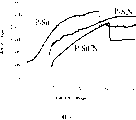
图9是测定绝缘膜(SiC膜、SiCN膜、SiN膜)的TDDB特性的曲线图。FIG. 9 is a graph for measuring TDDB characteristics of an insulating film (SiC film, SiCN film, SiN film).
图10是表示作为本发明的实施形式4的CMOSFET的制造方法的半导体衬底的主要部分剖面图。10 is a sectional view of a main part of a semiconductor substrate showing a method of manufacturing a CMOSFET according to
图11是测定绝缘膜(SiC膜、SiCN膜、SiN膜)的TDDB特性的曲线图。FIG. 11 is a graph for measuring TDDB characteristics of an insulating film (SiC film, SiCN film, SiN film).
图12是对铜布线的应力电徙动特性与SiCN膜和SiC膜的关系进行评价的曲线图。FIG. 12 is a graph evaluating the relationship between stress electromigration characteristics of copper wiring and SiCN film and SiC film.
图13是表示作为本发明的实施形式5的CMOSFET的制造方法的半导体衬底的主要部分剖面图。Fig. 13 is a sectional view of a main part of a semiconductor substrate showing a method of manufacturing a CMOSFET according to
图14是表示作为本发明的实施形式6的CMOSFET的制造方法的半导体衬底的主要部分剖面图。Fig. 14 is a sectional view of a main part of a semiconductor substrate showing a method of manufacturing a CMOSFET according to
图15是表示作为本发明的实施形式7的CMOSFET的制造方法的半导体衬底的主要部分剖面图。15 is a cross-sectional view of a main part of a semiconductor substrate showing a method of manufacturing a CMOSFET according to
具体实施形式Specific implementation form
以下,根据附图详细地说明本发明的实施形式。另外,在用来说明实施形式的所有的图中,作为原则对于相同的构件赋予相同标号而省略其反复的说明。Hereinafter, embodiments of the present invention will be described in detail with reference to the drawings. In addition, in all the drawings for explaining the embodiment, the same reference numerals are assigned to the same components as a principle, and repeated descriptions thereof are omitted.
(实施形式1)(implementation form 1)
用图1到图7示出的半导体衬底的主要部分剖面图按照工序顺序说明作为本发明的实施形式1的CMOSFST(互补金属-氧化物-半导体场效应晶体管)的制造方法。A method of manufacturing a CMOS FST (Complementary Metal-Oxide-Semiconductor Field-Effect Transistor) as
首先,如图1所示,准备例如由P-型的单晶硅构成的半导体衬底1,在半导体衬底1的主面上形成元件隔离区。其次,以图形化后的光刻胶膜为掩模离子注入杂质,形成p阱3和n阱4。向p阱3内离子注入p型杂质,例如离子注入硼,向n阱4内离子注入n型杂质,例如离子注入磷。然后,也可以向各个阱区离子注入用来控制MISFET的阈值的杂质。First, as shown in FIG. 1, a
其次,依次淀积成为栅极绝缘膜5的硅氧化膜,成为栅极电极6的单晶硅膜和成为顶包绝缘膜7的硅氧化膜形成叠层膜,以图形化后的光刻胶膜为掩模对上述叠层膜进行蚀刻。借助于此,形成栅极绝缘膜5、栅极电极6和顶包绝缘膜7。Next, a silicon oxide film to be the
其次,在例如用CVD法向半导体衬底1上淀积了硅氧化膜之后,对该硅氧化膜进行各向异性蚀刻,在栅极电极6的侧壁上形成侧壁衬垫8。然后,以光刻胶膜为掩模,向P阱3内离子注入n型杂质,例如磷或砷,在p阱3的栅极电极6的两侧形成n型半导体区9。n型半导体区9对于栅极电极6和侧壁衬垫8自我匹配地形成,起着n沟MISFET的源漏极的作用。同样,以光刻胶膜为掩模,向n阱4内离子注入p型杂质,例如氟化硼,在n阱4的栅极电极6的两侧形成p型半导体区10。p型半导体区10,对于栅极电极6和侧壁衬垫8自我匹配地形成,起着p沟MISFET的源·漏极的作用。Next, after depositing a silicon oxide film on
其次,如图2所示,用溅射法或CVD法在半导体衬底1上淀积了硅氧化膜之后,用例如CMP法研磨该硅氧化膜,以形成表面平坦化的层间绝缘膜11。接着,用以图形化后的光刻胶膜为掩模的蚀刻,在层间绝缘膜11上形成连接孔12。该连接孔12,在n型半导体区9和p型半导体区10上等的必要部分形成。Next, as shown in FIG. 2, after a silicon oxide film is deposited on the
其次,用例如CVD法在包括连接孔12的内部的半导体衬底1的整个面上形成钛氮化膜,再用例如CVD法形成把连接孔12填埋起来的钨膜。然后,例如用CMP法除去连接孔12以外的区域的钨膜和钛氮化膜,在连接孔12内部形成针形接点13。Next, a titanium nitride film is formed on the entire surface of the
接着,用单金属镶嵌法形成第1布线层。首先,在针形接点13上形成止挡层绝缘膜14,再形成布线层间膜15。由于要在止挡层绝缘膜14和布线层间膜15形成下面要说明的第1布线层,故其合计膜厚可由对第1布线层所必要的设计膜厚决定。Next, the first wiring layer is formed by the single damascene method. First, a
止挡层绝缘膜14,是在对布线层间膜15进行布线沟加工时成为蚀刻止挡层的膜,可用对布线层间膜15具有蚀刻选择比的材料构成。止挡层绝缘膜14,作为氮的含量在1%以下的硅碳化(以下,记为SiC)膜,其膜厚可以做成为例如约5nm以上。SiC膜可以用例如等离子体CVD法形成,其成膜条件例如为:rf功率200~1000W、压力2~10Torr、温度300~400℃、气体为含C气体(例如烷基硅烷)和He,气体流量为100~2000sccm。布线层间膜15由SiOC膜构成,相对介电常数约为3左右。SiOC膜可用例如CVD法形成,其成膜条件例如为:rf功率200~1000W、压力2~10Torr、温度300~400℃、气体为含C气体(例如烷基硅烷)和He和氧气,气体流量为100~2000sccm。The
另外,构成止挡层绝缘膜14的SiC膜和构成布线层间膜15的SiOC膜,可用一台等离子体CVD装置形成。可以举出例如用在等离子体CVD装置中具备的2个反应室,在各自的反应室中成膜SiC膜和SiOC膜的方法,或用一个反应室通过改变气体等成膜条件连续成膜SiC膜和SiOC膜的方法的例子。Further, the SiC film constituting the
接着,用以图形化后的光刻胶膜为掩模的蚀刻,在止挡层绝缘膜14和布线层间膜15的预定的区域上形成布线沟16。Next,
其次,在包括布线沟16的内部的半导体衬底1的整个面上形成阻挡金属层17。阻挡金属层17,由例如钽膜构成,其厚度,例如可以做成为在衬底平面上约50nm左右。上述钽膜,可以用例如溅射法形成。阻挡金属层17,也可以用钛氮化膜、钽氮化膜等构成。Next,
接着,在阻挡金属层17上,用例如CVD法或溅射法形成铜的籽晶层(未画出来),再用例如电解电镀法在籽晶层上形成铜膜18。Next, a copper seed layer (not shown) is formed on the
其次,如图3所示,用CMP法研磨除去铜膜18和籽晶层,再继续研磨,除去布线层间膜15上的阻挡金属层17。借助于此,除去布线沟16以外的区域的铜膜18(包括籽晶层)和阻挡金属层17,形成第1布线层的布线19。Next, as shown in FIG. 3 , the
然而,在用SiO膜、SiN膜或SiCN膜构成止挡层绝缘膜,用SiOC膜构成布线层间膜的本发明人所研究的技术的情况下,在铜膜和阻挡金属层的CMP工序中止挡层绝缘膜和布线层间膜之间的界面产生了剥离。但是,在用SiC膜构成止挡层绝缘膜14,用Si0C膜构成布线层间膜15的本实施形式1的情况下,在止挡层绝缘膜(SiC膜)和布线层间膜(SiOC膜)之间的界面未产生剥离。However, in the case of the technology studied by the present inventors in which the stopper insulating film is formed of an SiO film, SiN film, or SiCN film, and the wiring interlayer film is formed of an SiOC film, the CMP process of the copper film and the barrier metal layer is suspended. The interface between the barrier insulating film and the wiring interlayer film was delaminated. However, in the case of
表1Table 1

在表1中,归纳示出了各种绝缘膜的杨氏模量、应力和含氮量。SiOC膜和各种绝缘膜的粘接性按照SiN膜、SiCN膜、SiO膜、SiC膜的顺序变小,这表明具有依赖于含氮量的倾向。此外,杨氏模量按照SiN膜、SiCN膜、SiO膜、SiC膜的顺序变小。此外,SiOC膜和SiC膜呈现出拉伸应力,而SiN膜、SiCN膜、Si0膜呈现出压缩应力。In Table 1, Young's modulus, stress, and nitrogen content of various insulating films are summarized. The adhesion between the SiOC film and various insulating films decreases in the order of the SiN film, the SiCN film, the SiO film, and the SiC film, showing a tendency to depend on the nitrogen content. In addition, the Young's modulus becomes smaller in the order of the SiN film, the SiCN film, the SiO film, and the SiC film. In addition, SiOC films and SiC films exhibit tensile stress, while SiN films, SiCN films, and SiO films exhibit compressive stress.
由这些情况可知,在SiOC膜的界面,可以认为用O、C封端的分子构造因加强了在界面处的原子间的结合而改善了粘接性。此外,还可以认为是由于与SiOC膜接连起来地设置与SiOC膜具有相同拉伸应力、与SiOC膜之间的杨氏模量之差为50GPa以下、应力差为50GPa以下的SiC膜,缓和了SiC膜在铜膜的CMP处理时产生的纵横方向的加载,抑制了SiOC膜与SiC膜之间的界面上的剥离。From these facts, at the interface of the SiOC film, it is considered that the molecular structure terminated with O and C improves the adhesion by strengthening the bond between atoms at the interface. In addition, it can also be considered that since the SiC film having the same tensile stress as the SiOC film, the difference in Young's modulus with the SiOC film is 50 GPa or less, and the stress difference is 50 GPa or less, the SiC film is placed next to the SiOC film. The loading of the SiC film in the vertical and horizontal directions generated during the CMP treatment of the copper film suppresses peeling at the interface between the SiOC film and the SiC film.
另外,在这里,作为止挡层绝缘膜14虽然举出的是SiC膜,但是,也可以用与SiOC膜之间的杨氏模量之差在50GPa以下或应力差为50GPa以下的绝缘膜构成止挡层绝缘膜14。此外,虽然是用等离子体CVD法形成构成止挡层绝缘膜14的SiC膜,并例示出了其成膜条件,但是制造方法或成膜条件,并不限定于此。In addition, here, although the SiC film is cited as the stopper
其次,用双金属镶嵌法形成第2布线层。首先,如图4所示,在第1布线层19上依次形成顶包绝缘膜20、要形成连接孔的绝缘膜(以下,简称为孔层间膜)21和布线形成用的止挡层绝缘膜22。Next, the second wiring layer is formed by the dual damascene method. First, as shown in FIG. 4 , on the
顶包绝缘膜20,可以是含氮量为1%以下的SiC膜,其厚度,例如可以是约5nm以上。此外,顶包绝缘膜20虽然具有防止铜的扩散的功能,但是也可以用对孔层间膜21具有蚀刻选择比的材料构成,可以用作对孔层间膜21进行连接孔加工时的蚀刻止挡层。SiC膜可以用例如CVD法形成,其成膜条件例如可以使用与构成上述止挡层绝缘膜14的SiC膜大体上同样的条件。The top clad insulating
孔层间膜21,由SiOC膜构成,SiOC膜例如可以用等离子体CVD法形成,其成膜条件例如可以使用与构成上述布线层间膜15的SiOC膜大体上同样的条件。
止挡层绝缘膜22,可以用对在孔层间膜21和之后在止挡层绝缘膜22的上层淀积的布线层间膜具有蚀刻选择比的绝缘材料构成,作成为含氮量在1%以下的SiC膜,其膜厚可以是例如约5nm以上。SiC膜例如可以用CVD法形成,其成膜条件例如可以使用与构成上述止挡层绝缘膜14的SiC膜大体上同样的条件。The
其次,止挡层绝缘膜22上形成已图形化为孔图形的光刻胶膜,以该光刻胶膜为掩模蚀刻止挡层绝缘膜22。Next, a photoresist film patterned into a hole pattern is formed on the
接着,在止挡层绝缘膜22上形成布线层间膜23。布线层间膜23由SiOC膜构成,SiOC膜可以用例如CVD法形成,其成膜条件例如可以使用与构成上述布线层间膜15的SiOC膜大体上同样的条件。另外,由于在止挡层绝缘膜22和布线层间膜23要形成埋入其次要说明的第2布线层的布线沟,故其合计膜厚可以由对第1布线层所必要的设计膜厚决定。Next, a
然后,如图5所示,在布线层间膜23上形成已图形化为沟图形的光刻胶膜,以该光刻胶膜为掩模蚀刻布线层间膜23。这时,顶包绝缘膜22将起着蚀刻止挡层的作用。Then, as shown in FIG. 5, a photoresist film patterned into a groove pattern is formed on the
接着,以上述光刻胶膜和止挡层绝缘膜22为掩模,蚀刻孔层间膜21。这时顶包绝缘膜20将起着蚀刻止挡层的作用。Next, the
接着,例如用干式蚀刻法除去已露出来的顶包绝缘膜20。在除去顶包绝缘膜20的同时除去止挡层绝缘膜22,在顶包绝缘膜20和孔层间膜21形成连接孔24,在止挡层绝缘膜22和布线层间膜23形成布线沟25。Next, the exposed top-
其次,如图6所示,在包括连接孔24和布线沟25的内部的半导体衬底1的整个面上形成阻挡金属层26。阻挡金属层26,例如由钽膜构成,其厚度可以是例如在衬底平面上约50nm左右。上述钽膜,例如可以用溅射法形成。阻挡金属层26,也可以用钛氮化膜、钽氮化膜等构成。Next, as shown in FIG. 6 , a
接着,在阻挡金属层26上,例如用CVD法或溅射法形成铜的籽晶层(未画出来),再用例如电解电镀法在籽晶层上形成铜膜27。Next, a copper seed layer (not shown) is formed on the
其次,如图7所示,用CMP法研磨除去铜膜27和籽晶层,再继续研磨,除去布线层间膜23上的阻挡金属层26。借助于此,除去布线沟26以外的区域的铜膜27(包括籽晶层)和阻挡金属层26,形成与连接构件形成为一体的第2布线层的布线28。Next, as shown in FIG. 7, the
在该铜膜27(包括籽晶层)和阻挡金属层26的CMP工序中,也与上所说的铜膜18(包括籽晶层)和阻挡金属层17的CMP工序的情况同样,在顶包绝缘膜(SiC膜)20和孔层间膜(SiOC膜)21之间的界面,在孔层间膜(SiOC膜)21和止挡层绝缘膜(SiC膜)22之间的界面,止挡层绝缘膜(SiC膜)22和布线层间膜(SiOC膜)23之间的界面,未发生剥离。In the CMP process of the copper film 27 (including the seed layer) and the
接着,虽然未画出来,先在第2布线层的布线28上形成顶包绝缘膜29,再在形成了其上层的布线之后,用钝化膜把半导体衬底1覆盖起来,就大体上完成了CMOFET。Next, although it is not shown, the top-coat insulating film 29 is first formed on the
另外,在本实施形式1中,在用双金属镶嵌法形成第2布线层的布线28的情况下,虽然在止挡层绝缘膜22上预先加工孔图形之后,使顶包绝缘膜20和止挡层绝缘膜22作为蚀刻止挡层发挥作用,同时在孔层间膜21上形成连接孔24,在布线层间膜23形成布线沟25,但是,并不限定于此。还有如下的方法:例如,在用以图形化为孔图形的光刻胶膜为掩模的蚀刻,在布线层间膜23和孔层间膜21形成了连接孔23后,用以已图形化为沟图形的光刻胶膜为掩模的蚀刻,在布线层间膜23形成布线沟的方法,或在用以已图形化为孔图形的光刻胶膜为掩模的蚀刻,在布线层间膜23形成了布线沟24之后,用以已图形化为孔图形的光刻胶膜为掩模的蚀刻,在孔层间膜21形成连接孔23的方法,等等。In addition, in the first embodiment, in the case of forming the
如上所述,倘采用本实施形式,在用作为相对地低的低介电常数材料的SiOC膜构成布线层间膜15、23和孔层间膜21的情况下,由于用SiC膜构成与线层间膜15、23和孔层间膜21接连地设置的止挡层绝缘膜14、22和顶包绝缘膜20,故可以防止形成第1布线层19的CMP工序的布线层间膜15和止挡层绝缘膜14之间的界面处的剥离,和形成第2布线层的布线20的CMP工序的顶包绝缘膜20与孔层间膜21之间的界面、孔层间膜21与止挡层绝缘膜22之间的界面、止挡层绝缘膜22与布线层间膜23之间的界面处的剥离。As described above, according to this embodiment, in the case where the
(实施形式2)(implementation form 2)
用图8所示的半导体衬底的主要部分剖面图说明作为本发明的实施形式2的CMOSFET的制造方法。A method of manufacturing a CMOSFET according to
在上述实施形式1中,用SiC膜构成止挡层绝缘膜14、22和顶包绝缘膜20,在本实施形式2中,则用与SiC膜比较可以把漏电流抑制得小的SiCN膜A,以及存在于构成布线层间膜15、23和孔层间膜21的SiOC膜与上述SiCN膜A之间的SiC膜B构成。SiCN膜A的厚度,例如为40nm左右,SiC膜B的厚度,例如为10nm左右,SiCN膜A的含氮量为至少1%。In the above first embodiment, the stopper
此外,SiCN膜A,例如可以用等离子体CVD法形成,其成膜条件例如为:rf功率200~1000W、压力2~10Torr、温度300~400℃、气体为含C气体(例如烷基硅烷)和NH3和He,气体流量为100~2000sccm。SiC膜B,例如可以用等离子体CVD法形成,其成膜条件例如为:rf功率200~1000W、压力2~10Torr、温度300~400℃、气体为含C气体(例如烷基硅烷)和He,气体流量为100~2000sccm。In addition, the SiCN film A can be formed by, for example, plasma CVD, and its film forming conditions are, for example: rf power 200-1000W, pressure 2-10Torr, temperature 300-400°C, gas containing C (for example, alkyl silane) And NH 3 and He, the gas flow rate is 100-2000 sccm. SiC film B, for example, can be formed by plasma CVD, and its film forming conditions are, for example: rf power 200-1000W, pressure 2-10Torr, temperature 300-400°C, gas containing C gas (such as alkyl silane) and He , The gas flow rate is 100-2000 sccm.
图9是测定3种绝缘膜(SiC膜、SiCN膜、SiN膜)的漏电流特性的曲线图,横轴是电场强度(单位:MV/cm),纵轴是膜的漏电流(单位:A/cm2)。由曲线图可知,在电场强度=3MV/cm处的漏电流,SiCN膜最小,SiC膜最大。Fig. 9 is a graph measuring the leakage current characteristics of three insulating films (SiC film, SiCN film, SiN film), the horizontal axis is the electric field intensity (unit: MV/cm), and the vertical axis is the leakage current of the film (unit: A /cm 2 ). It can be seen from the graph that the leakage current at the electric field strength = 3MV/cm is the smallest for the SiCN film and the largest for the SiC film.
如上所述,倘采用本实施形式2,由于主要用漏电流相对地小的SiCN膜A构成止挡层绝缘膜14、22和顶包绝缘膜20,且在构成布线层间膜15、23和孔层间膜21的SiOC膜与上述SiCN膜之间存在有SiC膜B,故在可以减小布线间的漏电流的同时,还可以防止SiOC膜的剥离。As described above, according to
(实施形式3)(implementation form 3)
在本实施形式中,用含氮的SiOC膜构成布线层间膜15、22和孔层间膜21,用漏电流相对地小的SiCN膜构成止挡层绝缘膜14、22和顶包绝缘膜20。含氮的SiOC膜,例如可以用等离子体CVD法形成,其成膜条件例如为:rf功率200~1000W、压力2~10Torr、温度300~400℃、气体为含C气体(例如烷基硅烷)和O2和N2,或者,含C气体(例如烷基硅烷)和N2O、气体流量为100~2000sccm。SiCN膜,例如可以用等离子体CVD法形成,其成膜条件例如为:rf功率200~1000W、压力2~10Torr、温度300~400℃、气体为含C气体(例如烷基硅烷)NN3和He,气体流量为100~2000sccm。SiCN膜的厚度例如为50nm左右。In this embodiment, the
如上所述,倘采用本实施形式3,由于在SiOC膜内含有氮,故可以提高两者的粘接性。借助于此,就可以在减小布线间的漏电流的同时,防止SiOC膜的剥离。As described above, according to the third embodiment, since nitrogen is contained in the SiOC film, the adhesion between the two can be improved. With this, it is possible to prevent the peeling of the SiOC film while reducing the leakage current between wirings.
(实施形式4)(implementation form 4)
如图10所示,在本实施形式4中,用SiCN膜A和SiC膜B的叠层膜构成止挡层绝缘膜14、22和顶包绝缘膜20中的每一者。As shown in FIG. 10, in
图11是测定3种绝缘膜(SiC膜、SiCN膜、SiN膜)的TDDB(Time-dependent dielectric breakdown,时间经过性绝缘击穿)特性的曲线图。横轴为电场强度(单位:MV/cm),纵轴表示TDDB寿命(单位:秒)。从该图显而易见,与SiC膜相比SiCN膜的TDDB寿命长。FIG. 11 is a graph showing TDDB (Time-dependent dielectric breakdown) characteristics of three types of insulating films (SiC film, SiCN film, and SiN film). The horizontal axis represents electric field intensity (unit: MV/cm), and the vertical axis represents TDDB lifetime (unit: second). As apparent from this figure, the TDDB life of the SiCN film is longer than that of the SiC film.
另一方面,图12是评价铜布线(过渡孔部分)的应力电徙动特性和SiCN膜以及SiC膜的关系的曲线图,横轴为铜布线的线条宽度(单位:微米),纵轴是由应力电徙动产生的布线的不良率(单位:%)。由曲线图可知,当铜布线的线条宽度成为某一值以上时,SiCN膜铜布线的应力电徙动特性显著地劣化,而SiC膜与铜布线的线条宽度无关,应力电徙动特性几乎没有变化。此外,SiCN膜和SiC膜的叠层膜则显示出它们的之间的特性。On the other hand, FIG. 12 is a graph for evaluating the relationship between the stress electromigration characteristics of the copper wiring (transition hole portion) and the SiCN film and the SiC film. The horizontal axis is the line width of the copper wiring (unit: micron), and the vertical axis is Defect rate (unit: %) of wiring due to stress electromigration. It can be seen from the graph that when the line width of the copper wiring exceeds a certain value, the stress electromigration characteristics of the SiCN film copper wiring deteriorate significantly, while the SiC film has almost no stress electromigration characteristics regardless of the line width of the copper wiring. Variety. In addition, the laminated film of the SiCN film and the SiC film shows characteristics between them.
由以上可知,由于用SiCN膜A和SiC膜B的叠层膜构成止挡层绝缘膜14、22和顶包绝缘膜20中的每一者,故在可以防止止挡层绝缘膜14、22和顶包绝缘膜20的TDDB特性的劣化的同时,还可以实现漏电流的减少,而可以防止铜布线的应力电徙动特性的劣化。From the above, since each of the
另外,在用SiCN膜A和SiC膜B的叠层膜构成止挡层绝缘膜14、22和顶包绝缘膜20中的每一者的情况下,构成布线层间膜15、22和孔层间膜21的SiOC膜与SiCN膜A之间的界面的粘接力将会降低。于是,在本实施形式中,用SiOC膜C、SiC膜B和SiON膜D这3层构造构成布线层间膜15、22和孔层间膜21中的每一者,使得SiOC膜和SiCN膜A不直接接触。在这里在SiOC膜C和SiON膜D之间的薄的SiC膜B,是用来提高SiOC膜C和SiCN膜A之间的粘接性的粘接层。此外,为了尽可能地降低布线层间膜15、23和孔层间膜21的介电常数,介电常数比SiOC膜高的SiON膜D的膜厚,理想的是比SiOC膜C更薄,并且使含氮量成为5atom%以下。SiON膜D,例如可以用把单硅烷(SiH4)和一氧化二氮(N2O)用做源气体的等离子体CVD法(成膜温度=350~400℃)进行淀积。In addition, in the case where each of the
(实施形式5)(implementation form 5)
在像实施形式4那样,用SiOC膜C、SiC膜B和SiON膜D这3层构造构成布线层间膜15、23和孔层间膜21中的每一者的情况下,由于作为粘接层的SiC膜B的蚀刻选择比与SiOC膜C和SiON膜D的蚀刻选择比不同,故存在着在用来形成布线沟16、25或连接孔24的蚀刻工序中SiC膜B成为蚀刻止挡膜,使吞吐率降低的问题。In the case of constituting each of the
于是,在本实施形式中,如图13所示,用SiOC膜C和SiON膜D这2层构造构成布线层间膜15、23和孔层间膜21中的每一者,防止在形成布线沟16、25或连接孔24时蚀刻的吞吐率的降低。Therefore, in this embodiment, as shown in FIG. 13, each of the
另一方面,在省略作为粘接层的SiC膜B的情况下,则存在着在SiOC膜C和SiON膜D的界面的粘接力降低,易于产生膜的剥离这样的问题。On the other hand, when the SiC film B as the adhesive layer is omitted, the adhesive force at the interface between the SiOC film C and the SiON film D decreases, and there is a problem that peeling of the film tends to occur.
作为膜的剥离的原因之一,人们认为在于:相对于SiOC膜C的成膜后的室温下的应力为45MPa(拉伸应力),在450℃下的应力成为-16MPa(压缩应力),膜应力变化从拉伸应力变成为压缩应力,此外,其变化量大到61MPa(45MPa-(-16MPa))。As one of the reasons for the peeling of the film, it is considered that the stress at room temperature after SiOC film C is 45 MPa (tensile stress) after film formation, and the stress at 450° C. is -16 MPa (compressive stress). Stress changes from tensile stress to compressive stress, and the change is as large as 61MPa (45MPa-(-16MPa)).
作为其对策,可以考虑采用在高温(例如成膜温度=375℃)下淀积SiOC膜C的办法,使在SiOC膜C的成膜后的室温下的应力,从53MPa(拉伸应力)变成为在450℃下的78MPa(拉伸应力),其变化量为25Mpa(78Mpa-53Mpa),变成为由温度变化所产生的应力变动量小的膜,使得SiON膜之间的粘接性提高。此外,如果在使SiOC膜C成膜后,对其表面进行氦(He)等离子体处理或氧等离子体处理,接着,淀积SiON膜D,则可以提高两者的粘接力。另外,当SiOC膜C的淀积温度过高或等离子体处理过度,则SiOC膜C的介电常数会降低,故成膜温度以在300℃以下,等离子体处理时间在20秒以下(例如15秒左右)为好。As a countermeasure, it is conceivable to adopt a method of depositing SiOC film C at a high temperature (for example, film formation temperature = 375° C.), so that the stress at room temperature after SiOC film C is formed can be changed from 53 MPa (tensile stress) to It becomes 78MPa (tensile stress) at 450°C, and its variation is 25Mpa (78Mpa-53Mpa). It becomes a film with a small stress variation caused by temperature change, making the adhesion between SiON films improve. Furthermore, if the SiOC film C is formed, the surface thereof is subjected to helium (He) plasma treatment or oxygen plasma treatment, and then the SiON film D is deposited, the adhesion between the two can be improved. In addition, when the deposition temperature of the SiOC film C is too high or the plasma treatment is excessive, the dielectric constant of the SiOC film C will decrease, so the film formation temperature should be below 300°C, and the plasma treatment time should be below 20 seconds (for example, 15 seconds). seconds or so) is better.
此外,在向SiOC膜C的上部淀积SiON膜D时,当改变作为源气体的单硅烷和一氧化二氮的比率,做成使折射率成为1.485以下的膜或膜中的含氮量为3到4%的膜,则将提高与SiOC膜C之间的粘接性。In addition, when depositing the SiON film D on the upper part of the SiOC film C, when the ratio of monosilane and dinitrogen monoxide as the source gas is changed, the film or the nitrogen content in the film is made to have a refractive index of 1.485 or less. 3 to 4% of the film, the adhesion between SiOC film C will be improved.
(实施形式6)(implementation form 6)
在上述实施形式5中,用SiOC膜C和SiON膜D这2层构造构成布线层间膜15、23和孔层间膜21中的每一者,而且,还进行了目的为提高两者的粘接性的各种处理,在本实施形式中,如图14所示,用SiOC膜C和SiOCN膜E这2层构造构成布线层间膜15、23和孔层间膜21中的每一者。在该情况下,SiOCN膜E的组成,由于与SiON膜D比较更接近于SiOC膜C,故粘接性好,所以,不再需要那些在上述实施形式5中进行的目的为提高膜的粘接性的各种处理。In the fifth embodiment described above, each of the
为了向SiON膜D的上部淀积SiOCN膜E,在淀积SiON膜D的途中向源气体中添加进含氮气体,然后再继续成膜即可。另外,为了防止介电常数变高,理想的是使SiOCN膜E中的氮浓度在10atom%以下。In order to deposit the SiOCN film E on top of the SiON film D, it is sufficient to add nitrogen-containing gas to the source gas during the deposition of the SiON film D, and then continue film formation. In addition, in order to prevent the dielectric constant from increasing, it is desirable that the nitrogen concentration in the SiOCN film E be 10 atom% or less.
此外,图示虽然省略了,但是,也可以用SiOCN膜E和SiON膜D这2层构造构成布线层间膜15、23和孔层间膜21中的每一者。SiOCN膜E的组成,由于与SiOC膜C比较更接近于SiON膜D,故粘接性好,所以,不再需要那些在上述实施形式5中进行的目的为提高膜的粘接性的各种处理。In addition, although illustration is omitted, each of the
(实施形式7)(implementation form 7)
在本实施形式中,如图15所示,用SiOCN膜E构成布线层间膜15、23和孔层间膜21中的每一者。在该情况下,与用SiON膜C构成布线层间膜15、23和孔层间膜21中的每一者的上述实施形式1、2比较介电常数虽然变高了,但是与用多种膜构成布线层间膜15、23和孔层间膜21中的每一者的上述实施形式4到6比较却可以大幅度地缩短工序。此外,由于SiOCN膜E的组成,与SiON膜C SiON膜C,更接近于SiCN膜A,故与构成止挡层绝缘膜14、22和顶包绝缘膜20中的每一者的一部分的SiCN膜A之间的界面处的粘接性的降低也就难于产生。另外,为了防止介电常数变高,理想的是使SiOCN膜E中的氮浓度在1Oatom%以下。In the present embodiment, as shown in FIG. 15, each of the
以上,根据发明的实施形式具体地对由本发明人做出的发明进行了说明,但是,本发明并不限定于上述实施形式,在不背离其技术思想的范围内可以进行种种变更,这是不言而喻的。As mentioned above, the invention made by this inventor was concretely demonstrated based on the embodiment of the invention, However, this invention is not limited to the said embodiment, Various changes are possible in the range which does not deviate from the technical idea, and this is not intended. Self-explanatory.
例如,在上述实施形式1到7中,也可以仅仅用SiCN膜或仅仅用SiC膜构成止挡层绝缘膜14、22和顶包绝缘膜20中的每一者。For example, in
此外,在上述实施形式1到7中,虽然说明的是金属镶嵌铜布线的布线层间膜或孔层间膜使用低介电常数膜的情况,但是,并不限定于此。例如,在用光刻技术和干式蚀刻技术形成的铝合金或钨等的高熔点金属膜构成的布线之上,形成低介电常数的层间绝缘膜的情况下也可以应用。Furthermore, in
本发明是对含有用金属镶嵌法形成的铜布线和低介电常数的层间绝缘膜的半导体器件用之有效的技术。The present invention is a technique effective for a semiconductor device including copper wiring formed by a damascene method and an interlayer insulating film having a low dielectric constant.
Claims (21)
Applications Claiming Priority (3)
| Application Number | Priority Date | Filing Date | Title |
|---|---|---|---|
| JP2002302689 | 2002-10-17 | ||
| JP302689/2002 | 2002-10-17 | ||
| JP310953/2003 | 2003-09-03 |
Publications (2)
| Publication Number | Publication Date |
|---|---|
| CN1497700A CN1497700A (en) | 2004-05-19 |
| CN100352036C true CN100352036C (en) | 2007-11-28 |
Family
ID=38004324
Family Applications (1)
| Application Number | Title | Priority Date | Filing Date |
|---|---|---|---|
| CNB200310100556XA Expired - Lifetime CN100352036C (en) | 2002-10-17 | 2003-10-16 | Semiconductor device and manufacturing method thereof |
Country Status (2)
| Country | Link |
|---|---|
| US (3) | US7723849B2 (en) |
| CN (1) | CN100352036C (en) |
Cited By (1)
| Publication number | Priority date | Publication date | Assignee | Title |
|---|---|---|---|---|
| CN103187268A (en) * | 2011-12-27 | 2013-07-03 | 东京毅力科创株式会社 | Method of forming silicon oxycarbonitride film |
Families Citing this family (15)
| Publication number | Priority date | Publication date | Assignee | Title |
|---|---|---|---|---|
| JP4454242B2 (en) | 2003-03-25 | 2010-04-21 | 株式会社ルネサステクノロジ | Semiconductor device and manufacturing method thereof |
| JP2006005190A (en) * | 2004-06-18 | 2006-01-05 | Renesas Technology Corp | Semiconductor device |
| US8552559B2 (en) * | 2004-07-29 | 2013-10-08 | Megica Corporation | Very thick metal interconnection scheme in IC chips |
| US8022552B2 (en) * | 2006-06-27 | 2011-09-20 | Megica Corporation | Integrated circuit and method for fabricating the same |
| US8193636B2 (en) * | 2007-03-13 | 2012-06-05 | Megica Corporation | Chip assembly with interconnection by metal bump |
| JP5357401B2 (en) * | 2007-03-22 | 2013-12-04 | ルネサスエレクトロニクス株式会社 | Semiconductor device and manufacturing method thereof |
| JP5559775B2 (en) * | 2009-04-30 | 2014-07-23 | ルネサスエレクトロニクス株式会社 | Semiconductor device and manufacturing method thereof |
| US9136330B2 (en) * | 2013-07-22 | 2015-09-15 | GlobalFoundries, Inc. | Shallow trench isolation |
| KR102396111B1 (en) | 2015-06-18 | 2022-05-10 | 삼성전자주식회사 | Semiconductor devices and methods of manufacturing the same |
| KR102616489B1 (en) | 2016-10-11 | 2023-12-20 | 삼성전자주식회사 | Method for fabricating semiconductor device |
| KR102307127B1 (en) * | 2017-06-14 | 2021-10-05 | 삼성전자주식회사 | Semiconductor device |
| JP6807420B2 (en) * | 2019-02-21 | 2021-01-06 | 株式会社Kokusai Electric | Semiconductor device manufacturing methods, substrate processing devices and programs |
| US20240038666A1 (en) * | 2022-07-29 | 2024-02-01 | Taiwan Semiconductor Manufacturing Company, Ltd. | Interconnect layer and method for manufacturing the same |
| CN115483216A (en) * | 2022-08-15 | 2022-12-16 | 上海华力集成电路制造有限公司 | BEOL Process Structure and Method for Improving Device Reliability |
| CN118610162B (en) * | 2024-08-07 | 2024-11-12 | 武汉新芯集成电路股份有限公司 | Semiconductor device and method for manufacturing the same |
Citations (3)
| Publication number | Priority date | Publication date | Assignee | Title |
|---|---|---|---|---|
| US6313516B1 (en) * | 1999-06-14 | 2001-11-06 | Taiwan Semiconductor Manufacturing Company | Method for making high-sheet-resistance polysilicon resistors for integrated circuits |
| JP2002134494A (en) * | 2000-10-19 | 2002-05-10 | Mitsubishi Electric Corp | Semiconductor device and manufacturing method thereof |
| JP2002170882A (en) * | 2000-12-01 | 2002-06-14 | Nec Corp | Method for fabricating wiring structure |
Family Cites Families (36)
| Publication number | Priority date | Publication date | Assignee | Title |
|---|---|---|---|---|
| US6303523B2 (en) | 1998-02-11 | 2001-10-16 | Applied Materials, Inc. | Plasma processes for depositing low dielectric constant films |
| US6340435B1 (en) * | 1998-02-11 | 2002-01-22 | Applied Materials, Inc. | Integrated low K dielectrics and etch stops |
| US6255217B1 (en) | 1999-01-04 | 2001-07-03 | International Business Machines Corporation | Plasma treatment to enhance inorganic dielectric adhesion to copper |
| JP4094174B2 (en) | 1999-06-04 | 2008-06-04 | 株式会社ルネサステクノロジ | Manufacturing method of semiconductor device |
| JP4554011B2 (en) | 1999-08-10 | 2010-09-29 | ルネサスエレクトロニクス株式会社 | Manufacturing method of semiconductor integrated circuit device |
| JP2001291720A (en) | 2000-04-05 | 2001-10-19 | Hitachi Ltd | Semiconductor integrated circuit device and method of manufacturing semiconductor integrated circuit device |
| JP2001319928A (en) | 2000-05-08 | 2001-11-16 | Hitachi Ltd | Semiconductor integrated circuit device and method of manufacturing the same |
| JP3600507B2 (en) | 2000-05-18 | 2004-12-15 | キヤノン販売株式会社 | Semiconductor device and manufacturing method thereof |
| JP4425432B2 (en) | 2000-06-20 | 2010-03-03 | Necエレクトロニクス株式会社 | Manufacturing method of semiconductor device |
| JP4377040B2 (en) | 2000-07-24 | 2009-12-02 | Necエレクトロニクス株式会社 | Semiconductor manufacturing method |
| US6660631B1 (en) | 2000-08-31 | 2003-12-09 | Micron Technology, Inc. | Devices containing platinum-iridium films and methods of preparing such films and devices |
| JP2002110679A (en) | 2000-09-29 | 2002-04-12 | Hitachi Ltd | Method for manufacturing semiconductor integrated circuit device |
| JP2002164428A (en) | 2000-11-29 | 2002-06-07 | Hitachi Ltd | Semiconductor device and manufacturing method thereof |
| JP2002203899A (en) | 2000-12-28 | 2002-07-19 | Matsushita Electric Ind Co Ltd | Method of forming copper interconnect structure |
| US20020172766A1 (en) | 2001-03-17 | 2002-11-21 | Laxman Ravi K. | Low dielectric constant thin films and chemical vapor deposition method of making same |
| JP2002324837A (en) | 2001-04-25 | 2002-11-08 | Hitachi Ltd | Method for manufacturing semiconductor device |
| KR100416596B1 (en) | 2001-05-10 | 2004-02-05 | 삼성전자주식회사 | Method of manufacturing interconnection wire in semiconductor device |
| JP2002353307A (en) * | 2001-05-25 | 2002-12-06 | Toshiba Corp | Semiconductor device |
| JP2002373936A (en) * | 2001-06-14 | 2002-12-26 | Nec Corp | Wiring formation method by dual damascene method |
| US6879046B2 (en) | 2001-06-28 | 2005-04-12 | Agere Systems Inc. | Split barrier layer including nitrogen-containing portion and oxygen-containing portion |
| US20030008493A1 (en) | 2001-07-03 | 2003-01-09 | Shyh-Dar Lee | Interconnect structure manufacturing |
| JP2003017564A (en) | 2001-07-04 | 2003-01-17 | Fujitsu Ltd | Semiconductor device and method of manufacturing the same |
| KR100442863B1 (en) | 2001-08-01 | 2004-08-02 | 삼성전자주식회사 | Method for fabricating semiconductor device having metal-insulator-metal capacitor and damascene wiring structure |
| JP4257051B2 (en) | 2001-08-10 | 2009-04-22 | 株式会社ルネサステクノロジ | Manufacturing method of semiconductor integrated circuit device |
| JP3745257B2 (en) | 2001-08-17 | 2006-02-15 | キヤノン販売株式会社 | Semiconductor device and manufacturing method thereof |
| JP2003142579A (en) | 2001-11-07 | 2003-05-16 | Hitachi Ltd | Semiconductor device manufacturing method and semiconductor device |
| JP4152619B2 (en) | 2001-11-14 | 2008-09-17 | 株式会社ルネサステクノロジ | Semiconductor device and manufacturing method thereof |
| JP2002270691A (en) | 2002-02-07 | 2002-09-20 | Nec Corp | Wiring structure |
| JP4063619B2 (en) | 2002-03-13 | 2008-03-19 | Necエレクトロニクス株式会社 | Manufacturing method of semiconductor device |
| JP4340040B2 (en) | 2002-03-28 | 2009-10-07 | 富士通マイクロエレクトロニクス株式会社 | Manufacturing method of semiconductor device |
| US7042095B2 (en) | 2002-03-29 | 2006-05-09 | Renesas Technology Corp. | Semiconductor device including an interconnect having copper as a main component |
| JP4068868B2 (en) | 2002-03-29 | 2008-03-26 | 株式会社ルネサステクノロジ | Manufacturing method of semiconductor device |
| JP2004128050A (en) | 2002-09-30 | 2004-04-22 | Toshiba Corp | Semiconductor device and method of manufacturing the same |
| US6756321B2 (en) | 2002-10-05 | 2004-06-29 | Taiwan Semiconductor Manufacturing Co., Ltd | Method for forming a capping layer over a low-k dielectric with improved adhesion and reduced dielectric constant |
| US7238393B2 (en) * | 2003-02-13 | 2007-07-03 | Asm Japan K.K. | Method of forming silicon carbide films |
| JP4454242B2 (en) | 2003-03-25 | 2010-04-21 | 株式会社ルネサステクノロジ | Semiconductor device and manufacturing method thereof |
-
2003
- 2003-10-16 CN CNB200310100556XA patent/CN100352036C/en not_active Expired - Lifetime
-
2006
- 2006-12-28 US US11/646,434 patent/US7723849B2/en not_active Expired - Lifetime
-
2010
- 2010-04-30 US US12/771,494 patent/US8012871B2/en not_active Expired - Lifetime
-
2011
- 2011-08-10 US US13/206,906 patent/US20110291280A1/en not_active Abandoned
Patent Citations (3)
| Publication number | Priority date | Publication date | Assignee | Title |
|---|---|---|---|---|
| US6313516B1 (en) * | 1999-06-14 | 2001-11-06 | Taiwan Semiconductor Manufacturing Company | Method for making high-sheet-resistance polysilicon resistors for integrated circuits |
| JP2002134494A (en) * | 2000-10-19 | 2002-05-10 | Mitsubishi Electric Corp | Semiconductor device and manufacturing method thereof |
| JP2002170882A (en) * | 2000-12-01 | 2002-06-14 | Nec Corp | Method for fabricating wiring structure |
Cited By (2)
| Publication number | Priority date | Publication date | Assignee | Title |
|---|---|---|---|---|
| CN103187268A (en) * | 2011-12-27 | 2013-07-03 | 东京毅力科创株式会社 | Method of forming silicon oxycarbonitride film |
| CN103187268B (en) * | 2011-12-27 | 2016-10-05 | 东京毅力科创株式会社 | The forming method of carbon silicon oxynitride film |
Also Published As
| Publication number | Publication date |
|---|---|
| US20100210107A1 (en) | 2010-08-19 |
| US20070105369A1 (en) | 2007-05-10 |
| CN1497700A (en) | 2004-05-19 |
| US8012871B2 (en) | 2011-09-06 |
| US20110291280A1 (en) | 2011-12-01 |
| US7723849B2 (en) | 2010-05-25 |
Similar Documents
| Publication | Publication Date | Title |
|---|---|---|
| JP4606713B2 (en) | Semiconductor device and manufacturing method thereof | |
| CN1293622C (en) | Semiconductor device and mfg. method thereof | |
| CN100352036C (en) | Semiconductor device and manufacturing method thereof | |
| CN1282243C (en) | Semiconductor device with copper wirings | |
| US7858519B2 (en) | Integrated circuit and manufacturing method of copper germanide and copper silicide as copper capping layer | |
| CN1210799C (en) | Semiconductor device and its manufacture | |
| CN101271892B (en) | Semiconductor device and manufacturing method of the same | |
| CN1160773C (en) | Manufacturing method of semiconductor device | |
| CN1536660A (en) | Semiconductor device and its mfg. method | |
| CN1519925A (en) | Semiconductor device and manufacturing method thereof | |
| CN1826687A (en) | Wiring structure and manufacturing method thereof | |
| CN1893020A (en) | Semiconductor device and manufacturing method thereof | |
| CN101079409A (en) | Interconnection structure and its making method | |
| CN1716589A (en) | Semiconductor device | |
| CN1129180C (en) | Semiconductor device and manufacturing method of same | |
| CN1614764A (en) | Manufacture of semiconductor device | |
| CN1790702A (en) | Improved HDP-based ILD capping layer | |
| CN101060108A (en) | Anchor Damascene Structures | |
| CN1639859A (en) | Process for producing semiconductor device | |
| CN1728375A (en) | Semiconductor device and manufacturing method thereof | |
| CN1574337A (en) | Semiconductor device and method of manufacturing the same | |
| CN1467838A (en) | Semiconductor device with multi-layer copper wiring layer and its manufacturing method | |
| JP2004214566A (en) | Semiconductor device manufacturing method and semiconductor device | |
| CN1819181A (en) | Semiconductor device and method for fabricating the same | |
| CN1633708A (en) | Semiconductor device and method of manufacturing the same |
Legal Events
| Date | Code | Title | Description |
|---|---|---|---|
| C06 | Publication | ||
| PB01 | Publication | ||
| C10 | Entry into substantive examination | ||
| SE01 | Entry into force of request for substantive examination | ||
| C14 | Grant of patent or utility model | ||
| GR01 | Patent grant | ||
| C41 | Transfer of patent application or patent right or utility model | ||
| COR | Change of bibliographic data |
Free format text: CORRECT: ADDRESS; FROM: TOKYO, JAPAN TO: KANAGAWA PREFECTURE, JAPAN |
|
| TR01 | Transfer of patent right |
Effective date of registration: 20101020 Address after: Kanagawa Patentee after: Renesas Electronics Corp. Address before: Tokyo, Japan Patentee before: Renesas Technology Corp. |
|
| CP02 | Change in the address of a patent holder |
Address after: Tokyo, Japan Patentee after: Renesas Electronics Corp. Address before: Kanagawa Patentee before: Renesas Electronics Corp. |
|
| CP02 | Change in the address of a patent holder | ||
| CX01 | Expiry of patent term |
Granted publication date: 20071128 |
|
| CX01 | Expiry of patent term |