WO2023020227A1 - Display apparatus and driving method therefor - Google Patents
Display apparatus and driving method therefor Download PDFInfo
- Publication number
- WO2023020227A1 WO2023020227A1 PCT/CN2022/108310 CN2022108310W WO2023020227A1 WO 2023020227 A1 WO2023020227 A1 WO 2023020227A1 CN 2022108310 W CN2022108310 W CN 2022108310W WO 2023020227 A1 WO2023020227 A1 WO 2023020227A1
- Authority
- WO
- WIPO (PCT)
- Prior art keywords
- data
- signal
- sub
- pixel
- scanning
- Prior art date
- Legal status (The legal status is an assumption and is not a legal conclusion. Google has not performed a legal analysis and makes no representation as to the accuracy of the status listed.)
- Ceased
Links
Images


Classifications
-
- G—PHYSICS
- G09—EDUCATION; CRYPTOGRAPHY; DISPLAY; ADVERTISING; SEALS
- G09G—ARRANGEMENTS OR CIRCUITS FOR CONTROL OF INDICATING DEVICES USING STATIC MEANS TO PRESENT VARIABLE INFORMATION
- G09G3/00—Control arrangements or circuits, of interest only in connection with visual indicators other than cathode-ray tubes
- G09G3/20—Control arrangements or circuits, of interest only in connection with visual indicators other than cathode-ray tubes for presentation of an assembly of a number of characters, e.g. a page, by composing the assembly by combination of individual elements arranged in a matrix no fixed position being assigned to or needed to be assigned to the individual characters or partial characters
- G09G3/34—Control arrangements or circuits, of interest only in connection with visual indicators other than cathode-ray tubes for presentation of an assembly of a number of characters, e.g. a page, by composing the assembly by combination of individual elements arranged in a matrix no fixed position being assigned to or needed to be assigned to the individual characters or partial characters by control of light from an independent source
- G09G3/36—Control arrangements or circuits, of interest only in connection with visual indicators other than cathode-ray tubes for presentation of an assembly of a number of characters, e.g. a page, by composing the assembly by combination of individual elements arranged in a matrix no fixed position being assigned to or needed to be assigned to the individual characters or partial characters by control of light from an independent source using liquid crystals
- G09G3/3611—Control of matrices with row and column drivers
- G09G3/3685—Details of drivers for data electrodes
- G09G3/3688—Details of drivers for data electrodes suitable for active matrices only
-
- G—PHYSICS
- G09—EDUCATION; CRYPTOGRAPHY; DISPLAY; ADVERTISING; SEALS
- G09G—ARRANGEMENTS OR CIRCUITS FOR CONTROL OF INDICATING DEVICES USING STATIC MEANS TO PRESENT VARIABLE INFORMATION
- G09G3/00—Control arrangements or circuits, of interest only in connection with visual indicators other than cathode-ray tubes
- G09G3/20—Control arrangements or circuits, of interest only in connection with visual indicators other than cathode-ray tubes for presentation of an assembly of a number of characters, e.g. a page, by composing the assembly by combination of individual elements arranged in a matrix no fixed position being assigned to or needed to be assigned to the individual characters or partial characters
- G09G3/34—Control arrangements or circuits, of interest only in connection with visual indicators other than cathode-ray tubes for presentation of an assembly of a number of characters, e.g. a page, by composing the assembly by combination of individual elements arranged in a matrix no fixed position being assigned to or needed to be assigned to the individual characters or partial characters by control of light from an independent source
- G09G3/36—Control arrangements or circuits, of interest only in connection with visual indicators other than cathode-ray tubes for presentation of an assembly of a number of characters, e.g. a page, by composing the assembly by combination of individual elements arranged in a matrix no fixed position being assigned to or needed to be assigned to the individual characters or partial characters by control of light from an independent source using liquid crystals
- G09G3/3611—Control of matrices with row and column drivers
- G09G3/3674—Details of drivers for scan electrodes
- G09G3/3677—Details of drivers for scan electrodes suitable for active matrices only
-
- G—PHYSICS
- G09—EDUCATION; CRYPTOGRAPHY; DISPLAY; ADVERTISING; SEALS
- G09G—ARRANGEMENTS OR CIRCUITS FOR CONTROL OF INDICATING DEVICES USING STATIC MEANS TO PRESENT VARIABLE INFORMATION
- G09G2310/00—Command of the display device
- G09G2310/02—Addressing, scanning or driving the display screen or processing steps related thereto
- G09G2310/0264—Details of driving circuits
- G09G2310/0286—Details of a shift registers arranged for use in a driving circuit
-
- G—PHYSICS
- G09—EDUCATION; CRYPTOGRAPHY; DISPLAY; ADVERTISING; SEALS
- G09G—ARRANGEMENTS OR CIRCUITS FOR CONTROL OF INDICATING DEVICES USING STATIC MEANS TO PRESENT VARIABLE INFORMATION
- G09G2310/00—Command of the display device
- G09G2310/08—Details of timing specific for flat panels, other than clock recovery
-
- G—PHYSICS
- G09—EDUCATION; CRYPTOGRAPHY; DISPLAY; ADVERTISING; SEALS
- G09G—ARRANGEMENTS OR CIRCUITS FOR CONTROL OF INDICATING DEVICES USING STATIC MEANS TO PRESENT VARIABLE INFORMATION
- G09G2340/00—Aspects of display data processing
- G09G2340/04—Changes in size, position or resolution of an image
- G09G2340/0407—Resolution change, inclusive of the use of different resolutions for different screen areas
- G09G2340/0435—Change or adaptation of the frame rate of the video stream
Definitions
- the present disclosure relates to the field of display technology, and in particular, to a display device and a driving method thereof.
- Liquid Crystal Display Liquid Crystal Display, LCD for short
- LCD Liquid Crystal Display
- a display device includes: a plurality of sub-pixels arranged in an array; at least one gate line group, the gate line group includes a plurality of gate lines, and the plurality of gate lines
- the lines include: a first gate line, a second gate line and a third gate line arranged adjacently in sequence along the column direction; a scanning driving circuit, the scanning driving circuit is coupled to a plurality of gate lines in the gate line group, It is configured to respectively output scan signals to the plurality of gate lines in the gate line group in a frame scan period, including: sequentially outputting a first scan signal to the first gate line, and outputting a first scan signal to the second gate line in sequence.
- the gate line outputs a second scan signal, and outputs a third scan signal to the third gate line; wherein, the duration of the effective scan period of each of the first scan signal, the second scan signal and the third scan signal are equal, and the start moment of the effective scan period of the second scan signal is delayed by a first duration compared with the start moment of the effective scan period of the first scan signal, and the start moment of the effective scan period of the third scan signal
- the starting moment of the effective scanning period of the second scanning signal is delayed by a second duration; the second duration is shorter than the first duration.
- the second duration is zero.
- the second duration is greater than 0 and less than or equal to 1/2 of the first duration.
- respective valid scan periods overlap at least partially.
- the gate line group further includes: a fourth gate line adjacent to the third gate line along the column direction; the scan driving circuit is configured to Outputting a fourth scanning signal, the duration of the effective scanning periods of the fourth scanning signal and the third scanning signal are equal, and the start time of the effective scanning period of the fourth scanning signal is compared with that of the third scanning signal
- the starting moment of the effective scanning period of the delay is a third time length, and the third time length is equal to the first time length.
- the effective scanning periods of the first scanning signal and the fourth scanning signal output by the scanning driving circuit to the gate line group partially overlap.
- the at least one grid line group includes a first grid line group and a second grid line group arranged adjacently in sequence along the column direction; compared with the fourth grid line group in the first grid line group The starting moment of the effective scanning period of the fourth scanning signal output by the line, the starting moment of the effective scanning period of the first scanning signal output by the first gate line in the second gate line group is delayed by a fourth time length; the fourth time length equal to the first duration.
- the display device further includes: a data driving circuit and a plurality of data lines, the data driving circuit is coupled to the plurality of data lines, and is configured to respectively output Data signal, the data line is configured to write the data signal to the sub-pixel, the data signal is the sub-pixel data of the sub-pixel; the plurality of data lines include a representative data line;
- the multiple sub-pixels coupled with multiple gate lines include: a first sub-pixel coupled with the representative data line and the first gate line, a first sub-pixel coupled with the representative data line and the second gate line Two sub-pixels, the third sub-pixel coupled to the representative data line and the third gate line; the second sub-pixel and the third sub-pixel have the same color; in one frame scanning period, through the The representative data line writes the first data signal to the second sub-pixel, and simultaneously writes the second data signal or the third data signal to the second sub-pixel and the third sub-pixel through the representative data line ;
- the first data signal is a data signal corresponding to the pixel data of the first sub-
- the second duration is zero; the first data signal is written to the first sub-pixel through the representative data line, and the first data signal is written to the first sub-pixel through the representative data line.
- the second subpixel and the third subpixel write the second data signal at the same time; the duration of the second data signal is equal to the first duration; the start time of the second data signal is compared with A fifth duration is delayed from the beginning of the effective scanning period of the second scanning signal; the fifth duration is twice the first duration.
- the second duration is greater than 0 and less than or equal to 1/2 of the first duration; in an odd frame scanning period, the representative data line is used to write the The first data signal, the second data signal is simultaneously written to the second sub-pixel and the third sub-pixel through the representative data line, and the end time of the second data signal is compared with that of the first The end time of the three-scanning signal is advanced by the sixth duration; in the even-numbered frame scanning period, the first data signal is written to the first sub-pixel through the representative data line, and the first data signal is written to the first sub-pixel through the representative data line.
- the second sub-pixel and the third sub-pixel write the third data signal at the same time, and the end time of the third data signal is delayed by a seventh time period compared with the end time of the effective scanning period of the second scan signal ;
- the durations of the second data signal and the third data signal are both equal to the first duration; the sixth duration and the seventh duration are both greater than 0.
- the second duration is equal to 1/2 of the first duration; the durations of the second data signal and the third data signal are both equal to the first duration; the sixth Both the duration and the seventh duration are 1/2 of the first duration; in the odd frame scan period, the start moment of the second data signal is compared to the start of the effective scan period of the second scan signal The timing is delayed by an eighth duration; in the even frame scanning period, the start moment of the third data signal is delayed by the ninth duration compared with the start moment of the effective scanning period of the third scan signal; the eighth duration and the The ninth duration is twice the first duration.
- the effective scan periods of each are at least partially overlapped;
- the two adjacent grid lines in the first grid line group along the column direction are divided into a previous grid line and a subsequent grid line, and the position of the previous grid line is set at the position of the subsequent grid line.
- the data signals respectively written into the respective sub-pixels coupled to the preceding gate line partially overlap with the effective scanning period of the scanning signal output by the scanning drive circuit to the subsequent gate line.
- the plurality of data lines include first data lines and second data lines alternately distributed along the row direction;
- the first type of data signal is output to the second data line, and the second type of data signal is output to the second data line; wherein, the polarity of the first type of data signal and the second type of data signal are different.
- a data line is coupled to two sub-pixels in the same row, and the two sub-pixels coupled to the data line are respectively coupled to different gate lines.
- the display device further includes: a timing control circuit, coupled to the scanning driving circuit, configured to output a plurality of clock signals to the scanning driving circuit; the scanning The driving circuit is configured to respectively output scan signals to the plurality of gate lines according to the plurality of clock signals.
- a method for driving a display device wherein the display device is as described in any one of the foregoing embodiments, and the method includes: in a frame scanning period, the scanning driving circuit is configured to The plurality of gate lines in the gate line group respectively output scan signals, including: sequentially outputting a first scan signal to the first gate line, outputting a second scan signal to the second gate line, and outputting a second scan signal to the second gate line;
- the third gate line outputs a third scanning signal; wherein, the effective scanning periods of the first scanning signal, the second scanning signal and the third scanning signal have the same duration, and the effective scanning period of the second scanning signal
- the scan period is delayed by a first duration compared to the start time of the effective scan period of the first scan signal, and the start time of the effective scan period of the third scan signal is compared with the start time of the effective scan period of the second scan signal
- the start moment is delayed by a second duration; the second duration is shorter than the first duration.
- the display device further includes: a data driving circuit and a plurality of data lines, the data driving circuit is coupled to the plurality of data lines, and is configured to output data to the plurality of data lines respectively signal, the data line is configured to write a data signal to the sub-pixel, the data signal is the sub-pixel data of the sub-pixel; the plurality of data lines include a representative data line;
- the multiple sub-pixels coupled with the gate lines include: a first sub-pixel coupled with the representative data line and the first gate line, a second sub-pixel coupled with the representative data line and the second gate line A sub-pixel, a third sub-pixel coupled to the representative data line and the third gate line; the second sub-pixel and the third sub-pixel have the same color;
- the driving method further includes: During the scanning period, the data drive circuit writes the first data signal to the second sub-pixel through the representative data line, and simultaneously writes the first data signal to the second sub-pixel and the third sub-pixel through the representative data line.
- the first data signal is a data signal corresponding to the pixel data of the first sub-pixel
- the second data signal is a data signal corresponding to the pixel data of the second sub-pixel data signal
- the third data signal is a data signal corresponding to the pixel data of the third sub-pixel.
- the plurality of data lines include a first data line and a second data line adjacently arranged along the row direction
- the driving method further includes: during a frame scanning period, the data driving circuit sends The first data line outputs a first-type data signal, and outputs a second-type data signal to the second data line; wherein, the first-type data signal and the second-type data signal have different polarities.
- FIG. 1 is a structural diagram of a display device according to some embodiments.
- Fig. 2 is a structural diagram of a display device according to other embodiments.
- Fig. 3 is a structural diagram of a display device according to other embodiments.
- Fig. 4 is a structural diagram of a display device according to still other embodiments.
- 5 is a timing diagram of scan signals according to some embodiments.
- FIG. 6 is a timing diagram of scanning signals according to other embodiments.
- FIG. 7 is a timing diagram of scanning signals according to still other embodiments.
- Fig. 8 is a structural diagram of a display device according to other embodiments.
- FIG. 9 is a timing diagram of scan signals and data signals according to some embodiments.
- FIG. 10 is a timing diagram of scan signals and data signals according to other embodiments.
- FIG. 11 is a timing diagram of scan signals and data signals according to still other embodiments.
- Fig. 12 is a structural diagram of a display device according to some other embodiments.
- first and second are used for descriptive purposes only, and cannot be understood as indicating or implying relative importance or implicitly specifying the quantity of indicated technical features. Thus, a feature defined as “first” and “second” may explicitly or implicitly include one or more of these features. In the description of the embodiments of the present disclosure, unless otherwise specified, "plurality” means two or more.
- the expressions “coupled” and “connected” and their derivatives may be used.
- the term “connected” may be used in describing some embodiments to indicate that two or more elements are in direct physical or electrical contact with each other.
- the term “coupled” may be used when describing some embodiments to indicate that two or more elements are in direct physical or electrical contact.
- the terms “coupled” or “communicatively coupled” may also mean that two or more elements are not in direct contact with each other, but yet still co-operate or interact with each other.
- the embodiments disclosed herein are not necessarily limited by the context herein.
- Exemplary embodiments are described herein with reference to cross-sectional and/or plan views that are idealized exemplary drawings.
- the thickness of layers and regions are exaggerated for clarity. Accordingly, variations in shape from the drawings as a result, for example, of manufacturing techniques and/or tolerances are contemplated.
- example embodiments should not be construed as limited to the shapes of regions illustrated herein but are to include deviations in shapes that result, for example, from manufacturing. For example, an etched region illustrated as a rectangle will, typically, have curved features.
- the regions illustrated in the figures are schematic in nature and their shapes are not intended to illustrate the actual shape of a region of a device and are not intended to limit the scope of example embodiments.
- the liquid crystal display device includes a plurality of gate lines and a plurality of data lines, and a plurality of sub-pixels defined by intersections of the plurality of gate lines and a plurality of data lines, each sub-pixel is respectively coupled to a gate line and a data line, and the gate line
- the data lines are configured to transmit scan signals to the sub-pixels coupled thereto, and the data lines are configured to transmit data signals to the sub-pixels coupled thereto.
- the liquid crystal display device also includes a plurality of switch tubes (for example, Thin Film Transistor, Thin Film Transistor, referred to as TFT), and each switch tube is set corresponding to a sub-pixel.
- TFT Thin Film Transistor
- liquid crystal display devices generally implement image display in a progressive scanning manner.
- the gate line of the first row When performing row-by-row scanning, firstly, the gate line of the first row outputs a scan signal to a plurality of sub-pixels coupled thereto, so that the switching transistors of the plurality of sub-pixels are in an on state, and the data line outputs a data signal to a plurality of sub-pixels of the first row, Afterwards, the gate lines in the second row output scan signals to the multiple sub-pixels coupled thereto, while the scan signal output in the first row stops, the data lines output data signals to the multiple sub-pixels in the second row, and so on.
- the display device is configured to display an image; for example, a still image or a moving image or the like may be displayed.
- the display device may be a liquid crystal display panel, or a product including a liquid crystal display panel and a driving circuit (the driving circuit is coupled to the liquid crystal display panel and configured to drive the liquid crystal display panel to display images).
- the liquid crystal display panel may be an AD-SDS (Advanced-Super Dimensional Switching, advanced super-dimensional field switching technology) type liquid crystal display panel, or an IPS (In Plane Switch, in-plane switching) type liquid crystal display panel.
- the product may also include: a backlight module disposed on the back of the liquid crystal display panel (the side away from the display surface), The backlight module is configured to provide backlight to the liquid crystal display panel.
- the type of the backlight module is not limited too much, for example, it may be an edge-type backlight module or a direct-type backlight module.
- the above-mentioned products may be: monitors, televisions, billboards, digital photo frames, laser printers with display functions, telephones, mobile phones, personal digital assistants (Personal Digital Assistant, PDA), digital cameras, camcorders, viewfinders Devices, navigators, car display devices, splicing display devices, home appliances, information query equipment (such as business query equipment for e-government, banks, hospitals, electric power and other departments), monitors, etc.
- PDA Personal Digital Assistant
- digital cameras camcorders
- viewfinders Devices navigators
- car display devices car display devices
- splicing display devices home appliances
- information query equipment such as business query equipment for e-government, banks, hospitals, electric power and other departments
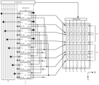
- a display device 1 has a display area (active area, AA area for short) and a peripheral area S. As shown in FIG. Wherein, the peripheral area S is located on at least one side of the display area. Exemplarily, the peripheral area S may be set around the display area AA.
- the display device 1 may include a plurality of sub-pixels P, each switch transistor is arranged corresponding to a sub-pixel P, the plurality of sub-pixels P are located in the AA area, and the plurality of sub-pixels P are arranged in an array in a row direction and a column direction.
- the sub-pixels P arranged in a row along the row direction may be referred to as pixels in the same row, and the sub-pixels P arranged in a row in the column direction may be referred to as pixels in the same row.
- the row direction is represented by X
- the column direction is represented by Y.
- each row of sub-pixels P includes a plurality of sub-pixels of a first color, a plurality of sub-pixels of a second color and a plurality of sub-pixels of a third color.
- first color, the second color and the third color which may be three primary colors or other colors.
- the first color, the second color, and the third color are blue, green, and red, respectively;
- each sub-pixel P may include: a pixel electrode 11 and a common electrode 12, and an electric field formed between the two is applied to the liquid crystal molecules corresponding to the sub-pixel P, so that the liquid crystal at the corresponding position of the sub-pixel P
- the molecules are arranged in a corresponding manner, thereby controlling the light output brightness of the sub-pixel P.
- the pixel electrode 11 and the common electrode 12 may both include a plurality of interconnected electrode strips with gaps between them, and the electrode strips belonging to the pixel electrode 11 and the electrode strips belonging to the common electrode 12 are arranged alternately; It includes a plurality of interconnected electrode strips with gaps between them, and the other is a flat electrode.
- the pixel electrode 11 and the common electrode 12 can be arranged in the same layer or in different layers.
- the display device 1 includes multiple gate lines GL and multiple data lines DL, and each sub-pixel is respectively coupled to one gate line GL and one data line DL. .
- the display device 1 also includes a scan drive circuit (Scan Drive IC) and a data drive circuit (Data Drive IC), and a timing control circuit (TCON IC) coupled to both the scan drive circuit and the data drive circuit.
- the timing control circuit is configured to convert the data signals and control signals received from the external interface into control signals suitable for the data drive circuit and the scan drive circuit, and output control signals such as RGB control signals to the data drive circuit, and to the scan drive circuit.
- the driving circuit outputs control signals such as a plurality of clock signals, thereby realizing image display of the display device.
- the scanning driving circuit can also be called a gate driving circuit (Gate Drive IC) or a column driving circuit (Row Drive IC).
- the scanning driving circuit is coupled to a plurality of gate lines GL. Scan signals are respectively output to the plurality of gate lines GL in accordance with the plurality of clock signals supplied from the timing control circuit.
- the plurality of gate lines GL are configured to respectively transmit scan signals to the plurality of sub-pixels P coupled thereto, so as to control the switching on and off of the switching transistors in the sub-pixels P.
- the data driving circuit can also be called a source driving circuit (Source Drive IC) or a row driving circuit (Column Drive IC).
- the data driving circuit is coupled to multiple data lines DL and is configured to send The data lines DL respectively output data signals.
- Each data line DL is configured to write a data signal into at least one (for example, one or more) sub-pixels P coupled thereto, and the data signal is the pixel data of the sub-pixel P (that is, enabling the sub-pixel
- the pixel displays the voltage value of the preset gray scale).
- the process of writing data signals into the sub-pixel P is the charging process of the load capacitor formed by the pixel electrode 11 and the common electrode 12 in the sub-pixel P. After the charging is completed, the voltage of the load capacitor is the gray scale voltage, and the gray scale voltage is is the subpixel data of this subpixel P.
- the scan driving circuit includes multiple rows of cascaded GOA units, respectively G1, G2, G3, G4...G(n-1), Gn, and each of the multiple cascaded GOA units All of them are correspondingly coupled to one gate line GL for realizing progressive scanning of the gate line GL.
- each GOA unit may include a signal input terminal Input, a signal output terminal Output, a reset signal terminal Reset, a clock signal terminal CLK, and a frame reset signal terminal Tot-Rst, etc., and the signal output terminal Output is correspondingly coupled to a gate line GL .
- the timing control circuit can input the frame reset signal STV0 to the frame reset signal terminal Tot-Rst of the multiple GOA units through the corresponding signal line, so as to reset the multiple GOA units before the start of each frame scanning period.
- the frame reset signal STV0 can reset multiple GOA units, so as to prevent the signal input to each GOA unit in the previous frame scanning period from interfering with the signals received by the GOA unit in the next frame scanning period, thereby eliminating possible adverse effects on the display effect Influence.
- the scan driving circuit can be coupled to the timing control circuit through a plurality of clock signal lines CL, each clock signal line CL is coupled to a plurality of GOA units, and is configured as a clock for the plurality of GOA units coupled to it.
- the signal terminals CLK respectively transmit the clock signal CLK.
- the specific setting method of the clock signal line CL which may be a 4CLK structure, a 6CLK structure, an 8CLK structure, a 12CLK structure, and the like.
- n GOA units are divided into k groups, and GOA units with intervals of k rows are divided into one group, that is, the 1st, 1+k, 1+2k... GOA units are taken as the first Group, take the 2nd, 2+k, 2+2k... GOA units as the second group, and so on until the k, 2k, 3k... GOA units are the kth Group.
- the signal output terminal Output of the mth GOA unit is connected to the signal input terminal Input of the m+kth GOA unit, and the signal output terminal Output of the m+kth GOA unit is connected to the mth GOA unit.
- the first GOA units of the first group to the kth group are respectively the first to the kth GOA units, and the other GOA units in each group are respectively cascaded after the signal output terminals of the first GOA units of each group, wherein k is a positive integer greater than or equal to 4, and both m and n are positive integers.
- the input signal of the signal input terminal Input of the GOA units G1, G2, G3, . . . Gk is the frame start signal STV.
- the n GOA units are divided into 4 groups, and the GOA units at intervals of 4 rows are divided into one group, and the 1st, 5th, 9th... GOA units are used as the first group, and the 1st GOA units are used as the first group. 2, 6, 10... GOA units are used as the second group, and so on until the 4th, 8, 12... GOA units are used as the 4th group.
- the input signal of the signal input terminal Input of G1, G2, G3 and G4 is the frame start signal STV
- the signal output terminal Output of G1 is connected to the signal input terminal Input of G5
- the signal output terminal Output of G2 is connected to G6
- Connect the signal output terminal Output of G3 to the signal input terminal Input of G7 connect the signal output terminal Output of G4 to the signal input terminal Input of G8, and at the same time, connect the signal output terminal Output of G5 to G1
- the reset signal terminal Reset of G6 connect the signal output terminal Output of G6 to the reset signal terminal Reset of G2, connect the signal output terminal Output of G7 to the reset signal terminal Reset of G3, connect the signal output terminal Output of G8 to the reset signal terminal of G4 Signal terminal Reset, and so on.
- the above scan driving circuit may also include a plurality of dummy GOA units (not shown in the figure), and there is no specific limitation on the number of dummy GOA units, as long as it is adjusted accordingly according to the number of dummy GOA units The signal connection relationship is sufficient.
- the internal structure of the virtual GOA unit is basically the same as that of the GOA unit, the difference is that the signal input terminals of each level of virtual GOA units are directly connected to the signal output terminals of the upper level virtual GOA unit.
- the virtual GOA units at all levels are mainly responsible for signal start-up, and play the role of signal trigger for the start-up of subsequent GOA units, and do not directly control the grid line scanning.
- the signal input terminal of the first-level virtual GOA unit inputs the frame start signal STV
- the signal output terminal of the last-level virtual GOA unit is connected to the signal input terminal of the first-level GOA unit G1.
- the display device may adopt double-sided driving, that is, the display device includes two scanning driving circuits arranged oppositely along the row direction (ie, the X direction), and the structures of the two scanning driving circuits are exactly the same. Both ends of each gate line GL are coupled to the two scan driving circuits located on the left and right sides respectively, and each signal terminal ( The signals respectively transmitted by the signal input terminal Input, the signal output terminal Output, the reset signal terminal Reset, the clock signal terminal CLK and the frame reset signal terminal Tot-Rst, etc.) are completely consistent.
- the degree of signal attenuation on the gate line GL can be alleviated to a certain extent.
- the effect of reducing signal attenuation is more prominent, thereby avoiding differences in display brightness at different positions in the display area AA, improving display uniformity, and improving display effects.
- the plurality of gate lines GL can be divided into a plurality of gate line groups GP, and each gate line group GP includes a plurality of gate lines GL, and the plurality of gate lines GL includes columns along the direction (ie Y direction) the first gate line GL1 , the second gate line GL2 and the third gate line GL3 arranged adjacently.
- the turn-on sequence of the gate lines GL is the first gate line GL1 , the second gate line GL2 and the third gate line GL3 .
- the display device may include a plurality of gate line groups GP, and each gate line group GP includes a first gate line GL1 , a second gate line GL2 and a third gate line GL3 arranged adjacently in a column direction.
- the display device includes a plurality of sub-pixels P arranged in an array. Any two adjacent sub-pixels P in the same row have different colors, and any adjacent two sub-pixels P in the same column have the same color.
- a gate line GL is provided between any two adjacent rows of sub-pixels P, and a plurality of gate lines GL arranged adjacently along the column direction form a plurality of gate line groups GP, and each gate line group GP includes The first gate line GL1 , the second gate line GL2 and the third gate line GL3 are provided.
- a plurality of sub-pixels P coupled to different gate lines GL are located in different rows, for example, referring to FIG. 3, a plurality of sub-pixels P coupled to the first gate line GL1, and a plurality of sub-pixels P coupled to the second gate line GL2 on different lines.
- the display device includes a plurality of sub-pixels P arranged in an array, any two adjacent sub-pixels P in the same row have different colors, any adjacent two sub-pixels P in the same column have the same color, and at least one (
- each data line DL may be coupled to two sub-pixels P in the same row, and the two sub-pixels P coupled to the same data line DL are respectively coupled to different gate lines GL, that is, a double gate line is adopted.
- GL Double Gate
- each gate line group GP includes the first gate line GL1, the second gate line GL2 and the third gate line GL3 arranged adjacently along the column direction, located along the Among the plurality of sub-pixels P between two adjacent gate lines GL in the column direction, some sub-pixels P are coupled to one of the two adjacent gate lines GL in the column direction, and the rest of the sub-pixels P are coupled to The other gate line GL of the two adjacent gate lines GL in the column direction is coupled.
- the application of double gate line technology can reduce the number of data lines DL in the display device by half, double the number of gate lines GL, correspondingly, the number of data driving circuits connected to the data lines DL is reduced by half, and The number of scan driving circuits connected to the gate lines GL is doubled. Since the unit price of the scan driving circuit is lower than that of the data driving circuit, the application of the double gate line GL technology is beneficial to cost control to a certain extent.
- the structure of the display device shown in FIG. 4 is taken as an example below to explain the embodiments of the present disclosure. It can be understood that the corresponding settings in any of the embodiments below can also be applied to In the display device shown in FIG. 3 , the same beneficial effect can be produced, and details will not be repeated here.
- the liquid crystal display device usually adopts a progressive scanning method to realize image display.
- the effective scanning period ET of the scanning signal SC transmitted by each gate line GL is are equal, the duration of the effective scanning period ET is T, and among any two adjacent gate lines GL along the column direction, the effective scanning period ET of the scanning signal SC transmitted by the gate line GL that outputs the scanning signal SC first
- the start time of the scanning signal SC transmitted by the gate line GL of the scanning signal SC is delayed for a fixed period T1, that is, the scanning period transmitted by any two adjacent gate lines GL along the column direction.
- the absolute values of the time differences between the start times of the active scanning period ET of the signal SC are equal, both being T1.
- the total time required to complete the progressive scanning of the three gate lines GL is T+2*T1.
- the scan driving circuit respectively outputting the scan signal SC to the plurality of gate lines GL includes: sequentially sending the scan signal SC to the first gate line GL1 Output the first scan signal SC1, output the second scan signal SC2 to the second gate line GL2, output the third scan signal SC3 to the third gate line GL3, the first scan signal SC1, the second scan signal SC2 and the third scan signal SC3
- the durations of the respective effective scanning periods ET are equal, both being T, and the starting moment of the effective scanning period ET of the second scanning signal SC2 is delayed by a first duration T1 compared with the starting moment of the effective scanning period ET of the first scanning signal SC1,
- the start time of the effective scan period ET of the third scan signal SC3 is delayed by a second time period T2 compared with the start time of the effective scan period ET of the second scan signal SC2 , and the second time period T2 is shorter than the first time period T1 .
- the duration of the voltage signal that can make the switch tube coupled to the gate line GL transmitting the scanning signal SC maintain an open state is the effective scanning period ET, and the duration of the duration is T.
- the start time of the effective scan period ET of the second scan signal SC2 is delayed by the first time length T1 compared with the start time of the effective scan period ET of the first scan signal SC1, that is, it is coupled with the first gate line GL1
- the plurality of switching transistors connected to the second gate line GL2 are turned on earlier than the plurality of switching transistors coupled to the second gate line GL2, and the plurality of switching transistors coupled to the second gate line GL2 and the plurality of switching transistors coupled to the first gate line GL1
- the time difference between the turn-on moment of the switch tube is the first duration T1
- the start moment of the effective scanning period ET of the third scanning signal SC3 is delayed by the second duration T2 compared with the starting moment of the effective scanning period ET of the second scanning signal SC2 , that is, the plurality of switching transistors coupled to the second gate line GL2 are turned on earlier than the plurality of switching transistors coupled to the third gate line GL3, and the plurality of switching transistors coupled to the third gate
- the first duration T1 is not greater than the duration of the effective scanning period ET of any scan signal SC.
- the first duration T1 can be equal to any scan signal SC. 1/3 of the effective scanning period ET of the SC.
- the duration of the effective scanning period ET of the scanning signal SC output by each gate line GL is also T
- the first duration is T1
- the second duration is T2
- the first gate line is completed.
- the total time required for the progressive scanning of GL1, the second grid line GL2 and the third grid line GL3 is T+T1+T2, which is compared with the total time required for the progressive scanning of the three grid lines T+ 2*T1, since T2 ⁇ T1, so T+T1+T2 ⁇ T+2*T1.
- the size of the second duration T2 is not too limited.
- the second duration T2 is zero, that is, the plurality of switching transistors coupled to the second gate line GL2 and the plurality of switching transistors coupled to the third gate line GL3 are turned on at the same time.
- the second duration T2 is greater than 0 and less than or equal to 1/2 of the first duration T1, and the number of switch tubes coupled to the second gate line GL2 is greater than the number of switch tubes coupled to the third gate line GL3.
- the switch tubes are turned on earlier, specifically, the time difference between the switch on times of the multiple switch tubes coupled to the third gate line GL3 and the multiple switch tubes coupled to the second gate line GL2 may be 1/1 of the first duration T1 2.
- the second duration T2 is shorter than the first duration T1. Therefore, similar to the above, when scanning multiple grid lines GL, the total duration required for the scanning process is reduced, and the above solutions can shorten the scanning of one frame. Cycle, increase the refresh rate.
- each At least part of the active scanning period ET overlaps.
- the scan driving circuit sequentially outputs the scan signal SC to the first gate line GL1, the second gate line GL2 and the third gate line GL3 arranged along the column direction in the gate line group GP, if the first scan signal SC1, the second gate line
- the effective scanning periods ET of the scanning signal SC2 and the third scanning signal SC3 do not overlap, and the first duration is T1 and the second duration is T2, the first gate line GL1, the second gate line GL2 and the third gate line are completed.
- the total time required for progressive scanning of GL3 is 3*T+T1+T2.
- the effective scanning periods ET of the first scanning signal SC1, the second scanning signal SC2, and the third scanning signal SC3 overlap, and the first duration is T1, and the second duration is T2, the completion
- the total time required for the progressive scanning of the first gate line GL1 , the second gate line GL2 and the third gate line GL3 is T+T1+T2.
- T+T1+T2 ⁇ 3*T+T1+T2 it can be seen that the above setting can further shorten the scanning period of one frame, thereby further improving the refresh rate and achieving better display effect.
- the clock signal line may adopt a 4CLK structure.
- the gate line group GP also includes a fourth gate line GL4 arranged adjacent to the third gate line GL3 in the column direction.
- the scan drive circuit outputs the fourth scan signal SC4 to the fourth gate line GL4, the start time of the effective scan period ET of the fourth scan signal SC4 is delayed by a third time period compared with the start time of the effective scan period ET of the third scan signal SC3 T3, wherein the third duration T3 is equal to the first duration T1.
- the second duration T2 is shorter than the first duration T1, which is equivalent to the early start of the effective scanning period ET of the second scanning signal SC2 transmitted by the second gate line GL2.
- the effective scanning period ET of the scanning signal SC of the gate lines GL also starts earlier, and the total time for the progressive scanning of the multiple gate lines will also be shortened, thereby having a shorter frame scanning period and a higher refresh rate.
- the use of fewer clock signal lines CL is beneficial to reduce the number of pins of the integrated circuit, reduce the frame of the display device, and enable users to obtain better visual experience.
- the scan driving circuit outputs the first scan signal SC1 and the fourth scan signal SC4 to the gate line group GP, At least part of the respective active scanning periods ET overlap. That is, within the effective scanning period ET of the first scanning signal SC1, the effective scanning period ET of the scanning signal SC transmitted by the second gate line GL2, the third gate line GL3 and the fourth gate line GL4 starts sequentially.
- the total time required for the scan driving circuit to output the scan signal SC to each gate line GL in one gate line group GP is shortened, and correspondingly completes a frame scan period for scanning each gate line GL in multiple gate line groups GP It is also shortened, which further increases the refresh rate and achieves a better display effect.
- the clock signal line CL can adopt an 8CLK structure.
- the plurality of gate line groups GP can include the first gate line group GP1 arranged adjacently in sequence along the column direction (ie, the Y direction). and the second grid line group.
- the GP2 is to divide any two adjacent grid line groups GP along the column direction into the first grid line group GP1 and the second grid line group GP2, and the first grid line group GP1 and the second grid line group GP2 each includes a first gate line GL1, a second gate line GL2, a third gate line GL3 and a fourth gate line GL4 arranged adjacently in sequence along the column direction, and the arrangement position of the first gate line group GP1 is at the Before GP2, in one frame scanning period, the effective scanning period ET of the scanning signal SC respectively outputted by the scanning driving circuit to each gate line GL in the second gate line group GP1 is shorter than that of the scanning signal SC output by the scanning driving circuit to the first gate line GL.
- the effective scanning period ET of the scanning signal SC output by each gate line GL in the group GP2 is delayed by a non-zero time length, and the effective scanning period ET of the scanning signal SC transmitted by each gate line GL in the first gate line group GP1
- the scanning period ET starts before the effective scanning period ET of the scanning signal SC transmitted by each gate line GL in the second gate line group GP2.
- the first gate line GL1 output in the second gate line GL2 group The starting moment of the effective scan period ET of the scan signal SC1 is delayed by a fourth time period T4.
- the fourth duration T4 is equal to the first duration T1. That is, in the first gate line group GL1, the start time of the effective scanning period ET of the fourth scanning signal SC4 transmitted by the fourth gate line GL4 is later than the fourth time period T4, and the first gate line in the second gate line group GP2 The effective scan period ET of the first scan signal SC1 transmitted by GL1 starts. Since the first gate line group GP1 and the second gate line group GP2 are only different in setting positions, the timing of the scanning signal SC transmitted by each gate line GL in the second gate line group GP2 is the same as that of each gate line GL in the first gate line group GP1.
- the timings of the scanning signals SC transmitted by the lines GL are similar, so the total time required to complete the scanning of each grid line GL in the second grid line group GP2 is also shortened.
- a frame scanning period of the display device of the line group GP2 can also be shortened, so as to have a higher refresh rate and a better display effect.
- using more clock signal lines to transmit clock signals can reduce the load on a single clock signal line, which is beneficial to reduce power consumption.
- the plurality of data lines DL includes a representative data line RL.
- a plurality of sub-pixels P coupled to a plurality of gate lines GL in one gate line group GP include: a first sub-pixel P1 coupled to a representative data line RL and a first gate line GL1, and a representative data line RL and a second sub-pixel P1
- the second sub-pixel P2 coupled to the gate line GL2 is the third sub-pixel P3 coupled to the representative data line RL and the third gate line GL3 , and the colors of the second sub-pixel P2 and the third sub-pixel P3 are the same.
- the first data signal D1 is written into the first sub-pixel P1 through the representative data line RL, and the second data signal is simultaneously written into the second sub-pixel P and the third sub-pixel P through the representative data line RL D2 or the third data signal D3;
- the first data signal D1 is the data signal corresponding to the pixel data of the first sub-pixel P1
- the second data signal D2 is the data signal corresponding to the pixel data of the second sub-pixel P2
- the third data signal D3 is a data signal corresponding to the pixel data of the third sub-pixel P3.
- the representative data line RL is any data line DL among the plurality of data lines DL.
- the data driving circuit needs to output the data signal three times.
- the data signal D2 or the third data signal D3 is sufficient, and the data driving circuit only needs to output the data signal twice to write data into the three sub-pixels P respectively coupled to the three gate lines GL. Since the number of output times of the data signal Data of the data driving circuit is reduced, the corresponding total time required for completing data writing is also reduced, which is beneficial to further shortening the scanning period of one frame and increasing the refresh rate.
- the second sub-pixel P2 and the third sub-pixel P3 are relatively close in space, and the colors of the second sub-pixel P2 and the third sub-pixel P3 are the same (that is, the second sub-pixel P2 and the third sub-pixel P3 are all red sub-pixels or blue sub-pixels or green sub-pixels), so the gray scales when the second sub-pixel P2 and the third sub-pixel P3 display images are also relatively close, so sharing the data signal of one of them for display is not only The improvement of the refresh rate can be realized, and a good display effect of the display device can be ensured.
- the second duration T2 is zero.
- the first data signal D1 is written into the first sub-pixel P1 through the representative data line RL, and the second data signal D2 is simultaneously written into the second sub-pixel P and the third sub-pixel P through the representative data line RL.
- the duration of the second data signal D2 is equal to the first duration T1, and the start time of the second data signal D2 is delayed by the fifth time length T5 compared with the start time of the effective scanning period ET of the second scan signal SC2, and the fifth time length T5 is the first 2 times as long as T1.
- the fifth time length T5 is the first 2 times as long as T1.
- the second duration T2 is zero
- the grid line group GP includes the first grid line GL1, the second grid line GL2, the third grid line GL3 and the fourth grid line GL4, and a grid line group
- the plurality of sub-pixels P coupled to the plurality of gate lines GL in the GP also includes a fourth sub-pixel P4 coupled to the representative data line RL and the fourth gate line GL4, and writes to the fourth sub-pixel P4 through the representative data line RL.
- the fourth data signal D4, the fourth data signal D4 is a data signal corresponding to the pixel data of the fourth sub-pixel P4.
- the specific timing of the first data signal D1 and the fourth data signal D4 is not limited too much. For example, referring to FIG. 9 and FIG.
- the second data signal D2 is simultaneously written in the second sub-pixel P2 and the third sub-pixel P3, and the duration of the first data signal D1, the second data signal D2 and the fourth data signal D4
- the durations are all equal to the first duration T1
- the duration of the time difference between the start moment of the first data signal D1 and the start moment of the effective scanning period of the first scan signal SC1 is equal to twice the first duration T1
- the duration of the fourth data signal D4 The duration of the time difference between the start moment and the start moment of the effective scan period ET of the fourth scan signal SC4 is also equal to twice the first duration T1 .
- the start time of the second data signal D2 is delayed by a fifth time period T5 compared with the start time of the effective scan period ET of the second scan signal SC2 , and the fifth time period T5 is twice the first time period T1 .
- the duration of the time difference between the start moment of the third data signal SC3 and the start moment of the effective scan period ET of the third scan signal SC3 is also equal to twice the first duration T1 .
- the second duration T2 is zero
- the first data signal D1 can be written into the first sub-pixel P1 through the representative data line RL
- the first data signal D1 can be written into the first sub-pixel P1 through the representative data line.
- the second sub-pixel P2 and the third sub-pixel P3 write the third data signal D3 at the same time.
- the duration of the third data signal D3 is equal to the first duration T1
- the start moment of the third data signal D3 is delayed by the fifth duration T5 compared to the start timing of the effective scanning period ET of the third scan signal SC3, and the fifth duration T5 is the first duration T5. 2 times as long as T1. Similar to the above, this setting also has a shorter data writing time and can also time a higher refresh rate.
- the second duration T2 is not zero.
- the scanning of the third gate line GL3 is started in advance, and it is also possible to simultaneously write to the second sub-pixel P and the third sub-pixel P through the representative data line RL. Input the second data signal D2. Similar to the foregoing, the reduction in the writing times of the data signal Data can also shorten the scan period and increase the refresh rate.
- the second duration T2 is greater than 0 and less than or equal to 1/2 of the first duration T1 .
- the first data signal D1 is written into the first sub-pixel P1 through the representative data line RL
- the second data signal is simultaneously written into the second sub-pixel P2 and the third sub-pixel P3 through the representative data line RL D2
- the end time of the second data signal D2 is earlier than the end time of the effective scan period ET of the third scan signal SC3 by a sixth time period T6.
- the first data signal D1 is written into the first sub-pixel P1 through the representative data line RL, and the second sub-pixel P2 and the third sub-pixel P3 are written through the representative data line RL.
- the third data signal D3 is written, and the end moment of the third data signal D3 is delayed by the seventh time period T7 compared with the end moment of the effective scan period ET of the second scan signal SC2 .
- the durations of the second data signal D2 and the third data signal D3 are both equal to the first duration T1, and both the sixth duration T6 and the seventh duration T7 are greater than zero.
- the image display process of the display device includes a multi-frame scanning period, which can be divided into an odd-numbered frame scanning period and an even-numbered frame scanning period.
- the timing control circuit inputs odd numbers to the scanning drive circuit.
- the frame start signal STVA when the scan period is an even frame scan period, the timing control circuit inputs the even frame start signal STVB to the scan driving circuit.
- this setting method can write data line numbers into the second sub-pixel P2 and the third sub-pixel P3 through a data writing process, and can also reduce the number of data signals Data output by the data driving circuit in one frame scanning period. The number of times, therefore, also has the aforementioned beneficial effects, and will not be repeated here.
- the second duration T2 is greater than 0 and less than or equal to 1/2 of the first duration T1
- the first data signal D1 is written, and the third data signal D3 is simultaneously written to the second sub-pixel P2 and the third sub-pixel P3 through the representative data line RL.
- the end time of the third data signal D3 is compared with that of the second scanning signal SC2
- the end moment of the effective scanning period ET is delayed by a seventh time period T7.
- the first data signal D1 is written into the first sub-pixel P1 through the representative data line RL, and the second sub-pixel P2 and the third sub-pixel P3 are written through the representative data line RL.
- the second data signal D2 is written, and the end time of the second data signal D2 is earlier than the end time of the effective scan period ET of the third scan signal SC3 by a sixth time length T6.
- the durations of the second data signal D2 and the third data signal D3 are both equal to the first duration T1, and both the sixth duration T6 and the seventh duration T7 are greater than zero. It can also reduce the number of writes and achieve a higher refresh rate.
- the specific value of the second duration is not too limited.
- the second duration T2 is equal to 1/2 of the first duration T1 .
- the first duration T1 can be 1/3 of the duration of the effective scanning period ET of any scanning signal SC
- the duration of the second duration T2 can be 1/3 of the duration of the effective scanning period ET of any scanning signal SC.
- the durations of the second data signal D2 and the third data signal D3 are both equal to the first duration T1
- both the sixth duration T6 and the seventh duration T7 are 1/2 of the first duration T1.
- the start moment of the second data signal D2 is delayed by an eighth time period T8 compared to the start moment of the effective scan period ET of the second scan signal SC2 .
- the start moment of the third data signal D3 is delayed by a ninth time period T9 compared to the start moment of the effective scan period ET of the third scan signal SC3 .
- Both the eighth duration T8 and the ninth duration T9 are twice the first duration. Referring to Fig. 10, Fig. 11 and Fig.
- the second duration T2 is equal to 1/2 of the first duration
- the gate line group GP includes the first gate line GL1, the second gate line GL2, the third gate line GL3 and the fourth gate line GL4, a plurality of sub-pixels P coupled to a plurality of gate lines GL in one gate line group GP also includes a fourth sub-pixel P4 coupled to a representative data line RL and a fourth gate line GL4, through the representative data line RL to A fourth data signal D4 is written into the fourth sub-pixel P4, and the fourth data signal D4 is a data signal corresponding to the pixel data of the fourth sub-pixel P4.
- the specific timing of the first data signal D1 and the fourth data signal D4 is not limited too much.
- the durations of the first data signal D1, the second data signal D2 and the fourth data signal D4 are all equal to the first duration T1 and the start time of the first data signal D1 is the same as the effective scanning period of the first scanning signal SC1
- the duration of the time difference between the start moments of ET is equal to twice the first duration T1
- the duration of the time difference between the start moment of the fourth data signal D4 and the start moment of the effective scanning period ET of the fourth scan signal SC4 is also equal to the first duration 2 times of T1.
- the start moment of the second data signal D2 is delayed by an eighth time length T8 compared to the start time of the effective scan period ET of the second scan signal SC2, and the eighth time length T8 is equal to the first time period T8. Twice the time length T1, the end time of the second data signal D2 is earlier than the end time of the effective scanning period ET of the third scanning signal SC3 by the sixth time length T6, and the sixth time length T6 is 1/2 of the first time length T1 .
- the duration of the time difference between the start moment of the third data signal D3 and the start moment of the effective scan period ET of the second scan signal SC2 is equal to 2.5 times the first duration T1
- the ending moment of the third data signal D3 is delayed by the seventh duration T7 compared with the ending moment of the effective scanning period ET of the second scanning signal SC2, and the seventh duration T7 is 1/2 of the first duration T1
- the third data signal D3 The start time is delayed by a ninth time period T9 compared with the start time of the effective scan period ET of the third scan signal SC3 , and the ninth time period T9 is twice the first time period T1 .
- the data signal Data can be written into the multiple sub-pixels P of the second sub-pixel P2 and the third sub-pixel P3 only through one writing process, and the writing times of the data signal Data are reduced.
- the total time required for data to be written into Data is reduced, which is beneficial to further shortening the scanning period of one frame and improving the refresh rate.
- any two adjacent grid lines GL along the column direction in the first grid line GL1 group are divided into the previous grid line GL and the subsequent grid line GL, and the position of the previous grid line GL is set at the position of the subsequent grid line.
- the effective scan period of the scan signal output by the scan drive circuit to the subsequent gate line is delayed by a non-zero value compared with the effective scan period of the scan signal output by the scan drive circuit to the previous gate line. duration.
- the setting position of the first grid line GL1 is before the second grid line GL2, then for the first grid line GL1 and the second grid line GL2, the first grid line
- the line GL1 is a preceding gate line
- the second gate line GL2 is a subsequent gate line.
- the setting position of the second gate line GL2 is before the third gate line GL3, then for the second gate line GL2 and the third gate line GL3, the second gate line GL2
- the second gate line GL2 is the previous gate line
- the third gate line GL3 is the subsequent gate line.
- the preceding grid line and the following grid line are relative concepts, and do not specifically refer to a certain grid line.
- the liquid crystal display device when the refresh rate of the liquid crystal display device is high, the problem of insufficient charging of the load capacitor is likely to occur.
- each data line DL is configured to respectively write a data signal into each sub-pixel of at least one (for example, three) sub-pixel row
- the data signals respectively written into the respective sub-pixels coupled to the preceding gate line partially overlap with the effective scanning period of the scanning signal output by the scanning driving circuit to the subsequent gate line.
- the effective scan period of the scan signal output by the scan drive circuit to the previous gate line partially overlaps with the effective scan period of the scan signal output by the scan drive circuit to the subsequent gate line, so that each of the scan signals coupled to the previous gate line
- the switching transistors corresponding to the sub-pixels are turned on, the switching transistors corresponding to the respective sub-pixels coupled to the previous gate lines are also turned on.
- the data signals respectively written in the respective sub-pixels coupled with the previous gate line partially overlap with the effective scan period of the scan signal output by the scan drive circuit to the subsequent gate line, then the pair coupled with the previous gate line While charging the load capacitance of each connected sub-pixel, the data signal of each sub-pixel coupled with the previous gate line can be respectively written into each sub-pixel coupled with the subsequent gate line, so as to be connected with the subsequent gate line.
- the load capacitors of the line-coupled sub-pixels are precharged.
- the difference between the gray-scale voltage of the current frame of the sub-pixel and the pre-charge voltage is smaller than the gray-scale voltage of the current frame of the sub-pixel and the gray-scale voltage of the previous frame, so in the current frame, some The pixel is pre-charged, which shortens the time required for the sub-pixel to reach the gray scale voltage, avoids the problem of insufficient charging of the load capacitor, and is conducive to the increase of the refresh rate.
- the respective effective scanning periods ET of the first scanning signal SC1 and the second scanning signal SC2 partially overlap, and the data signal Data written in the first sub-pixel P1 It overlaps with the part of the effective scanning period ET in the second scanning signal SC2, so that while the first sub-pixel P1 is being charged, the row of the second sub-pixel P2 can be pre-charged, thereby shortening the time period corresponding to the second sub-pixel P2.
- the charging time of the load capacitor is beneficial to improve the refresh rate.
- the gate line group GP also includes the fourth gate line GL4, the first scan signal SC1, the second scan signal SC2, the third scan signal
- the respective effective scanning periods ET of SC3 and the fourth scanning signal SC4 partially overlap, and the respective effective scanning periods ET of the first data signal D1 and the second scanning signal SC2, the third scanning signal SC3 and the fourth scanning signal SC4 partially overlap.
- the respective sub-pixels P coupled to the first gate line GL1 are being charged respectively
- the respective sub-pixels P coupled to the second gate line GL2 , the third gate line GL3 and the fourth gate line GL4 can be respectively charged.
- Precharging is performed, thereby shortening the time required for the four sub-pixels P to reach the gray-scale voltage, and having a higher refresh rate and better display effect.
- the data signal of the liquid crystal display device changes positively and negatively based on the common voltage.
- the driving signal is positive, otherwise it is negative. If a positive polarity data signal is charged into a sub-pixel, the sub-pixel is of positive polarity; if a negative polarity data signal is charged into a sub-pixel, then the sub-pixel is of negative polarity.
- the polarity of the input data signal is different, its luminous brightness is different. For example, referring to FIG.
- the plurality of data lines DL includes first data lines DL1 and second data lines DL2 alternately distributed along the row direction (ie, the X direction).
- the data driving circuit is configured to output the first type of data signal to the first data line DL1, and output the second type of data signal to the second data line DL, wherein the first type of data signal and the second type of data signal
- the polarity of the data signal is different.
- the first data line DL1 outputs the first type of data signal
- the polarity of the first type of data signal is positive
- the second data line DL2 outputs the second type of data signal, the polarity of the second type of data signal for negative polarity.
- the above-mentioned data signal Data input method makes the polarities of multiple sub-pixels P of the same color in the same column (that is, the Y direction) the same, and among the multiple sub-pixels P of the same color in any two adjacent columns, one of them
- the polarity of multiple sub-pixels P in one column is different from that of multiple sub-pixels P in another column, so that in one frame scanning period, multiple columns of sub-pixels P with the same color but different polarities can average the brightness in the row direction, achieving a relatively Uniform display brightness.
- the setting method of the data line DL and the data signal Data transmitted by it is similar to the above.
- the above-mentioned data signal input method makes the polarities of multiple sub-pixels P of the same color in the same column different, and they are located in the same column.
- a plurality of sub-pixels P of the same color in a row also have different polarities.
- the polarities of multiple sub-pixels P with the same color in the same row are arranged repeatedly as positive, negative and negative, and the polarities of multiple sub-pixels P with the same color in the same column are alternately arranged as positive and negative, so that
- the data signal input method of column inversion can be used to achieve a display effect similar to dot inversion.
- the average brightness can be achieved in the row and column directions, and a better display effect can be achieved. .
- the liquid crystal display device can be driven by driving methods such as row inversion (Row inversion), column inversion (Column inversion), and dot inversion (Dot inversion), so as to avoid physical damage of liquid crystal molecules.
- driving methods such as row inversion (Row inversion), column inversion (Column inversion), and dot inversion (Dot inversion), so as to avoid physical damage of liquid crystal molecules.
- Row inversion Row inversion
- Column inversion Column inversion
- Dot inversion dot inversion
- the problem of solidification of characteristics occurs, so as to achieve better display effect and prolong the service life of equipment.
- a column inversion driving manner may be adopted, and the polarities of the data signals output by the data driving circuit to the same data signal are different in two adjacent frame scanning periods.
- a method for driving a display device is provided.
- the driving method may be executed by the above-mentioned display device, or may be a product including the above-mentioned display device.
- the driving method includes: in one frame scanning period, the scanning driving circuit is configured to output the scanning signal SC to the plurality of gate lines GL in the gate line group GP, specifically, scanning The driving circuit sequentially outputs the first scan signal SC1 to the first gate line GL1 , outputs the second scan signal SC2 to the second gate line GL2 , and outputs the third scan signal SC3 to the third gate line GL3 .
- the effective scanning period ET of the first scanning signal SC1, the second scanning signal SC2 and the third scanning signal SC3 have the same duration, and the start time of the effective scanning period ET of the second scanning signal SC2 is shorter than that of the first scanning signal SC2.
- the starting moment of the effective scanning period ET of SC1 is delayed by the first duration T1
- the starting moment of the effective scanning period ET of the third scanning signal SC3 is delayed by the second duration T2 compared with the starting moment of the effective scanning period ET of the second scanning signal SC2,
- the second duration T2 is shorter than the first duration T1.
- the first duration T1 is not greater than the duration of the effective scanning period ET of any scan signal SC.
- the first duration T1 can be equal to any scan signal SC.
- this driving method is equivalent to advancing the effective scanning period ET of the third scanning signal SC3 by a second time period T2, and the overall timing of the scanning signal SC output after the third scanning signal SC3 is also advanced, so that in When the progressive scanning of multiple gate lines GL is performed, the total time required to complete a frame scanning period is shorter, which is conducive to achieving a higher refresh rate and better display effect.
- the second duration T2 there is no excessive limitation on the specific duration (ie, the second duration T2 ) in which the start time of the effective scanning period ET of the third scanning signal SC3 is advanced.
- the second duration T2 may be zero, and for another example, the second duration T2 may be greater than 0 and less than or equal to 1/2 of the first duration T1.
- the use of the driving method can also achieve the purpose of increasing the refresh rate and improving the display effect.
- the display device 1 when the display device 1 further includes a data driving circuit and a plurality of data lines DL, the data driving circuit is coupled to the plurality of data lines DL and is configured to provide data to the plurality of data lines DL.
- the lines DL respectively output data signals Data
- the data lines DL are configured to write the data signals Data into the sub-pixels P
- the data signals Data are pixel data of the sub-pixels P.
- the plurality of data lines DL include representative data lines RL
- the plurality of sub-pixels P coupled to the plurality of gate lines GL in one gate line group GP include: a first sub-pixel coupled to the representative data line RL and the first gate line GL1 Pixel P1, the second sub-pixel P2 coupled with the representative data line RL and the second gate line GL2, the third sub-pixel P3 coupled with the representative data line RL and the third gate line GL3, the second sub-pixel P2 and the second The three sub-pixels P3 have the same color.
- the driving method of the display device also includes that in a frame scanning period, the data driving circuit writes the first data signal D1 to the second sub-pixel P2 through the representative data line RL, and writes the first data signal D1 to the second sub-pixel P2 through the representative data line RL.
- the pixel P2 and the third sub-pixel P3 write the second data signal D2 or the third data signal D3 at the same time;
- the first data signal D1 is the data signal corresponding to the pixel data of the first sub-pixel P1
- the second data signal D2 is the second The data signal corresponding to the pixel data of the sub-pixel P2
- the third data signal D3 is a data signal corresponding to the pixel data of the third sub-pixel P3.
- the representative data line RL is any data line DL among the plurality of data lines DL. According to the above-mentioned driving method, the output times of the data signal of the data driving circuit are reduced, and correspondingly the total time required for completing data writing is also reduced, which is beneficial to further shorten the scanning period of one frame and improve the refresh rate.
- the plurality of data lines DL includes first data lines DL1 and second data lines DL2 alternately distributed along the row direction (ie, the X direction).
- the data driving circuit outputs the first type of data signal to the first data line DL1, and outputs the second type of data signal to the second data line DL2, wherein the first type of data signal and the second type of data signal
- the polarity is different. This setting enables the multiple columns of sub-pixels P with the same color but different polarities to perform luminance averaging in the row and column directions during the display process of a frame of image, so that the display luminance is relatively uniform, thereby achieving better display effect.
- Some embodiments of the present disclosure provide a computer-readable storage medium (for example, a non-transitory computer-readable storage medium), in which computer program instructions are stored, and the computer program instructions are stored in a computer (for example, a liquid crystal When running on the display device), the computer is made to execute the driving method of the display device as described in any one of the above embodiments.
- a computer-readable storage medium for example, a non-transitory computer-readable storage medium
- the computer program instructions are stored in a computer (for example, a liquid crystal When running on the display device), the computer is made to execute the driving method of the display device as described in any one of the above embodiments.
- the above-mentioned computer-readable storage medium may include, but is not limited to: a magnetic storage device (for example, a hard disk, a floppy disk, or a magnetic tape, etc.), an optical disk (for example, a CD (Compact Disk, a compact disk), a DVD (Digital Versatile Disk, Digital Versatile Disk), etc.), smart cards and flash memory devices (for example, EPROM (Erasable Programmable Read-Only Memory, Erasable Programmable Read-Only Memory), card, stick or key drive, etc.).
- Various computer-readable storage media described in this disclosure can represent one or more devices and/or other machine-readable storage media for storing information.
- the term "machine-readable storage medium" may include, but is not limited to, wireless channels and various other media capable of storing, containing and/or carrying instructions and/or data.
- Some embodiments of the present disclosure also provide a computer program product.
- the computer program product includes computer program instructions.
- the computer program instructions When the computer program instructions are executed on a computer (eg, a liquid crystal display device), the computer program instructions cause the computer to execute the method for driving the display device as described in the above embodiments.
- Some embodiments of the present disclosure also provide a computer program.
- the computer program When the computer program is executed on a computer (for example, a liquid crystal display device), the computer program causes the computer to execute the method for driving the display device as described in the above-mentioned embodiments.
Landscapes
- Engineering & Computer Science (AREA)
- Physics & Mathematics (AREA)
- Computer Hardware Design (AREA)
- General Physics & Mathematics (AREA)
- Theoretical Computer Science (AREA)
- Chemical & Material Sciences (AREA)
- Crystallography & Structural Chemistry (AREA)
- Control Of Indicators Other Than Cathode Ray Tubes (AREA)
Abstract
Description
本申请要求于2021年8月18日提交的、申请号为202110948612.3的中国专利申请的优先权,其全部内容通过引用结合在本申请中。This application claims priority to a Chinese patent application with application number 202110948612.3 filed on August 18, 2021, the entire contents of which are incorporated herein by reference.
本公开涉及显示技术领域,尤其涉及一种显示装置及其驱动方法。The present disclosure relates to the field of display technology, and in particular, to a display device and a driving method thereof.
液晶显示装置(Liquid Crystal Display,简称为LCD)由于具有体积小、功耗低、无辐射、显示分辨率高等特点,已开始大量普及并逐渐成为主流产品。Liquid Crystal Display (Liquid Crystal Display, LCD for short) has begun to be widely popularized and gradually become a mainstream product due to its characteristics of small size, low power consumption, no radiation, and high display resolution.
发明内容Contents of the invention
一方面,提供一种显示装置,所述显示装置包括:多个子像素,所述多个子像素阵列排布;至少一个栅线组,所述栅线组包括多条栅线,所述多条栅线包括:沿列方向依次相邻设置的第一栅线、第二栅线和第三栅线;扫描驱动电路,所述扫描驱动电路与所述栅线组中的多条栅线耦接,被配置为在一个帧扫描周期中,向所述栅线组中的所述多条栅线分别输出扫描信号,包括:依次向所述第一栅线输出第一扫描信号,向所述第二栅线输出第二扫描信号,向所述第三栅线输出第三扫描信号;其中,所述第一扫描信号、所述第二扫描信号和所述第三扫描信号各自的有效扫描时段的时长相等,且所述第二扫描信号的有效扫描时段的开始时刻相较于所述第一扫描信号的有效扫描时段的开始时刻延迟第一时长,所述第三扫描信号的有效扫描时段的开始时刻相较于所述第二扫描信号的有效扫描时段的开始时刻延迟第二时长;所述第二时长小于所述第一时长。In one aspect, a display device is provided, the display device includes: a plurality of sub-pixels arranged in an array; at least one gate line group, the gate line group includes a plurality of gate lines, and the plurality of gate lines The lines include: a first gate line, a second gate line and a third gate line arranged adjacently in sequence along the column direction; a scanning driving circuit, the scanning driving circuit is coupled to a plurality of gate lines in the gate line group, It is configured to respectively output scan signals to the plurality of gate lines in the gate line group in a frame scan period, including: sequentially outputting a first scan signal to the first gate line, and outputting a first scan signal to the second gate line in sequence. The gate line outputs a second scan signal, and outputs a third scan signal to the third gate line; wherein, the duration of the effective scan period of each of the first scan signal, the second scan signal and the third scan signal are equal, and the start moment of the effective scan period of the second scan signal is delayed by a first duration compared with the start moment of the effective scan period of the first scan signal, and the start moment of the effective scan period of the third scan signal The starting moment of the effective scanning period of the second scanning signal is delayed by a second duration; the second duration is shorter than the first duration.
在一些实施例中,所述第二时长为零。In some embodiments, the second duration is zero.
在一些实施例中,所述第二时长大于0且小于等于所述第一时长的1/2。In some embodiments, the second duration is greater than 0 and less than or equal to 1/2 of the first duration.
在一些实施例中,所述扫描驱动电路向所述栅线组中沿所述列方向任意相邻的两条栅线分别输出的扫描信号中,各自的有效扫描时段至少部分重叠。In some embodiments, in the scan signals respectively output by the scan driving circuit to any two adjacent gate lines in the gate line group along the column direction, respective valid scan periods overlap at least partially.
在一些实施例中,所述栅线组还包括:与所述第三栅线沿所述列方向相邻设置的第四栅线;所述扫描驱动电路被配置为向所述第四栅线输出第四扫描信号,所述第四扫描信号和所述第三扫描信号各自的有效扫描时段的时长相等,所述第四扫描信号的有效扫描时段的开始时刻相较于所述第三扫描信号的有效扫描时段的开始时刻延迟第三时长,所述第三时长与所述第一时长相等。In some embodiments, the gate line group further includes: a fourth gate line adjacent to the third gate line along the column direction; the scan driving circuit is configured to Outputting a fourth scanning signal, the duration of the effective scanning periods of the fourth scanning signal and the third scanning signal are equal, and the start time of the effective scanning period of the fourth scanning signal is compared with that of the third scanning signal The starting moment of the effective scanning period of the delay is a third time length, and the third time length is equal to the first time length.
在一些实施例中,所述扫描驱动电路向所述栅线组输出的所述第一扫描信号和所述第四扫描信号,各自的有效扫描时段部分重叠。In some embodiments, the effective scanning periods of the first scanning signal and the fourth scanning signal output by the scanning driving circuit to the gate line group partially overlap.
在一些实施例中,所述至少一个栅线组包括沿所述列方向依次相邻设置的第一栅线组和第二栅线组;相较于所述第一栅线组中第四栅线输出的第四扫描信号的有效扫描时段的开始时刻,所述第二栅线组中第一栅线输出的第一扫描信号的有效扫描时段的开始时刻延迟第四时长;所述第四时长与所述第一时长相等。In some embodiments, the at least one grid line group includes a first grid line group and a second grid line group arranged adjacently in sequence along the column direction; compared with the fourth grid line group in the first grid line group The starting moment of the effective scanning period of the fourth scanning signal output by the line, the starting moment of the effective scanning period of the first scanning signal output by the first gate line in the second gate line group is delayed by a fourth time length; the fourth time length equal to the first duration.
在一些实施例中,所述的显示装置还包括:数据驱动电路和多条数据线,所述数据驱动电路与所述多条数据线耦接,被配置为向所述多条数据线分别输出数据信号,所述数据线被配置为向子像素写入数据信号,所述数据信号为所述子像素的子像素数据;所述多条数据线包括代表数据线;与一个栅线组中的多条栅线耦接的多个子像素包括:与所述代表数据线和所述第一栅线耦接的第一子像素,与所述代表数据线和所述第二栅线耦接的第二子像素,与所述代表数据线和所述第三栅线耦接的第三子像素;所述第二子像素和所述第三子像素颜色相同;在一个帧扫描周期中,通过所述代表数据线向所述第二子像素写入第一数据信号,通过所述代表数据线向所述第二子像素和所述第三子像素同时写入第二数据信号或第三数据信号;所述第一数据信号是所述第一子像素的像素数据对应的数据信号,所述第二数据信号是所述第二子像素的像素数据对应的数据信号,所述第三数据信号是所述第三子像素的像素数据对应的数据信号。In some embodiments, the display device further includes: a data driving circuit and a plurality of data lines, the data driving circuit is coupled to the plurality of data lines, and is configured to respectively output Data signal, the data line is configured to write the data signal to the sub-pixel, the data signal is the sub-pixel data of the sub-pixel; the plurality of data lines include a representative data line; The multiple sub-pixels coupled with multiple gate lines include: a first sub-pixel coupled with the representative data line and the first gate line, a first sub-pixel coupled with the representative data line and the second gate line Two sub-pixels, the third sub-pixel coupled to the representative data line and the third gate line; the second sub-pixel and the third sub-pixel have the same color; in one frame scanning period, through the The representative data line writes the first data signal to the second sub-pixel, and simultaneously writes the second data signal or the third data signal to the second sub-pixel and the third sub-pixel through the representative data line ; The first data signal is a data signal corresponding to the pixel data of the first sub-pixel, the second data signal is a data signal corresponding to the pixel data of the second sub-pixel, and the third data signal is A data signal corresponding to the pixel data of the third sub-pixel.
在一些实施例中,在一个帧扫描周期中,所述第二时长为零;通过所述代表数据线向所述第一子像素写入所述第一数据信号,通过所述代表数据线向所述第二子像素和所述第三子像素同时写入所述第二数据信号;所述第二数据信号的持续时长等于所述第一时长;所述第二数据信号的开始时刻相较于所述第二扫描信号的有效扫描时段的开始时刻延迟第五时长;所述第五时长为所述第一时长的2倍。In some embodiments, in one frame scanning period, the second duration is zero; the first data signal is written to the first sub-pixel through the representative data line, and the first data signal is written to the first sub-pixel through the representative data line. The second subpixel and the third subpixel write the second data signal at the same time; the duration of the second data signal is equal to the first duration; the start time of the second data signal is compared with A fifth duration is delayed from the beginning of the effective scanning period of the second scanning signal; the fifth duration is twice the first duration.
在一些实施例中,所述第二时长大于0且小于等于所述第一时长的1/2;在奇数帧扫描周期中,通过所述代表数据线向所述第一子像素写入所述第一数据信号,通过所述代表数据线向所述第二子像素和所述第三子像素同时写入所述第二数据信号,所述第二数据信号的结束时刻相较于所述第三扫描信号的的结束时刻提前第六时长;在偶数帧扫描周期中,通过所述代表数据线向所述第一子像素写入所述第一数据信号,通过所述代表数据线向所述第二子像素和所述第三子像素同时写入所述第三数据信号,所述第三数据信号的 结束时刻相较于所述第二扫描信号的有效扫描时段的结束时刻延迟第七时长;所述第二数据信号和所述第三数据信号的持续时长均等于所述第一时长;所述第六时长和所述第七时长均大于0。In some embodiments, the second duration is greater than 0 and less than or equal to 1/2 of the first duration; in an odd frame scanning period, the representative data line is used to write the The first data signal, the second data signal is simultaneously written to the second sub-pixel and the third sub-pixel through the representative data line, and the end time of the second data signal is compared with that of the first The end time of the three-scanning signal is advanced by the sixth duration; in the even-numbered frame scanning period, the first data signal is written to the first sub-pixel through the representative data line, and the first data signal is written to the first sub-pixel through the representative data line. The second sub-pixel and the third sub-pixel write the third data signal at the same time, and the end time of the third data signal is delayed by a seventh time period compared with the end time of the effective scanning period of the second scan signal ; The durations of the second data signal and the third data signal are both equal to the first duration; the sixth duration and the seventh duration are both greater than 0.
在一些实施例中,所述第二时长等于所述第一时长的1/2;所述第二数据信号和所述第三数据信号的持续时长均等于所述第一时长;所述第六时长和所述第七时长均为所述第一时长的1/2;在奇数帧扫描周期中,所述第二数据信号的开始时刻相较于所述第二扫描信号的有效扫描时段的开始时刻延迟第八时长;在偶数帧扫描周期中,所述第三数据信号的开始时刻相较于所述第三扫描信号的有效扫描时段的开始时刻延迟第九时长;所述第八时长和所述第九时长均为所述第一时长的2倍。In some embodiments, the second duration is equal to 1/2 of the first duration; the durations of the second data signal and the third data signal are both equal to the first duration; the sixth Both the duration and the seventh duration are 1/2 of the first duration; in the odd frame scan period, the start moment of the second data signal is compared to the start of the effective scan period of the second scan signal The timing is delayed by an eighth duration; in the even frame scanning period, the start moment of the third data signal is delayed by the ninth duration compared with the start moment of the effective scanning period of the third scan signal; the eighth duration and the The ninth duration is twice the first duration.
在一些实施例中,所述扫描驱动电路向所述第一栅线组中沿所述列方向任意相邻的两条栅线分别输出的扫描信号中,各自的有效扫描时段至少部分重叠;所述第一栅线组中沿所述列方向任意相邻的所述两条栅线分为在先栅线和在后栅线,所述在先栅线的位置设置在所述在后栅线之前;分别写入与所述在先栅线耦接的各个子像素中的数据信号,与所述扫描驱动电路向所述在后栅线输出的扫描信号的有效扫描时段部分重叠。In some embodiments, in the scan signals respectively output by the scan driving circuit to any two adjacent gate lines in the first gate line group along the column direction, the effective scan periods of each are at least partially overlapped; The two adjacent grid lines in the first grid line group along the column direction are divided into a previous grid line and a subsequent grid line, and the position of the previous grid line is set at the position of the subsequent grid line. Before: the data signals respectively written into the respective sub-pixels coupled to the preceding gate line partially overlap with the effective scanning period of the scanning signal output by the scanning drive circuit to the subsequent gate line.
在一些实施例中,所述多条数据线包括沿行方向交替分布的第一数据线和第二数据线;在一帧扫描周期中,所述数据驱动电路被配置为向所述第一数据线输出第一类数据信号,向所述第二数据线输出第二类数据信号;其中,所述第一类数据信号和所述第二类数据信号的极性不同。In some embodiments, the plurality of data lines include first data lines and second data lines alternately distributed along the row direction; The first type of data signal is output to the second data line, and the second type of data signal is output to the second data line; wherein, the polarity of the first type of data signal and the second type of data signal are different.
在一些实施例中,一数据线与同一行中的两个子像素耦接,与所述数据线耦接的所述两个子像素分别耦接至不同的栅线。In some embodiments, a data line is coupled to two sub-pixels in the same row, and the two sub-pixels coupled to the data line are respectively coupled to different gate lines.
在一些实施例中,所述的显示装置还包括:时序控制电路,所述时序控制电路与所述扫描驱动电路耦接,被配置为向所述扫描驱动电路输出多个时钟信号;所述扫描驱动电路被配置为根据所述多个时钟信号,向所述多条栅线分别输出扫描信号。In some embodiments, the display device further includes: a timing control circuit, coupled to the scanning driving circuit, configured to output a plurality of clock signals to the scanning driving circuit; the scanning The driving circuit is configured to respectively output scan signals to the plurality of gate lines according to the plurality of clock signals.
另一方面,提供一种显示装置的驱动方法,其中,所述显示装置如前述任一实施例所述,所述驱动方法包括:在一帧扫描周期中,所述扫描驱动电路被配置为向所述栅线组中的所述多条栅线分别输出扫描信号,包括:依次向所述第一栅线输出第一扫描信号,向所述第二栅线输出第二扫描信号,向所述第三栅线输出第三扫描信号;其中,所述第一扫描信号、所述第二扫描信号和所述第三扫描信号各自的有效扫描时段的时长相等,且所述第二扫描信号的有效扫描时段相较于所述第一扫描信号的有效扫描时段的开始时刻延 迟第一时长,所述第三扫描信号的有效扫描时段的开始时刻相较于所述第二扫描信号的有效扫描时段的开始时刻延迟第二时长;所述第二时长小于所述第一时长。In another aspect, a method for driving a display device is provided, wherein the display device is as described in any one of the foregoing embodiments, and the method includes: in a frame scanning period, the scanning driving circuit is configured to The plurality of gate lines in the gate line group respectively output scan signals, including: sequentially outputting a first scan signal to the first gate line, outputting a second scan signal to the second gate line, and outputting a second scan signal to the second gate line; The third gate line outputs a third scanning signal; wherein, the effective scanning periods of the first scanning signal, the second scanning signal and the third scanning signal have the same duration, and the effective scanning period of the second scanning signal The scan period is delayed by a first duration compared to the start time of the effective scan period of the first scan signal, and the start time of the effective scan period of the third scan signal is compared with the start time of the effective scan period of the second scan signal The start moment is delayed by a second duration; the second duration is shorter than the first duration.
在一些实施例中,所述显示装置还包括:数据驱动电路和多条数据线,所述数据驱动电路与所述多条数据线耦接,被配置为向所述多条数据线分别输出数据信号,所述数据线被配置为向子像素写入数据信号,所述数据信号为所述子像素的子像素数据;所述多条数据线包括代表数据线;与一个栅线组中的多条栅线耦接的多个子像素包括:与所述代表数据线和所述第一栅线耦接的第一子像素,与所述代表数据线和所述第二栅线耦接的第二子像素,与所述代表数据线和所述第三栅线耦接的第三子像素;所述第二子像素和所述第三子像素颜色相同;所述驱动方法还包括:在一个帧扫描周期中,所述数据驱动电路通过所述代表数据线向所述第二子像素写入第一数据信号,通过所述代表数据线向所述第二子像素和所述第三子像素同时写入第二数据信号或第三数据信号;所述第一数据信号是所述第一子像素的像素数据对应的数据信号,所述第二数据信号是所述第二子像素的像素数据对应的数据信号,所述第三数据信号是所述第三子像素的像素数据对应的数据信号。In some embodiments, the display device further includes: a data driving circuit and a plurality of data lines, the data driving circuit is coupled to the plurality of data lines, and is configured to output data to the plurality of data lines respectively signal, the data line is configured to write a data signal to the sub-pixel, the data signal is the sub-pixel data of the sub-pixel; the plurality of data lines include a representative data line; The multiple sub-pixels coupled with the gate lines include: a first sub-pixel coupled with the representative data line and the first gate line, a second sub-pixel coupled with the representative data line and the second gate line A sub-pixel, a third sub-pixel coupled to the representative data line and the third gate line; the second sub-pixel and the third sub-pixel have the same color; the driving method further includes: During the scanning period, the data drive circuit writes the first data signal to the second sub-pixel through the representative data line, and simultaneously writes the first data signal to the second sub-pixel and the third sub-pixel through the representative data line. Writing a second data signal or a third data signal; the first data signal is a data signal corresponding to the pixel data of the first sub-pixel, and the second data signal is a data signal corresponding to the pixel data of the second sub-pixel data signal, the third data signal is a data signal corresponding to the pixel data of the third sub-pixel.
在一些实施例中,所述多条数据线包括沿行方向相邻设置的第一数据线和第二数据线,所述驱动方法还包括:在一帧扫描周期中,所述数据驱动电路向所述第一数据线输出第一类数据信号,向所述第二数据线输出第二类数据信号;其中,所述第一类数据信号和所述第二类数据信号的极性不同。In some embodiments, the plurality of data lines include a first data line and a second data line adjacently arranged along the row direction, and the driving method further includes: during a frame scanning period, the data driving circuit sends The first data line outputs a first-type data signal, and outputs a second-type data signal to the second data line; wherein, the first-type data signal and the second-type data signal have different polarities.
为了更清楚地说明本公开中的技术方案,下面将对本公开一些实施例中所需要使用的附图作简单地介绍,显而易见地,下面描述中的附图仅仅是本公开的一些实施例的附图,对于本领域普通技术人员来讲,还可以根据这些附图获得其他的附图。此外,以下描述中的附图可以视作示意图,并非对本公开实施例所涉及的产品的实际尺寸、方法的实际流程、信号的实际时序等的限制。In order to illustrate the technical solutions in the present disclosure more clearly, the following will briefly introduce the accompanying drawings used in some embodiments of the present disclosure. Apparently, the accompanying drawings in the following description are only appendices to some embodiments of the present disclosure. Figures, for those of ordinary skill in the art, other drawings can also be obtained based on these drawings. In addition, the drawings in the following description can be regarded as schematic diagrams, and are not limitations on the actual size of the product involved in the embodiments of the present disclosure, the actual process of the method, the actual timing of signals, and the like.
图1为根据一些实施例的显示装置的结构图;FIG. 1 is a structural diagram of a display device according to some embodiments;
图2为根据另一些实施例的显示装置的结构图;Fig. 2 is a structural diagram of a display device according to other embodiments;
图3为根据另一些实施例的显示装置的结构图;Fig. 3 is a structural diagram of a display device according to other embodiments;
图4为根据又一些实施例的显示装置的结构图;Fig. 4 is a structural diagram of a display device according to still other embodiments;
图5为根据一些实施例的扫描信号的时序图;5 is a timing diagram of scan signals according to some embodiments;
图6为根据另一些实施例的扫描信号的时序图;FIG. 6 is a timing diagram of scanning signals according to other embodiments;
图7为根据又一些实施例的扫描信号的时序图;FIG. 7 is a timing diagram of scanning signals according to still other embodiments;
图8为根据另一些实施例的显示装置的结构图;Fig. 8 is a structural diagram of a display device according to other embodiments;
图9为根据一些实施例的扫描信号和数据信号的时序图;9 is a timing diagram of scan signals and data signals according to some embodiments;
图10为根据另一些实施例的扫描信号和数据信号的时序图;FIG. 10 is a timing diagram of scan signals and data signals according to other embodiments;
图11为根据又一些实施例的扫描信号和数据信号的时序图;FIG. 11 is a timing diagram of scan signals and data signals according to still other embodiments;
图12为根据另一些实施例的显示装置的结构图。Fig. 12 is a structural diagram of a display device according to some other embodiments.
下面将结合附图,对本公开一些实施例中的技术方案进行清楚、完整地描述,显然,所描述的实施例仅仅是本公开一部分实施例,而不是全部的实施例。基于本公开所提供的实施例,本领域普通技术人员所获得的所有其他实施例,都属于本公开保护的范围。The technical solutions in some embodiments of the present disclosure will be clearly and completely described below in conjunction with the accompanying drawings. Apparently, the described embodiments are only some of the embodiments of the present disclosure, not all of them. All other embodiments obtained by persons of ordinary skill in the art based on the embodiments provided in the present disclosure belong to the protection scope of the present disclosure.
除非上下文另有要求,否则,在整个说明书和权利要求书中,术语“包括(comprise)”及其其他形式例如第三人称单数形式“包括(comprises)”和现在分词形式“包括(comprising)”被解释为开放、包含的意思,即为“包含,但不限于”。在说明书的描述中,术语“一个实施例(one embodiment)”、“一些实施例(some embodiments)”、“示例性实施例(exemplary embodiments)”、“示例(example)”、“特定示例(specific example)”或“一些示例(some examples)”等旨在表明与该实施例或示例相关的特定特征、结构、材料或特性包括在本公开的至少一个实施例或示例中。上述术语的示意性表示不一定是指同一实施例或示例。此外,所述的特定特征、结构、材料或特点可以以任何适当方式包括在任何一个或多个实施例或示例中。Throughout the specification and claims, unless the context requires otherwise, the term "comprise" and other forms such as the third person singular "comprises" and the present participle "comprising" are used Interpreted as the meaning of openness and inclusion, that is, "including, but not limited to". In the description of the specification, the terms "one embodiment", "some embodiments", "exemplary embodiments", "example", "specific examples" example)" or "some examples (some examples)" etc. are intended to indicate that specific features, structures, materials or characteristics related to the embodiment or examples are included in at least one embodiment or example of the present disclosure. Schematic representations of the above terms are not necessarily referring to the same embodiment or example. Furthermore, the particular features, structures, materials or characteristics described may be included in any suitable manner in any one or more embodiments or examples.
以下,术语“第一”、“第二”仅用于描述目的,而不能理解为指示或暗示相对重要性或者隐含指明所指示的技术特征的数量。由此,限定有“第一”、“第二”的特征可以明示或者隐含地包括一个或者更多个该特征。在本公开实施例的描述中,除非另有说明,“多个”的含义是两个或两个以上。Hereinafter, the terms "first" and "second" are used for descriptive purposes only, and cannot be understood as indicating or implying relative importance or implicitly specifying the quantity of indicated technical features. Thus, a feature defined as "first" and "second" may explicitly or implicitly include one or more of these features. In the description of the embodiments of the present disclosure, unless otherwise specified, "plurality" means two or more.
在描述一些实施例时,可能使用了“耦接”和“连接”及其衍伸的表达。例如,描述一些实施例时可能使用了术语“连接”以表明两个或两个以上部件彼此间有直接物理接触或电接触。又如,描述一些实施例时可能使用了术语“耦接”以表明两个或两个以上部件有直接物理接触或电接触。然而,术语“耦接”或“通信耦合(communicatively coupled)”也可能指两个或两个以上部件彼此间并无直接接触,但仍彼此协作或相互作用。这里所公开的实施例并不必然限制于本文内容。In describing some embodiments, the expressions "coupled" and "connected" and their derivatives may be used. For example, the term "connected" may be used in describing some embodiments to indicate that two or more elements are in direct physical or electrical contact with each other. As another example, the term "coupled" may be used when describing some embodiments to indicate that two or more elements are in direct physical or electrical contact. However, the terms "coupled" or "communicatively coupled" may also mean that two or more elements are not in direct contact with each other, but yet still co-operate or interact with each other. The embodiments disclosed herein are not necessarily limited by the context herein.
本文中“适用于”或“被配置为”的使用意味着开放和包容性的语言, 其不排除适用于或被配置为执行额外任务或步骤的设备。另外,“基于”的使用意味着开放和包容性,因为“基于”一个或多个所述条件或值的过程、步骤、计算或其他动作在实践中可以基于额外条件或超出所述的值。The use of "suitable for" or "configured to" herein means open and inclusive language that does not exclude devices that are suitable for or configured to perform additional tasks or steps. Additionally, the use of "based on" is meant to be open and inclusive, as a process, step, calculation, or other action that is "based on" one or more stated conditions or values may in practice be based on additional conditions or beyond stated values.
本文参照作为理想化示例性附图的剖视图和/或平面图描述了示例性实施方式。在附图中,为了清楚,放大了层和区域的厚度。因此,可设想到由于例如制造技术和/或公差引起的相对于附图的形状的变动。因此,示例性实施方式不应解释为局限于本文示出的区域的形状,而是包括因例如制造而引起的形状偏差。例如,示为矩形的蚀刻区域通常将具有弯曲的特征。因此,附图中所示的区域本质上是示意性的,且它们的形状并非旨在示出设备的区域的实际形状,并且并非旨在限制示例性实施方式的范围。Exemplary embodiments are described herein with reference to cross-sectional and/or plan views that are idealized exemplary drawings. In the drawings, the thickness of layers and regions are exaggerated for clarity. Accordingly, variations in shape from the drawings as a result, for example, of manufacturing techniques and/or tolerances are contemplated. Thus, example embodiments should not be construed as limited to the shapes of regions illustrated herein but are to include deviations in shapes that result, for example, from manufacturing. For example, an etched region illustrated as a rectangle will, typically, have curved features. Thus, the regions illustrated in the figures are schematic in nature and their shapes are not intended to illustrate the actual shape of a region of a device and are not intended to limit the scope of example embodiments.
液晶显示装置中包括多条栅线和多条数据线,以及由多条栅线和多条数据线交叉界定的多个子像素,每个子像素与一条栅线和一条数据线分别耦接,栅线被配置为向与其耦接的子像素传输扫描信号,数据线被配置为向与其耦接的子像素传输数据信号。液晶显示装置还包括多个开关管(例如,薄膜晶体管,Thin Film Transistor,简称为TFT),每个开关管与一个子像素对应设置。相关技术中,液晶显示装置通常采用逐行扫描的方式实现图像显示。在进行逐行扫描时,首先,首行的栅线向与其耦接的多个子像素输出扫描信号,使得多个子像素的开关晶体管处于开启状态,数据线向首行的多个子像素输出数据信号,之后,第二行的栅线向与其耦接的多个子像素输出扫描信号,同时首行的扫描信号输出停止,数据线向第二行的多个子像素输出数据信号,以此类推。随着液晶显示技术的发展,对液晶显示装置的显示效果要求也越来越高,而当液晶显示装置能够达到的刷新频率越大时,图像显示的闪烁程度就越小,显示图像的画面质量就越高,因此如何提高液晶显示装置的刷新频率,成为亟待解决的问题。The liquid crystal display device includes a plurality of gate lines and a plurality of data lines, and a plurality of sub-pixels defined by intersections of the plurality of gate lines and a plurality of data lines, each sub-pixel is respectively coupled to a gate line and a data line, and the gate line The data lines are configured to transmit scan signals to the sub-pixels coupled thereto, and the data lines are configured to transmit data signals to the sub-pixels coupled thereto. The liquid crystal display device also includes a plurality of switch tubes (for example, Thin Film Transistor, Thin Film Transistor, referred to as TFT), and each switch tube is set corresponding to a sub-pixel. In the related art, liquid crystal display devices generally implement image display in a progressive scanning manner. When performing row-by-row scanning, firstly, the gate line of the first row outputs a scan signal to a plurality of sub-pixels coupled thereto, so that the switching transistors of the plurality of sub-pixels are in an on state, and the data line outputs a data signal to a plurality of sub-pixels of the first row, Afterwards, the gate lines in the second row output scan signals to the multiple sub-pixels coupled thereto, while the scan signal output in the first row stops, the data lines output data signals to the multiple sub-pixels in the second row, and so on. With the development of liquid crystal display technology, the requirements for the display effect of liquid crystal display devices are getting higher and higher, and when the refresh rate that the liquid crystal display device can achieve is higher, the flickering degree of the image display will be smaller, and the picture quality of the displayed image will be lower. Therefore, how to increase the refresh rate of the liquid crystal display device becomes an urgent problem to be solved.
为了解决上述问题,本公开的一些实施例提供了一种显示装置。显示装置被配置为显示图像;例如,可以显示静态图像或动态图像等。示例性地,该显示装置可以是液晶显示面板,也可以是包括液晶显示面板和驱动电路(驱动电路与液晶显示面板耦接,被配置为驱动液晶显示面板显示图像)的产品。具体的,液晶显示面板可以是AD-SDS(Advanced-Super Dimensional Switching,高级超维场开关技术)型液晶显示面板,也可以是IPS(In Plane Switch,平面转换)型液晶显示面板。由于液晶分子仅对光线进行调制,自身并不能发光,因此为了实现图像显示,示例性地,该产品还可以包括:设置于液晶显示面板的背面(背离显示面的一侧)的背光模组,该背光模组被配 置为向液晶显示面板提供背光。对背光模组的类型不作过多限制,例如,可以为侧入式背光模组,也可以为直下式背光模组。In order to solve the above problems, some embodiments of the present disclosure provide a display device. The display device is configured to display an image; for example, a still image or a moving image or the like may be displayed. Exemplarily, the display device may be a liquid crystal display panel, or a product including a liquid crystal display panel and a driving circuit (the driving circuit is coupled to the liquid crystal display panel and configured to drive the liquid crystal display panel to display images). Specifically, the liquid crystal display panel may be an AD-SDS (Advanced-Super Dimensional Switching, advanced super-dimensional field switching technology) type liquid crystal display panel, or an IPS (In Plane Switch, in-plane switching) type liquid crystal display panel. Since liquid crystal molecules only modulate light and cannot emit light by themselves, in order to realize image display, for example, the product may also include: a backlight module disposed on the back of the liquid crystal display panel (the side away from the display surface), The backlight module is configured to provide backlight to the liquid crystal display panel. The type of the backlight module is not limited too much, for example, it may be an edge-type backlight module or a direct-type backlight module.
示例性地,上述产品可以是:显示器,电视,广告牌,数码相框,具有显示功能的激光打印机,电话,手机,个人数字助理(Personal Digital Assistant,PDA),数码相机,便携式摄录机,取景器,导航仪,车用显示装置,拼接显示装置,家电,信息查询设备(如电子政务、银行、医院、电力等部门的业务查询设备),监视器等。Exemplarily, the above-mentioned products may be: monitors, televisions, billboards, digital photo frames, laser printers with display functions, telephones, mobile phones, personal digital assistants (Personal Digital Assistant, PDA), digital cameras, camcorders, viewfinders Devices, navigators, car display devices, splicing display devices, home appliances, information query equipment (such as business query equipment for e-government, banks, hospitals, electric power and other departments), monitors, etc.
在本公开的一些实施例中,参见图1,显示装置1具有显示区(active area,简称AA区)和周边区S。其中,周边区S位于显示区至少一侧。示例性地,周边区S可以围绕显示区AA一圈设置。显示装置1可以包括多个子像素P,每个开关管与一个子像素P对应设置,多个子像素P位于AA区,多个子像素P按行方向和列方向阵列排布。具体的,沿行方向排列成一排的子像素P可以称为同一行像素,沿列方向排列成一排的子像素P可以称为同一列像素。其中,行方向用X表示,列方向用Y表示。In some embodiments of the present disclosure, referring to FIG. 1 , a
示例性地,每行子像素P包括多个第一颜色子像素、多个第二颜色子像素和多个第三颜色子像素。对第一颜色、第二颜色和第三颜色不做限制,可以为三基色,也可以为其他颜色。例如,第一颜色、第二颜色和第三颜色分别为蓝色、绿色和红色;即,参见图1,多个子像素包括蓝色子像素B、绿色子像素G和红色子像素R。Exemplarily, each row of sub-pixels P includes a plurality of sub-pixels of a first color, a plurality of sub-pixels of a second color and a plurality of sub-pixels of a third color. There is no limitation on the first color, the second color and the third color, which may be three primary colors or other colors. For example, the first color, the second color, and the third color are blue, green, and red, respectively;
继续参见图1,每个子像素P可以包括:像素电极11和公共电极12,二者之间形成的电场施加给与该子像素P相对应的液晶分子,使得该子像素P对应位置处的液晶分子呈相应的排列方式,从而控制该子像素P的出光亮度。本公开中对像素电极11和公共电极12的具体形状以及相对位置设置不做过多限制。例如,像素电极11和公共电极12可以均包括多个相互连接、彼此之间有缝隙的电极条,且属于像素电极11的电极条与属于公共电极12的电极条交替设置;也可以是一者包括多个相互连接、彼此之间有缝隙的电极条,另一者为平板电极。像素电极11和公共电极12可以同层设置,也可以不同层设置。Continuing to refer to FIG. 1, each sub-pixel P may include: a
在本公开的一些实施例中,参见图1,与前述类似的,显示装置1包括多条栅线GL和多条数据线DL,每个子像素与一条栅线GL和一条数据线DL分别耦接。显示装置1还包括扫描驱动电路(Scan Drive IC)和数据驱动电路(Data Drive IC),以及与扫描驱动电路和数据驱动电路均耦接的时序控制电路(TCON IC)。其中,时序控制电路被配置为将从外部接口接收到的数据 信号和控制信号转换成适合于数据驱动电路和扫描驱动电路的控制信号,并向数据驱动电路输出RGB控制信号等控制信号,向扫描驱动电路输出多个时钟信号等控制信号,从而实现显示装置的图像显示。扫描驱动电路也可称为栅极驱动电路(Gate Drive IC)或者列驱动电路(Row Drive IC),扫描驱动电路与多条栅线GL耦接,在一帧扫描周期中,扫描驱动电路被配置为根据时序控制电路提供的多个时钟信号,向多条栅线GL分别输出扫描信号。多条栅线GL被配置为向与其耦接的多个子像素P分别传输扫描信号,以控制子像素P中开关管的开启与关闭。数据驱动电路也可称为源极驱动电路(Source Drive IC)或者行驱动电路(Column Drive IC),数据驱动电路与多条数据线DL耦接,被配置为在开关管打开后,向各条数据线DL分别输出数据信号。每条数据线DL被配置为向与其耦接的至少一个(例如,可以是一个或多个)子像素P中写入数据信号,该数据信号即为子像素P的像素数据(即能使子像素显示预设灰阶的电压值)。子像素P写入数据信号的过程即为子像素P中像素电极11和公共电极12所形成的负荷电容的充电过程,在充电结束后,负荷电容的电压为灰阶电压,该灰阶电压即为这个子像素P的子像素数据。In some embodiments of the present disclosure, referring to FIG. 1 , similar to the foregoing, the
示例性地,参见图2,扫描驱动电路包括多行级联的GOA单元,分别为G1、G2、G3、G4…G(n-1)、Gn,级联的多个GOA单元中的每个均与一条栅线GL对应耦接,用于实现栅线GL的逐行扫描。具体的,每个GOA单元可以包括信号输入端Input、信号输出端Output、复位信号端Reset、时钟信号端CLK和帧复位信号端Tot-Rst等,信号输出端Output与一条栅线GL对应耦接。其中,时序控制电路可以通过相应的信号线向多个GOA单元的帧复位信号端Tot-Rst输入帧复位信号STV0,以在每个帧扫描周期开始之前对多个GOA单元进行复位。帧复位信号STV0可使多个GOA单元进行复位,从而避免前一个帧扫描周期输入各GOA单元的信号对GOA单元接收后一个帧扫描周期的各信号造成干扰,从而消除可能对显示效果造成的不良影响。Exemplarily, referring to FIG. 2 , the scan driving circuit includes multiple rows of cascaded GOA units, respectively G1, G2, G3, G4...G(n-1), Gn, and each of the multiple cascaded GOA units All of them are correspondingly coupled to one gate line GL for realizing progressive scanning of the gate line GL. Specifically, each GOA unit may include a signal input terminal Input, a signal output terminal Output, a reset signal terminal Reset, a clock signal terminal CLK, and a frame reset signal terminal Tot-Rst, etc., and the signal output terminal Output is correspondingly coupled to a gate line GL . Wherein, the timing control circuit can input the frame reset signal STV0 to the frame reset signal terminal Tot-Rst of the multiple GOA units through the corresponding signal line, so as to reset the multiple GOA units before the start of each frame scanning period. The frame reset signal STV0 can reset multiple GOA units, so as to prevent the signal input to each GOA unit in the previous frame scanning period from interfering with the signals received by the GOA unit in the next frame scanning period, thereby eliminating possible adverse effects on the display effect Influence.
示例性地,扫描驱动电路可以通过多条时钟信号线CL与时序控制电路耦接,每条时钟信号线CL与多个GOA单元耦接,被配置为向与其耦接的多个GOA单元的时钟信号端CLK分别传输时钟信号CLK。具体的,对时钟信号线CL的具体设置方式不做过多限制,可以为4CLK结构、6CLK结构、8CLK结构、12CLK结构等。Exemplarily, the scan driving circuit can be coupled to the timing control circuit through a plurality of clock signal lines CL, each clock signal line CL is coupled to a plurality of GOA units, and is configured as a clock for the plurality of GOA units coupled to it. The signal terminals CLK respectively transmit the clock signal CLK. Specifically, there are no too many restrictions on the specific setting method of the clock signal line CL, which may be a 4CLK structure, a 6CLK structure, an 8CLK structure, a 12CLK structure, and the like.
示例性地,将n个GOA单元分为k组,将间隔k行的GOA单元分为一组,也即将第1、1+k、1+2k......个GOA单元作为第一组,将第2、2+k、2+2k......个GOA单元作为第二组,依此类推,直至第k、2k、3k......个GOA单元作为 第k组。其中,将第m个GOA单元的信号输出端Output连接至第m+k个GOA单元的信号输入端Input,并将第m+k个GOA单元的信号输出端Output连接至第m个GOA单元的复位信号端Reset,依此类推,以实现GOA单元的级联。第1组至第k组的第1个GOA单元分别为第1个至第k个GOA单元,各组内其他GOA单元分别级联在各组的第1个GOA单元的信号输出端之后,其中k为大于等于4的正整数,m和n均为正整数。在整个扫描驱动电路中,GOA单元G1、G2、G3、……Gk的信号输入端Input的输入信号是帧起始信号STV。例如,参见图2,将n个GOA单元分为4组,每间隔4行的GOA单元分为一组,第1、5、9......个GOA单元作为第一组,将第2、6、10......个GOA单元作为第二组,依此类推,直至第4、8、12......个GOA单元作为第4组。其中,G1、G2、G3和G4的信号输入端Input的输入信号是帧起始信号STV,将G1的信号输出端Output连接至G5的信号输入端Input,将G2的信号输出端Output连接至G6的信号输入端Input,将G3的信号输出端Output连接至G7的信号输入端Input,将G4的信号输出端Output连接至G8的信号输入端Input,同时,将G5的信号输出端Output连接至G1的复位信号端Reset,将G6的信号输出端Output连接至G2的复位信号端Reset,将G7的信号输出端Output连接至G3的复位信号端Reset,将G8的信号输出端Output连接至G4的复位信号端Reset,依此类推。Exemplarily, n GOA units are divided into k groups, and GOA units with intervals of k rows are divided into one group, that is, the 1st, 1+k, 1+2k... GOA units are taken as the first Group, take the 2nd, 2+k, 2+2k... GOA units as the second group, and so on until the k, 2k, 3k... GOA units are the kth Group. Among them, the signal output terminal Output of the mth GOA unit is connected to the signal input terminal Input of the m+kth GOA unit, and the signal output terminal Output of the m+kth GOA unit is connected to the mth GOA unit. Reset signal terminal Reset, and so on, to realize the cascading of GOA units. The first GOA units of the first group to the kth group are respectively the first to the kth GOA units, and the other GOA units in each group are respectively cascaded after the signal output terminals of the first GOA units of each group, wherein k is a positive integer greater than or equal to 4, and both m and n are positive integers. In the entire scan driving circuit, the input signal of the signal input terminal Input of the GOA units G1, G2, G3, . . . Gk is the frame start signal STV. For example, referring to Figure 2, the n GOA units are divided into 4 groups, and the GOA units at intervals of 4 rows are divided into one group, and the 1st, 5th, 9th... GOA units are used as the first group, and the 1st GOA units are used as the first group. 2, 6, 10... GOA units are used as the second group, and so on until the 4th, 8, 12... GOA units are used as the 4th group. Among them, the input signal of the signal input terminal Input of G1, G2, G3 and G4 is the frame start signal STV, the signal output terminal Output of G1 is connected to the signal input terminal Input of G5, and the signal output terminal Output of G2 is connected to G6 Connect the signal output terminal Output of G3 to the signal input terminal Input of G7, connect the signal output terminal Output of G4 to the signal input terminal Input of G8, and at the same time, connect the signal output terminal Output of G5 to G1 The reset signal terminal Reset of G6, connect the signal output terminal Output of G6 to the reset signal terminal Reset of G2, connect the signal output terminal Output of G7 to the reset signal terminal Reset of G3, connect the signal output terminal Output of G8 to the reset signal terminal of G4 Signal terminal Reset, and so on.
示例性地,上述的扫描驱动电路还可以包括多个虚拟(Dummy)GOA单元(图中未示出),对虚拟GOA单元的个数不作具体限制,只要根据虚拟GOA单元的个数相应地调整信号连接关系即可。虚拟GOA单元与GOA单元的内部结构基本相同,区别在于各级虚拟GOA单元的信号输入端直接连接上一级虚拟GOA单元的信号输出端。各级虚拟GOA单元主要负责信号启动,为后续GOA单元的开启起到信号触发的作用,不对栅线扫描进行直接控制。具体的,第一级虚拟GOA单元的信号输入端输入帧起始信号STV,最后一级虚拟GOA单元的信号输出端连接到第一级GOA单元G1的信号输入端。Exemplarily, the above scan driving circuit may also include a plurality of dummy GOA units (not shown in the figure), and there is no specific limitation on the number of dummy GOA units, as long as it is adjusted accordingly according to the number of dummy GOA units The signal connection relationship is sufficient. The internal structure of the virtual GOA unit is basically the same as that of the GOA unit, the difference is that the signal input terminals of each level of virtual GOA units are directly connected to the signal output terminals of the upper level virtual GOA unit. The virtual GOA units at all levels are mainly responsible for signal start-up, and play the role of signal trigger for the start-up of subsequent GOA units, and do not directly control the grid line scanning. Specifically, the signal input terminal of the first-level virtual GOA unit inputs the frame start signal STV, and the signal output terminal of the last-level virtual GOA unit is connected to the signal input terminal of the first-level GOA unit G1.
示例性地,参见图3,显示装置可以采用双边驱动,即显示装置包括两个沿行方向(即X方向)相对设置的扫描驱动电路,两个扫描驱动电路的结构完全一致。每条栅线GL的两端与分别位于左侧和右侧的两个扫描驱动电路均耦接,且与同一条栅线GL耦接的两个扫描驱动电路中的GOA单元的各个信号端(包括信号输入端Input、信号输出端Output、复位信号端Reset、时钟信号端CLK和帧复位信号端Tot-Rst等)所分别传输的信号完全一致。这样一来,由于每条栅线GL所传输的扫描信号从这条栅线GL的两端分别输入,能 够在一定程度上减轻该栅线GL上的信号衰减程度。对于中大尺寸的显示装置而言,降低信号衰减的效果更为突出,从而避免显示区AA中不同位置处的显示亮度等存在差异,提高显示的均一化,提升显示效果。For example, referring to FIG. 3 , the display device may adopt double-sided driving, that is, the display device includes two scanning driving circuits arranged oppositely along the row direction (ie, the X direction), and the structures of the two scanning driving circuits are exactly the same. Both ends of each gate line GL are coupled to the two scan driving circuits located on the left and right sides respectively, and each signal terminal ( The signals respectively transmitted by the signal input terminal Input, the signal output terminal Output, the reset signal terminal Reset, the clock signal terminal CLK and the frame reset signal terminal Tot-Rst, etc.) are completely consistent. In this way, since the scanning signal transmitted by each gate line GL is respectively input from both ends of the gate line GL, the degree of signal attenuation on the gate line GL can be alleviated to a certain extent. For medium and large-sized display devices, the effect of reducing signal attenuation is more prominent, thereby avoiding differences in display brightness at different positions in the display area AA, improving display uniformity, and improving display effects.
示例性地,参见图3和图4,多条栅线GL可以划分为多个栅线组GP,每个栅线组GP包括多条栅线GL,多条栅线GL包括沿列方向(即Y方向)相邻设置的第一栅线GL1、第二栅线GL2和第三栅线GL3。在进行逐行扫描时,栅线GL的开启顺序依次为第一栅线GL1、第二栅线GL2和第三栅线GL3。显示装置可以包括多个栅线组GP,每个栅线组GP中均包括沿列方向相邻设置的第一栅线GL1、第二栅线GL2和第三栅线GL3。Exemplarily, referring to FIG. 3 and FIG. 4 , the plurality of gate lines GL can be divided into a plurality of gate line groups GP, and each gate line group GP includes a plurality of gate lines GL, and the plurality of gate lines GL includes columns along the direction (ie Y direction) the first gate line GL1 , the second gate line GL2 and the third gate line GL3 arranged adjacently. During progressive scanning, the turn-on sequence of the gate lines GL is the first gate line GL1 , the second gate line GL2 and the third gate line GL3 . The display device may include a plurality of gate line groups GP, and each gate line group GP includes a first gate line GL1 , a second gate line GL2 and a third gate line GL3 arranged adjacently in a column direction.
例如,参见图3,显示装置包括阵列排布的多个子像素P,同一行中任意相邻的两个子像素P颜色不同,同一列中任意相邻的两个子像素P颜色相同,沿列方向相邻设置的任意两行子像素P之间设置有一条栅线GL,沿列方向相邻设置的多条栅线GL形成多个栅线组GP,每个栅线组GP包括沿列方向相邻设置的第一栅线GL1、第二栅线GL2和第三栅线GL3。与不同栅线GL耦接的多个子像素P位于不同行,例如,参见图3,与第一栅线GL1耦接的多个子像素P,和与第二栅线GL2耦接的多个子像素P位于不同行。For example, referring to FIG. 3 , the display device includes a plurality of sub-pixels P arranged in an array. Any two adjacent sub-pixels P in the same row have different colors, and any adjacent two sub-pixels P in the same column have the same color. A gate line GL is provided between any two adjacent rows of sub-pixels P, and a plurality of gate lines GL arranged adjacently along the column direction form a plurality of gate line groups GP, and each gate line group GP includes The first gate line GL1 , the second gate line GL2 and the third gate line GL3 are provided. A plurality of sub-pixels P coupled to different gate lines GL are located in different rows, for example, referring to FIG. 3, a plurality of sub-pixels P coupled to the first gate line GL1, and a plurality of sub-pixels P coupled to the second gate line GL2 on different lines.
又例如,参见图4,显示装置包括阵列排布的多个子像素P,同一行中任意相邻的两个子像素P颜色不同,同一列中任意相邻的两个子像素P颜色相同,至少一条(例如,可以是每条)数据线DL与同一行中的两个子像素P耦接,与同一条数据线DL耦接的两个子像素P分别耦接至不同的栅线GL,即采用双栅线GL(Dual Gate)技术。其中,沿列方向相邻设置有多个栅线组GP,每个栅线组GP包括沿列方向相邻设置的第一栅线GL1、第二栅线GL2和第三栅线GL3,位于沿列方向相邻的两条栅线GL之间的多个子像素P中,一部分子像素P与沿列方向相邻的两条栅线GL中的一条栅线GL耦接,其余子像素P与沿列方向相邻的两条栅线GL中的另一条栅线GL耦接。在该示例中,双栅线技术的应用能够将显示装置中数据线DL的数量减少一半,栅线GL的数量增加一倍,相应的,与数据线DL连接的数据驱动电路数量减半,将与栅线GL连接的扫描驱动电路的数量加倍。由于扫描驱动电路的单价比数据驱动电路的单价便宜,因此双栅线GL技术的应用在一定程度上有利于进行成本控制。For another example, referring to FIG. 4 , the display device includes a plurality of sub-pixels P arranged in an array, any two adjacent sub-pixels P in the same row have different colors, any adjacent two sub-pixels P in the same column have the same color, and at least one ( For example, each data line DL may be coupled to two sub-pixels P in the same row, and the two sub-pixels P coupled to the same data line DL are respectively coupled to different gate lines GL, that is, a double gate line is adopted. GL (Dual Gate) technology. Wherein, a plurality of gate line groups GP are arranged adjacently along the column direction, and each gate line group GP includes the first gate line GL1, the second gate line GL2 and the third gate line GL3 arranged adjacently along the column direction, located along the Among the plurality of sub-pixels P between two adjacent gate lines GL in the column direction, some sub-pixels P are coupled to one of the two adjacent gate lines GL in the column direction, and the rest of the sub-pixels P are coupled to The other gate line GL of the two adjacent gate lines GL in the column direction is coupled. In this example, the application of double gate line technology can reduce the number of data lines DL in the display device by half, double the number of gate lines GL, correspondingly, the number of data driving circuits connected to the data lines DL is reduced by half, and The number of scan driving circuits connected to the gate lines GL is doubled. Since the unit price of the scan driving circuit is lower than that of the data driving circuit, the application of the double gate line GL technology is beneficial to cost control to a certain extent.
为了表述的清楚明白,下文中以图4所示的显示装置结构为例,对本公开的实施例进行相应的解释说明,可以理解的是,下文中任一实施例中的相应设置同样可以应用于图3所示的显示装置中,且能够产生相同的有益效果, 对此不再赘述。For the sake of clarity, the structure of the display device shown in FIG. 4 is taken as an example below to explain the embodiments of the present disclosure. It can be understood that the corresponding settings in any of the embodiments below can also be applied to In the display device shown in FIG. 3 , the same beneficial effect can be produced, and details will not be repeated here.
相关技术中,参见图4和图5,液晶显示装置通常采用逐行扫描的方式实现图像显示,在一个帧扫描周期中,各条栅线GL所传输的扫描信号SC的有效扫描时段ET的时长均相等,有效扫描时段ET的时长为T,且沿列方向任意相邻的两条栅线GL中,相较于先输出扫描信号SC的栅线GL所传输的扫描信号SC的有效扫描时段ET的开始时刻,后输出扫描信号SC的栅线GL所传输的扫描信号SC的有效扫描时段ET延迟的时长为一固定时长T1,即沿列方向任意相邻的两条栅线GL所传输的扫描信号SC的有效扫描时段ET的开始时刻之间的时间差的绝对值相等,均为T1。对沿列方向任意相邻的三条栅线GL而言,完成这三条栅线GL的逐行扫描所需要的总时长为T+2*T1。In the related art, referring to FIG. 4 and FIG. 5 , the liquid crystal display device usually adopts a progressive scanning method to realize image display. In a frame scanning period, the effective scanning period ET of the scanning signal SC transmitted by each gate line GL is are equal, the duration of the effective scanning period ET is T, and among any two adjacent gate lines GL along the column direction, the effective scanning period ET of the scanning signal SC transmitted by the gate line GL that outputs the scanning signal SC first The start time of the scanning signal SC transmitted by the gate line GL of the scanning signal SC is delayed for a fixed period T1, that is, the scanning period transmitted by any two adjacent gate lines GL along the column direction. The absolute values of the time differences between the start times of the active scanning period ET of the signal SC are equal, both being T1. For any three adjacent gate lines GL along the column direction, the total time required to complete the progressive scanning of the three gate lines GL is T+2*T1.
而在本公开中,示例性地,参见图4和图6、图7,在一个帧扫描周期中,扫描驱动电路向多条栅线GL分别输出扫描信号SC包括:依次向第一栅线GL1输出第一扫描信号SC1,向第二栅线GL2输出第二扫描信号SC2,向第三栅线GL3输出第三扫描信号SC3,第一扫描信号SC1、第二扫描信号SC2和第三扫描信号SC3各自的有效扫描时段ET的时长相等,均为T,且第二扫描信号SC2的有效扫描时段ET的开始时刻相较于第一扫描信号SC1的有效扫描时段ET的开始时刻延迟第一时长T1,第三扫描信号SC3的有效扫描时段ET的开始时刻相较于第二扫描信号SC2的有效扫描时段ET的开始时刻延迟第二时长T2,第二时长T2小于第一时长T1。其中,对一扫描信号SC而言,将能够使与传输该扫描信号SC的栅线GL相耦接的开关管维持开态的电压信号的持续时段即为有效扫描时段ET,持续时段的时长为T。当一条栅线GL向与其耦接的多个开关管传输扫描信号SC时,与这条栅线GL耦接的多个开关管的开启时刻之间的时间差很小,可忽略不计,因此与同一条栅线GL耦接的多个开关管可视为是同时开启的。在一个帧扫描周期中,第二扫描信号SC2的有效扫描时段ET的开始时刻相较于第一扫描信号SC1的有效扫描时段ET的开始时刻延迟第一时长T1,即与第一栅线GL1耦接的多个开关管比与第二栅线GL2耦接的多个开关管更早开启,且与第二栅线GL2耦接的多个开关管和与第一栅线GL1耦接的多个开关管的开启时刻的时间差为第一时长T1,同理,第三扫描信号SC3的有效扫描时段ET的开始时刻相较于第二扫描信号SC2的有效扫描时段ET的开始时刻延迟第二时长T2,即与第二栅线GL2耦接的多个开关管比与第三栅线GL3耦接的多个开关管更早开启,且与第三栅线GL3耦接的多个开关管和与第二栅线GL2耦接的多个开关管的开启时刻的时间差为第二时长T2。对第一时长T1的大小不做过多限制,示例 性地,第一时长T1不大于任一扫描信号SC的有效扫描时段ET的持续时长,具体的,第一时长T1可以等于任一扫描信号SC的有效扫描时段ET持续时长的1/3。However, in the present disclosure, referring to FIG. 4 , FIG. 6 and FIG. 7 , for example, in a frame scanning period, the scan driving circuit respectively outputting the scan signal SC to the plurality of gate lines GL includes: sequentially sending the scan signal SC to the first gate line GL1 Output the first scan signal SC1, output the second scan signal SC2 to the second gate line GL2, output the third scan signal SC3 to the third gate line GL3, the first scan signal SC1, the second scan signal SC2 and the third scan signal SC3 The durations of the respective effective scanning periods ET are equal, both being T, and the starting moment of the effective scanning period ET of the second scanning signal SC2 is delayed by a first duration T1 compared with the starting moment of the effective scanning period ET of the first scanning signal SC1, The start time of the effective scan period ET of the third scan signal SC3 is delayed by a second time period T2 compared with the start time of the effective scan period ET of the second scan signal SC2 , and the second time period T2 is shorter than the first time period T1 . Wherein, for a scanning signal SC, the duration of the voltage signal that can make the switch tube coupled to the gate line GL transmitting the scanning signal SC maintain an open state is the effective scanning period ET, and the duration of the duration is T. When a gate line GL transmits the scan signal SC to multiple switch tubes coupled to it, the time difference between the turn-on moments of the multiple switch tubes coupled to this gate line GL is very small and negligible. Multiple switching transistors coupled to one gate line GL can be considered to be turned on at the same time. In a frame scanning period, the start time of the effective scan period ET of the second scan signal SC2 is delayed by the first time length T1 compared with the start time of the effective scan period ET of the first scan signal SC1, that is, it is coupled with the first gate line GL1 The plurality of switching transistors connected to the second gate line GL2 are turned on earlier than the plurality of switching transistors coupled to the second gate line GL2, and the plurality of switching transistors coupled to the second gate line GL2 and the plurality of switching transistors coupled to the first gate line GL1 The time difference between the turn-on moment of the switch tube is the first duration T1, similarly, the start moment of the effective scanning period ET of the third scanning signal SC3 is delayed by the second duration T2 compared with the starting moment of the effective scanning period ET of the second scanning signal SC2 , that is, the plurality of switching transistors coupled to the second gate line GL2 are turned on earlier than the plurality of switching transistors coupled to the third gate line GL3, and the plurality of switching transistors coupled to the third gate line GL3 are The time difference between the turn-on moments of the plurality of switch transistors coupled to the two gate lines GL2 is the second time duration T2. There is no excessive limit on the size of the first duration T1. For example, the first duration T1 is not greater than the duration of the effective scanning period ET of any scan signal SC. Specifically, the first duration T1 can be equal to any scan signal SC. 1/3 of the effective scanning period ET of the SC.
示例性地,参见图6和图7,各条栅线GL所输出的扫描信号SC的有效扫描时段ET的时长也为T,第一时长为T1,第二时长为T2,完成第一栅线GL1、第二栅线GL2和第三栅线GL3的逐行扫描所需要的总时长为T+T1+T2,相较于相关技术中完成三条栅线的逐行扫描所需的总时长T+2*T1而言,由于T2<T1,所以T+T1+T2<T+2*T1。可以看出,相较于相关技术,在进行多条栅线GL的逐行扫描时,本公开所记载的技术方案需要的总时长更短,一帧的扫描周期也更短,从而有利于实现更高的刷新率,达到更好的显示效果。Exemplarily, referring to FIG. 6 and FIG. 7, the duration of the effective scanning period ET of the scanning signal SC output by each gate line GL is also T, the first duration is T1, the second duration is T2, and the first gate line is completed. The total time required for the progressive scanning of GL1, the second grid line GL2 and the third grid line GL3 is T+T1+T2, which is compared with the total time required for the progressive scanning of the three grid lines T+ 2*T1, since T2<T1, so T+T1+T2<T+2*T1. It can be seen that, compared with the related art, when performing progressive scanning of multiple gate lines GL, the technical solution recorded in the present disclosure requires a shorter total duration and a shorter scanning period of one frame, which is beneficial to realize Higher refresh rate to achieve better display effect.
示例性地,在一帧扫描周期中,对第二时长T2的大小不作过多限制。例如,参见图6,第二时长T2为零,也即与第二栅线GL2耦接的多个开关管和与第三栅线GL3耦接的多个开关管同时开启。又例如,参见图7,第二时长T2大于0且小于等于第一时长T1的1/2,与第二栅线GL2耦接的多个开关管比与第三栅线GL3耦接的多个开关管更早开启,具体的,与第三栅线GL3耦接的多个开关管和与第二栅线GL2耦接的多个开关管的开启时刻的时间差可以为第一时长T1的1/2。上述方案中第二时长T2均小于第一时长T1,因此与前述类似的,在进行多条栅线GL的扫描时,扫描过程所需要的总时长减小,上述方案均可缩短一帧的扫描周期,提高刷新率。Exemplarily, in a frame scanning period, the size of the second duration T2 is not too limited. For example, referring to FIG. 6 , the second duration T2 is zero, that is, the plurality of switching transistors coupled to the second gate line GL2 and the plurality of switching transistors coupled to the third gate line GL3 are turned on at the same time. For another example, referring to FIG. 7, the second duration T2 is greater than 0 and less than or equal to 1/2 of the first duration T1, and the number of switch tubes coupled to the second gate line GL2 is greater than the number of switch tubes coupled to the third gate line GL3. The switch tubes are turned on earlier, specifically, the time difference between the switch on times of the multiple switch tubes coupled to the third gate line GL3 and the multiple switch tubes coupled to the second gate line GL2 may be 1/1 of the
示例性地,参见图6和图7,在一个帧扫描周期中,扫描驱动电路向栅线组GP中沿列方向上任意相邻的两条栅线GL分别输出的扫描信号SC中,各自的有效扫描时段ET的至少部分重叠。示例性地,扫描驱动电路向栅线组GP中沿列方向设置的第一栅线GL1、第二栅线GL2和第三栅线GL3依次输出扫描信号SC,若第一扫描信号SC1、第二扫描信号SC2和第三扫描信号SC3各自的有效扫描时段ET不相重叠,且第一时长为T1,第二时长为T2时,完成第一栅线GL1、第二栅线GL2和第三栅线GL3的逐行扫描所需要的总时长为3*T+T1+T2。而参见图6和图7,当第一扫描信号SC1、第二扫描信号SC2和第三扫描信号SC3各自的有效扫描时段ET相重叠,且第一时长为T1,第二时长为T2时,完成第一栅线GL1、第二栅线GL2和第三栅线GL3的逐行扫描所需要的总时长为T+T1+T2。T+T1+T2<3*T+T1+T2,可以看出,上述设置能够使一帧的扫描周期进一步缩短,从而实现刷新率的进一步提高,达到更好的显示效果。For example, referring to FIG. 6 and FIG. 7 , in a frame scanning period, in the scanning signal SC respectively outputted by the scanning driving circuit to any two adjacent gate lines GL along the column direction in the gate line group GP, each At least part of the active scanning period ET overlaps. Exemplarily, the scan driving circuit sequentially outputs the scan signal SC to the first gate line GL1, the second gate line GL2 and the third gate line GL3 arranged along the column direction in the gate line group GP, if the first scan signal SC1, the second gate line When the effective scanning periods ET of the scanning signal SC2 and the third scanning signal SC3 do not overlap, and the first duration is T1 and the second duration is T2, the first gate line GL1, the second gate line GL2 and the third gate line are completed. The total time required for progressive scanning of GL3 is 3*T+T1+T2. Referring to FIG. 6 and FIG. 7, when the effective scanning periods ET of the first scanning signal SC1, the second scanning signal SC2, and the third scanning signal SC3 overlap, and the first duration is T1, and the second duration is T2, the completion The total time required for the progressive scanning of the first gate line GL1 , the second gate line GL2 and the third gate line GL3 is T+T1+T2. T+T1+T2<3*T+T1+T2, it can be seen that the above setting can further shorten the scanning period of one frame, thereby further improving the refresh rate and achieving better display effect.
示例性地,参见图2、图6~图7,时钟信号线可以采用4CLK结构,此时, 栅线组GP中还包括与第三栅线GL3沿列方向相邻设置的第四栅线GL4,扫描驱动电路向第四栅线GL4输出第四扫描信号SC4,第四扫描信号SC4的有效扫描时段ET的开始时刻相较于第三扫描信号SC3的有效扫描时段ET的开始时刻延迟第三时长T3,其中,第三时长T3与第一时长T1相等。此时,第二时长T2小于第一时长T1,相当于第二栅线GL2传输的第二扫描信号SC2的有效扫描时段ET提前开始,那么相应的,在第二栅线GL2之后进行扫描的各条栅线GL的扫描信号SC的有效扫描时段ET也提前开始,多条栅线进行逐行扫描的总时间同样会缩短,从而具有较短的一个帧扫描周期和较高的刷新率。此外,采用较少的时钟信号线CL有利于减少集成电路的管脚数,减小显示装置的边框,使用户获得更佳的视觉体验。Exemplarily, referring to FIG. 2 and FIG. 6 to FIG. 7, the clock signal line may adopt a 4CLK structure. At this time, the gate line group GP also includes a fourth gate line GL4 arranged adjacent to the third gate line GL3 in the column direction. , the scan drive circuit outputs the fourth scan signal SC4 to the fourth gate line GL4, the start time of the effective scan period ET of the fourth scan signal SC4 is delayed by a third time period compared with the start time of the effective scan period ET of the third scan signal SC3 T3, wherein the third duration T3 is equal to the first duration T1. At this time, the second duration T2 is shorter than the first duration T1, which is equivalent to the early start of the effective scanning period ET of the second scanning signal SC2 transmitted by the second gate line GL2. The effective scanning period ET of the scanning signal SC of the gate lines GL also starts earlier, and the total time for the progressive scanning of the multiple gate lines will also be shortened, thereby having a shorter frame scanning period and a higher refresh rate. In addition, the use of fewer clock signal lines CL is beneficial to reduce the number of pins of the integrated circuit, reduce the frame of the display device, and enable users to obtain better visual experience.
示例性地,参见图4和图6~图7,当栅线组GP还包括第四栅线GL4时,扫描驱动电路向栅线组GP输出的第一扫描信号SC1和第四扫描信号SC4,各自的有效扫描时段ET的至少部分重叠。即在第一扫描信号SC1的有效扫描时段ET内,第二栅线GL2、第三栅线GL3和第四栅线GL4各自传输的扫描信号SC的有效扫描时段ET依次开始,对第一栅线GL1、第二栅线GL2、第三栅线GL3和第四栅线GL4而言,不但任意相邻的两条栅线GL各自传输的扫描信号SC的有效扫描时段ET存在部分重叠,四条栅线GL各自传输的扫描信号SC的有效扫描时段ET均存在部分重叠。从而扫描驱动电路完成向一个栅线组GP中各条栅线GL分别输出扫描信号SC所需要的总时长缩短,相应的完成多个栅线组GP中各条栅线GL扫描的一个帧扫描周期也缩短,使得刷新率进一步提高,达到更好的显示效果。Exemplarily, referring to FIG. 4 and FIGS. 6 to 7 , when the gate line group GP also includes a fourth gate line GL4, the scan driving circuit outputs the first scan signal SC1 and the fourth scan signal SC4 to the gate line group GP, At least part of the respective active scanning periods ET overlap. That is, within the effective scanning period ET of the first scanning signal SC1, the effective scanning period ET of the scanning signal SC transmitted by the second gate line GL2, the third gate line GL3 and the fourth gate line GL4 starts sequentially. GL1, the second gate line GL2, the third gate line GL3 and the fourth gate line GL4, not only the effective scanning periods ET of the scanning signals SC transmitted by any two adjacent gate lines GL partially overlap, the four gate lines The effective scanning periods ET of the scanning signals SC transmitted by the respective GLs partially overlap each other. Therefore, the total time required for the scan driving circuit to output the scan signal SC to each gate line GL in one gate line group GP is shortened, and correspondingly completes a frame scan period for scanning each gate line GL in multiple gate line groups GP It is also shortened, which further increases the refresh rate and achieves a better display effect.
又示例地,参见图8~图11,时钟信号线CL可以采用8CLK结构,此时,多个栅线组GP可以包括沿列方向(即Y方向)依次相邻设置的第一栅线组GP1和第二栅线组。GP2即将多个栅线组GP中沿列方向任意相邻的两个栅线组GP划分为第一栅线组GP1和第二栅线组GP2,第一栅线组GP1和第二栅线组GP2均包括沿列方向依次相邻设置的第一栅线GL1、第二栅线GL2、第三栅线GL3和第四栅线GL4,第一栅线组GP1的设置位置在第二栅线组GP2之前,在一个帧扫描周期中,扫描驱动电路向第二栅线组GP1中的各条栅线GL分别输出的扫描信号SC的有效扫描时段ET,相较于扫描驱动电路向第一栅线组GP2中的各条栅线GL分别输出的扫描信号SC的有效扫描时段ET,均延迟一不为零的时长,第一栅线组GP1中的各条栅线GL传输的扫描信号SC的有效扫描时段ET,均先于第二栅线组GP2中各条栅线GL传输的扫描信号SC的有效扫描时段ET开始。具体的,相较于第一栅线GL1组中第四栅 线GL4输出的第四扫描信号SC4的有效扫描时段ET的开始时刻,第二栅线GL2组中第一栅线GL1输出的第一扫描信号SC1的有效扫描时段ET的开始时刻延迟第四时长T4。其中,第四时长T4与第一时长T1相等。即在第一栅线GL1组中,第四栅线GL4传输的第四扫描信号SC4的有效扫描时段ET的开始时刻迟第四时长T4的时刻,第二栅线组GP2中的第一栅线GL1传输的第一扫描信号SC1的有效扫描时段ET开始。由于第一栅线组GP1和第二栅线组GP2仅为设置位置不同,第二栅线组GP2中各条栅线GL传输的扫描信号SC的时序与第一栅线组GP1中各条栅线GL分别传输的扫描信号SC的时序类似,因此完成第二栅线组GP2中各条栅线GL的扫描所需的总时长也缩短,设置有多个第一栅线组GP1和第二栅线组GP2的显示装置的一个帧扫描周期同样能够缩短,从而具有较高的刷新率和较好的显示效果。此外,采用较多的时钟信号线传输时钟信号,能够使得单一时钟信号线的负载减小,有利于降低功耗。For another example, referring to FIGS. 8 to 11 , the clock signal line CL can adopt an 8CLK structure. At this time, the plurality of gate line groups GP can include the first gate line group GP1 arranged adjacently in sequence along the column direction (ie, the Y direction). and the second grid line group. GP2 is to divide any two adjacent grid line groups GP along the column direction into the first grid line group GP1 and the second grid line group GP2, and the first grid line group GP1 and the second grid line group GP2 each includes a first gate line GL1, a second gate line GL2, a third gate line GL3 and a fourth gate line GL4 arranged adjacently in sequence along the column direction, and the arrangement position of the first gate line group GP1 is at the Before GP2, in one frame scanning period, the effective scanning period ET of the scanning signal SC respectively outputted by the scanning driving circuit to each gate line GL in the second gate line group GP1 is shorter than that of the scanning signal SC output by the scanning driving circuit to the first gate line GL. The effective scanning period ET of the scanning signal SC output by each gate line GL in the group GP2 is delayed by a non-zero time length, and the effective scanning period ET of the scanning signal SC transmitted by each gate line GL in the first gate line group GP1 The scanning period ET starts before the effective scanning period ET of the scanning signal SC transmitted by each gate line GL in the second gate line group GP2. Specifically, compared with the start time of the effective scanning period ET of the fourth scanning signal SC4 output by the fourth gate line GL4 in the first gate line GL1 group, the first gate line GL1 output in the second gate line GL2 group The starting moment of the effective scan period ET of the scan signal SC1 is delayed by a fourth time period T4. Wherein, the fourth duration T4 is equal to the first duration T1. That is, in the first gate line group GL1, the start time of the effective scanning period ET of the fourth scanning signal SC4 transmitted by the fourth gate line GL4 is later than the fourth time period T4, and the first gate line in the second gate line group GP2 The effective scan period ET of the first scan signal SC1 transmitted by GL1 starts. Since the first gate line group GP1 and the second gate line group GP2 are only different in setting positions, the timing of the scanning signal SC transmitted by each gate line GL in the second gate line group GP2 is the same as that of each gate line GL in the first gate line group GP1. The timings of the scanning signals SC transmitted by the lines GL are similar, so the total time required to complete the scanning of each grid line GL in the second grid line group GP2 is also shortened. A frame scanning period of the display device of the line group GP2 can also be shortened, so as to have a higher refresh rate and a better display effect. In addition, using more clock signal lines to transmit clock signals can reduce the load on a single clock signal line, which is beneficial to reduce power consumption.
示例性地,参见图12,多条数据线DL包括代表数据线RL。与一个栅线组GP中的多条栅线GL耦接的多个子像素P包括:与代表数据线RL和第一栅线GL1耦接的第一子像素P1,与代表数据线RL和第二栅线GL2耦接的第二子像素P2,与代表数据线RL和第三栅线GL3耦接的第三子像素P3,第二子像素P2和第三子像素P3颜色相同。在一个帧扫描周期中,通过代表数据线RL向第一子像素P1写入第一数据信号D1,通过代表数据线RL向第二子像素P和第三子像素P同时写入第二数据信号D2或第三数据信号D3;第一数据信号D1是第一子像素P1的像素数据对应的数据信号,第二数据信号D2是第二子像素P2的像素数据对应的数据信号,第三数据信号D3是第三子像素P3的像素数据对应的数据信号。其中,代表数据线RL为多条数据线DL中的任一条数据线DL。相关技术中,要实现分别与不同栅线GL耦接的第一子像素P1、第二子像素P2和第三子像素P3的数据写入,需要通过数据线DL依次向第一子像素P1写入第一数据信号D1、向第二子像素P2写入第二数据信号D2、向第三子像素P3写入第三数据信号D3,则数据驱动电路需要进行三次数据信号的输出过程。而按照本公开的实施例,需要通过数据线DL向第一子像素P1写入第一数据信号D1,之后再通过数据线DL同时向第二子像素P2和第三子像素P3写入第二数据信号D2或第三数据信号D3即可,数据驱动电路仅需要进行两次数据信号的输出过程,即可实现向与三条栅线GL分别耦接的三个子像素P进行数据写入。由于数据驱动电路数据信号Data的输出次数减少,相应的完成数据写入所需要的总时长也减小,从而有利于进一步 缩短一帧的扫描周期,提高刷新率。同时,由于第二子像素P2和第三子像素P3在空间上的设置位置较为接近,且第二子像素P2和第三子像素P3的颜色相同(即第二子像素P2和第三子像素P3均为红色子像素或蓝色子像素或绿色子像素),因此第二子像素P2与第三子像素P3显示图像时的灰阶也较为接近,所以共用其中一者的数据信号进行显示不但能够实现刷新率的提高,还能保证显示装置具有良好的显示效果。Exemplarily, referring to FIG. 12 , the plurality of data lines DL includes a representative data line RL. A plurality of sub-pixels P coupled to a plurality of gate lines GL in one gate line group GP include: a first sub-pixel P1 coupled to a representative data line RL and a first gate line GL1, and a representative data line RL and a second sub-pixel P1 The second sub-pixel P2 coupled to the gate line GL2 is the third sub-pixel P3 coupled to the representative data line RL and the third gate line GL3 , and the colors of the second sub-pixel P2 and the third sub-pixel P3 are the same. In one frame scanning period, the first data signal D1 is written into the first sub-pixel P1 through the representative data line RL, and the second data signal is simultaneously written into the second sub-pixel P and the third sub-pixel P through the representative data line RL D2 or the third data signal D3; the first data signal D1 is the data signal corresponding to the pixel data of the first sub-pixel P1, the second data signal D2 is the data signal corresponding to the pixel data of the second sub-pixel P2, and the third data signal D3 is a data signal corresponding to the pixel data of the third sub-pixel P3. Wherein, the representative data line RL is any data line DL among the plurality of data lines DL. In the related art, in order to write data into the first sub-pixel P1, the second sub-pixel P2 and the third sub-pixel P3 respectively coupled to different gate lines GL, it is necessary to sequentially write data to the first sub-pixel P1 through the data line DL. Inputting the first data signal D1, writing the second data signal D2 into the second sub-pixel P2, and writing the third data signal D3 into the third sub-pixel P3, the data driving circuit needs to output the data signal three times. However, according to the embodiment of the present disclosure, it is necessary to write the first data signal D1 to the first sub-pixel P1 through the data line DL, and then write the second signal D1 to the second sub-pixel P2 and the third sub-pixel P3 through the data line DL at the same time. The data signal D2 or the third data signal D3 is sufficient, and the data driving circuit only needs to output the data signal twice to write data into the three sub-pixels P respectively coupled to the three gate lines GL. Since the number of output times of the data signal Data of the data driving circuit is reduced, the corresponding total time required for completing data writing is also reduced, which is beneficial to further shortening the scanning period of one frame and increasing the refresh rate. At the same time, since the second sub-pixel P2 and the third sub-pixel P3 are relatively close in space, and the colors of the second sub-pixel P2 and the third sub-pixel P3 are the same (that is, the second sub-pixel P2 and the third sub-pixel P3 are all red sub-pixels or blue sub-pixels or green sub-pixels), so the gray scales when the second sub-pixel P2 and the third sub-pixel P3 display images are also relatively close, so sharing the data signal of one of them for display is not only The improvement of the refresh rate can be realized, and a good display effect of the display device can be ensured.
示例性地,参见图9和图12,在一个帧扫描周期中,第二时长T2为零。通过代表数据线RL向第一子像素P1写入第一数据信号D1,通过代表数据线RL向第二子像素P和第三子像素P同时写入第二数据信号D2。第二数据信号D2的持续时长等于第一时长T1,第二数据信号D2的开始时刻相较于第二扫描信号SC2的有效扫描时段ET的开始时刻延迟第五时长T5,第五时长T5为第一时长T1的2倍。例如,参见图9和图12,第二时长T2为零,栅线组GP包括第一栅线GL1、第二栅线GL2、第三栅线GL3和第四栅线GL4,与一个栅线组GP中的多条栅线GL耦接的多个子像素P还包括与代表数据线RL和第四栅线GL4耦接的第四子像素P4,通过代表数据线RL向第四子像素P4写入第四数据信号D4,第四数据信号D4为第四子像素P4的像素数据对应的数据信号。其中,对第一数据信号D1和第四数据信号D4的具体时序不做过多限制。例如,继续参见图9和图12,第二子像素P2和第三子像素P3中同时写入第二数据信号D2,第一数据信号D1、第二数据信号D2和第四数据信号D4的持续时长均与第一时长T1相等,第一数据信号D1的开始时刻与第一扫描信号SC1的有效扫描时段的开始时刻之间时间差的时长等于第一时长T1的2倍,第四数据信号D4的开始时刻与第四扫描信号SC4的有效扫描时段ET的开始时刻之间时间差的时长也等于第一时长T1的2倍。第二数据信号D2的开始时刻相较于第二扫描信号SC2的有效扫描时段ET的开始时刻延迟第五时长T5,第五时长T5为第一时长T1的2倍。同时,第三数据信号SC3的开始时刻相较于第三扫描信号SC3的有效扫描时段ET的开始时刻之间时间差的时长也等于第一时长T1的2倍。按照上述设置,只需通过一次写入过程即可向第二子像素P2和第三子像素P3的多个子像素P中均写入数据信号Data,数据信号Data的写入次数减少,相应的,数据写入所需要的总时长减少,从而有利于进一步缩短一帧的扫描周期,提高刷新率。For example, referring to FIG. 9 and FIG. 12 , in one frame scanning period, the second duration T2 is zero. The first data signal D1 is written into the first sub-pixel P1 through the representative data line RL, and the second data signal D2 is simultaneously written into the second sub-pixel P and the third sub-pixel P through the representative data line RL. The duration of the second data signal D2 is equal to the first duration T1, and the start time of the second data signal D2 is delayed by the fifth time length T5 compared with the start time of the effective scanning period ET of the second scan signal SC2, and the fifth time length T5 is the first 2 times as long as T1. For example, referring to FIG. 9 and FIG. 12, the second duration T2 is zero, and the grid line group GP includes the first grid line GL1, the second grid line GL2, the third grid line GL3 and the fourth grid line GL4, and a grid line group The plurality of sub-pixels P coupled to the plurality of gate lines GL in the GP also includes a fourth sub-pixel P4 coupled to the representative data line RL and the fourth gate line GL4, and writes to the fourth sub-pixel P4 through the representative data line RL. The fourth data signal D4, the fourth data signal D4 is a data signal corresponding to the pixel data of the fourth sub-pixel P4. Wherein, the specific timing of the first data signal D1 and the fourth data signal D4 is not limited too much. For example, referring to FIG. 9 and FIG. 12, the second data signal D2 is simultaneously written in the second sub-pixel P2 and the third sub-pixel P3, and the duration of the first data signal D1, the second data signal D2 and the fourth data signal D4 The durations are all equal to the first duration T1, the duration of the time difference between the start moment of the first data signal D1 and the start moment of the effective scanning period of the first scan signal SC1 is equal to twice the first duration T1, and the duration of the fourth data signal D4 The duration of the time difference between the start moment and the start moment of the effective scan period ET of the fourth scan signal SC4 is also equal to twice the first duration T1 . The start time of the second data signal D2 is delayed by a fifth time period T5 compared with the start time of the effective scan period ET of the second scan signal SC2 , and the fifth time period T5 is twice the first time period T1 . Meanwhile, the duration of the time difference between the start moment of the third data signal SC3 and the start moment of the effective scan period ET of the third scan signal SC3 is also equal to twice the first duration T1 . According to the above setting, the data signal Data can be written into the multiple sub-pixels P of the second sub-pixel P2 and the third sub-pixel P3 only through one writing process, and the writing times of the data signal Data are reduced. Correspondingly, The total time required for data writing is reduced, which is conducive to further shortening the scanning period of one frame and improving the refresh rate.
又示例的,参见图9和图12,在一个帧扫描周期中,第二时长T2为零,可以通过代表数据线RL向第一子像素P1写入第一数据信号D1,通过代表数据线向第二子像素P2和第三子像素P3同时写入第三数据信号D3。第三数据 信号D3的持续时长等于第一时长T1,第三数据信号D3的开始时刻相较于第三扫描信号SC3的有效扫描时段ET的开始时刻延迟第五时长T5,第五时长T5为第一时长T1的2倍。与前述类似的,该设置同样具有更短的数据写入时间,也同样能够时间较高的刷新率。For another example, referring to FIG. 9 and FIG. 12 , in a frame scanning period, the second duration T2 is zero, the first data signal D1 can be written into the first sub-pixel P1 through the representative data line RL, and the first data signal D1 can be written into the first sub-pixel P1 through the representative data line. The second sub-pixel P2 and the third sub-pixel P3 write the third data signal D3 at the same time. The duration of the third data signal D3 is equal to the first duration T1, and the start moment of the third data signal D3 is delayed by the fifth duration T5 compared to the start timing of the effective scanning period ET of the third scan signal SC3, and the fifth duration T5 is the first duration T5. 2 times as long as T1. Similar to the above, this setting also has a shorter data writing time and can also time a higher refresh rate.
示例性地,参见图10和图12,第二时长T2不为零。在第二栅线GL2传输第二扫描信号SC2的有效扫描时段ET内,第三栅线GL3的扫描提前开启,同样可以通过代表数据线RL向第二子像素P和第三子像素P同时写入第二数据信号D2。与前述类似的,数据信号Data的写入次数减少,同样可以使扫描周期缩短,刷新率提高。For example, referring to FIG. 10 and FIG. 12 , the second duration T2 is not zero. During the effective scanning period ET during which the second gate line GL2 transmits the second scan signal SC2, the scanning of the third gate line GL3 is started in advance, and it is also possible to simultaneously write to the second sub-pixel P and the third sub-pixel P through the representative data line RL. Input the second data signal D2. Similar to the foregoing, the reduction in the writing times of the data signal Data can also shorten the scan period and increase the refresh rate.
示例性地,参见图10、图11和图12,第二时长T2大于0且小于等于第一时长T1的1/2。在奇数帧扫描周期中,通过代表数据线RL向第一子像素P1写入第一数据信号D1,通过代表数据线RL向第二子像素P2和第三子像素P3同时写入第二数据信号D2,第二数据信号D2的结束时刻相较于第三扫描信号SC3的有效扫描时段ET的结束时刻提前第六时长T6。参见图11和图12,在偶数帧扫描周期中,通过代表数据线RL向第一子像素P1写入第一数据信号D1,通过代表数据线RL向第二子像素P2和第三子像素P3同时写入第三数据信号D3,第三数据信号D3的结束时刻相较于第二扫描信号SC2的有效扫描时段ET的结束时刻延迟第七时长T7。第二数据信号D2和第三数据信号D3的持续时长均等于第一时长T1,第六时长T6和第七时长T7均大于0。显示装置进行图像显示的过程中包括多帧扫描周期,多帧扫描周期可以分为奇数帧扫描周期和偶数帧扫描周期,当扫描周期为奇数帧扫描周期时,时序控制电路向扫描驱动电路输入奇数帧起始信号STVA,当扫描周期为偶数帧扫描周期时,时序控制电路向扫描驱动电路输入偶数帧起始信号STVB。与前述类似的,该设置方式通过一次数据写入过程可以向第二子像素P2和第三子像素P3中写入数据线号,同样能够减少一个帧扫描周期中数据驱动电路输出数据信号Data的次数,因此同样具有前述的有益效果,在此不再赘述。For example, referring to FIG. 10 , FIG. 11 and FIG. 12 , the second duration T2 is greater than 0 and less than or equal to 1/2 of the first duration T1 . In the odd-numbered frame scanning period, the first data signal D1 is written into the first sub-pixel P1 through the representative data line RL, and the second data signal is simultaneously written into the second sub-pixel P2 and the third sub-pixel P3 through the representative data line RL D2, the end time of the second data signal D2 is earlier than the end time of the effective scan period ET of the third scan signal SC3 by a sixth time period T6. Referring to Fig. 11 and Fig. 12, in the even frame scanning period, the first data signal D1 is written into the first sub-pixel P1 through the representative data line RL, and the second sub-pixel P2 and the third sub-pixel P3 are written through the representative data line RL. At the same time, the third data signal D3 is written, and the end moment of the third data signal D3 is delayed by the seventh time period T7 compared with the end moment of the effective scan period ET of the second scan signal SC2 . The durations of the second data signal D2 and the third data signal D3 are both equal to the first duration T1, and both the sixth duration T6 and the seventh duration T7 are greater than zero. The image display process of the display device includes a multi-frame scanning period, which can be divided into an odd-numbered frame scanning period and an even-numbered frame scanning period. When the scanning period is an odd-numbered frame scanning period, the timing control circuit inputs odd numbers to the scanning drive circuit. The frame start signal STVA, when the scan period is an even frame scan period, the timing control circuit inputs the even frame start signal STVB to the scan driving circuit. Similar to the above, this setting method can write data line numbers into the second sub-pixel P2 and the third sub-pixel P3 through a data writing process, and can also reduce the number of data signals Data output by the data driving circuit in one frame scanning period. The number of times, therefore, also has the aforementioned beneficial effects, and will not be repeated here.
又示例性地,当第二时长T2大于0且小于等于第一时长T1的1/2时,参见图11和图12,在奇数帧扫描周期中,通过代表数据线RL向第一子像素P1写入第一数据信号D1,通过代表数据线RL向第二子像素P2和第三子像素P3同时写入第三数据信号D3,第三数据信号D3的结束时刻相较于第二扫描信号SC2的有效扫描时段ET的结束时刻延迟第七时长T7。参见图10和图12,在偶数帧扫描周期中,通过代表数据线RL向第一子像素P1写入第一数据信号D1,通过代表数据线RL向第二子像素P2和第三子像素P3同时写入 第二数据信号D2,第二数据信号D2的结束时刻相较于第三扫描信号SC3的有效扫描时段ET的结束时刻提前第六时长T6。第二数据信号D2和第三数据信号D3的持续时长均等于第一时长T1,第六时长T6和第七时长T7均大于0。同样可以减少写入次数,实现更高的刷新率。For another example, when the second duration T2 is greater than 0 and less than or equal to 1/2 of the first duration T1, referring to FIG. 11 and FIG. The first data signal D1 is written, and the third data signal D3 is simultaneously written to the second sub-pixel P2 and the third sub-pixel P3 through the representative data line RL. The end time of the third data signal D3 is compared with that of the second scanning signal SC2 The end moment of the effective scanning period ET is delayed by a seventh time period T7. Referring to Fig. 10 and Fig. 12, in the even-numbered frame scanning period, the first data signal D1 is written into the first sub-pixel P1 through the representative data line RL, and the second sub-pixel P2 and the third sub-pixel P3 are written through the representative data line RL. At the same time, the second data signal D2 is written, and the end time of the second data signal D2 is earlier than the end time of the effective scan period ET of the third scan signal SC3 by a sixth time length T6. The durations of the second data signal D2 and the third data signal D3 are both equal to the first duration T1, and both the sixth duration T6 and the seventh duration T7 are greater than zero. It can also reduce the number of writes and achieve a higher refresh rate.
具体的,对第二时长的具体数值不作过多限制。例如,参见图10、图11和图12,第二时长T2等于第一时长T1的1/2。如前所述,第一时长T1可以为任一扫描信号SC的有效扫描时段ET时长的1/3,那么第二时长T2的时长则可以为任一扫描信号SC的有效扫描时段ET时长的1/6。第二数据信号D2和第三数据信号D3的持续时长均等于第一时长T1,第六时长T6和第七时长T7均为第一时长T1的1/2。参见图10和图12,在奇数帧扫描周期中,第二数据信号D2的开始时刻相较于第二扫描信号SC2的有效扫描时段ET的开始时刻延迟第八时长T8。参见图11和图12,在偶数帧扫描周期中,第三数据信号D3的开始时刻相较于第三扫描信号SC3的有效扫描时段ET的开始时刻延迟第九时长T9。第八时长T8和第九时长T9均为第一时长的2倍。参见图10、图11和图12,第二时长T2等于第一时长的1/2,栅线组GP包括第一栅线GL1、第二栅线GL2、第三栅线GL3和第四栅线GL4,与一个栅线组GP中的多条栅线GL耦接的多个子像素P还包括与代表数据线RL和第四栅线GL4耦接的第四子像素P4,通过代表数据线RL向第四子像素P4写入第四数据信号D4,第四数据信号D4为第四子像素P4的像素数据对应的数据信号。其中,对第一数据信号D1和第四数据信号D4的具体时序不做过多限制。例如,第一数据信号D1、第二数据信号D2和第四数据信号D4的持续时长均相等,均等于第一时长T1,第一数据信号D1的开始时刻与第一扫描信号SC1的有效扫描时段ET的开始时刻之间时间差的时长等于第一时长T1的2倍,第四数据信号D4的开始时刻与第四扫描信号SC4的有效扫描时段ET的开始时刻之间时间差的时长也等于第一时长T1的2倍。参见图10和图12,在奇数帧扫描周期中,第二数据信号D2的开始时刻相较于第二扫描信号SC2的有效扫描时段ET的开始时刻延迟第八时长T8,第八时长T8等于第一时长T1的2倍,第二数据信号D2的结束时刻相较于第三扫描信号SC3的有效扫描时段ET的结束时刻提前第六时长T6,第六时长T6为第一时长T1的1/2。参见图11和图12,在偶数帧扫描周期中,第三数据信号D3的开始时刻与第二扫描信号SC2的有效扫描时段ET的开始时刻之间时间差的时长等于第一时长T1的2.5倍,第三数据信号D3的结束时刻相较于第二扫描信号SC2的有效扫描时段ET的结束时刻延迟第七时长T7,第七时长T7为第一时长T1 的1/2,第三数据信号D3的开始时刻相较于第三扫描信号SC3的有效扫描时段ET的开始时刻延迟第九时长T9,第九时长T9为第一时长T1的2倍。按照上述设置,只需通过一次写入过程即可向第二子像素P2和第三子像素P3的多个子像素P中均写入数据信号Data,数据信号Data的写入次数减少,相应的,数据写入Data所需要的总时长减少,从而有利于进一步缩短一帧的扫描周期,提高刷新率。Specifically, the specific value of the second duration is not too limited. For example, referring to FIG. 10 , FIG. 11 and FIG. 12 , the second duration T2 is equal to 1/2 of the first duration T1 . As mentioned above, the first duration T1 can be 1/3 of the duration of the effective scanning period ET of any scanning signal SC, then the duration of the second duration T2 can be 1/3 of the duration of the effective scanning period ET of any scanning signal SC. /6. The durations of the second data signal D2 and the third data signal D3 are both equal to the first duration T1, and both the sixth duration T6 and the seventh duration T7 are 1/2 of the first duration T1. Referring to FIG. 10 and FIG. 12 , in the odd frame scan period, the start moment of the second data signal D2 is delayed by an eighth time period T8 compared to the start moment of the effective scan period ET of the second scan signal SC2 . Referring to FIG. 11 and FIG. 12 , in the even-numbered frame scan period, the start moment of the third data signal D3 is delayed by a ninth time period T9 compared to the start moment of the effective scan period ET of the third scan signal SC3 . Both the eighth duration T8 and the ninth duration T9 are twice the first duration. Referring to Fig. 10, Fig. 11 and Fig. 12, the second duration T2 is equal to 1/2 of the first duration, and the gate line group GP includes the first gate line GL1, the second gate line GL2, the third gate line GL3 and the fourth gate line GL4, a plurality of sub-pixels P coupled to a plurality of gate lines GL in one gate line group GP also includes a fourth sub-pixel P4 coupled to a representative data line RL and a fourth gate line GL4, through the representative data line RL to A fourth data signal D4 is written into the fourth sub-pixel P4, and the fourth data signal D4 is a data signal corresponding to the pixel data of the fourth sub-pixel P4. Wherein, the specific timing of the first data signal D1 and the fourth data signal D4 is not limited too much. For example, the durations of the first data signal D1, the second data signal D2 and the fourth data signal D4 are all equal to the first duration T1, and the start time of the first data signal D1 is the same as the effective scanning period of the first scanning signal SC1 The duration of the time difference between the start moments of ET is equal to twice the first duration T1, and the duration of the time difference between the start moment of the fourth data signal D4 and the start moment of the effective scanning period ET of the fourth scan signal SC4 is also equal to the
示例性地,第一栅线GL1组中沿列方向任意相邻的两条栅线GL分为在先栅线GL和在后栅线GL,在先栅线GL的位置设置在在后栅线GL之前。即在一个帧扫描周期中,扫描驱动电路向在后栅线输出的扫描信号的有效扫描时段,相较于扫描驱动电路向在先栅线输出的扫描信号的有效扫描时段延迟一不为零的时长。例如,参见图12,在第一栅线组GP1中,第一栅线GL1的设置位置位于第二栅线GL2之前,那么对第一栅线GL1和第二栅线GL2而言,第一栅线GL1为在先栅线,第二栅线GL2为在后栅线。又例如,继续参见图12,在第一栅线组GP1中,第二栅线GL2的设置位置位于第三栅线GL3之前,那么对第二栅线GL2和第三栅线GL3而言,第二栅线GL2为在先栅线,第三栅线GL3为在后栅线。在先栅线和在后栅线的是相对的概念,并非特指的某条栅线。Exemplarily, any two adjacent grid lines GL along the column direction in the first grid line GL1 group are divided into the previous grid line GL and the subsequent grid line GL, and the position of the previous grid line GL is set at the position of the subsequent grid line. Before GL. That is, in a frame scan period, the effective scan period of the scan signal output by the scan drive circuit to the subsequent gate line is delayed by a non-zero value compared with the effective scan period of the scan signal output by the scan drive circuit to the previous gate line. duration. For example, referring to FIG. 12, in the first grid line group GP1, the setting position of the first grid line GL1 is before the second grid line GL2, then for the first grid line GL1 and the second grid line GL2, the first grid line The line GL1 is a preceding gate line, and the second gate line GL2 is a subsequent gate line. For another example, continue to refer to FIG. 12 , in the first gate line group GP1, the setting position of the second gate line GL2 is before the third gate line GL3, then for the second gate line GL2 and the third gate line GL3, the second gate line GL2 The second gate line GL2 is the previous gate line, and the third gate line GL3 is the subsequent gate line. The preceding grid line and the following grid line are relative concepts, and do not specifically refer to a certain grid line.
数据信号输入子像素的过程即为子像素中像素电极和公共电极所形成的负荷电容的充电过程,由电荷量公式Q=I 2t可知,充电时间越长、充电电流越大,负荷电容充入的电荷就越多,这样在充电结束后,负荷电容的电压为灰阶电压(即使子像素能够显示预设灰阶的电压值),子像素的电压保持能力也就越强。但对液晶显示装置而言,当液晶显示装置的刷新率较高时,容易出现负荷电容充电不足的问题。当每条数据线DL均被配置为向至少一个(例如,可以是三个)子像素行的各个子像素中分别写入数据信号时,能够使得在与在先栅线耦接的多个子像素进行数据信号写入(即充电)的同时,对与在后栅线耦接的多个子像素进行预充电(即向与在后栅线耦接的多个子像素中,分别写入与在先栅线耦接的多个子像素的数据信号),使与在后栅线耦接的多个子像素中负荷电容的电压为预充电电压。 The process of inputting the data signal into the sub-pixel is the charging process of the load capacitance formed by the pixel electrode and the common electrode in the sub-pixel. It can be known from the charge quantity formula Q=I 2 t that the longer the charging time and the greater the charging current, the more the load capacitance will be charged. The more charge is input, so that after the charging is completed, the voltage of the load capacitor is the grayscale voltage (even if the subpixel can display the voltage value of the preset grayscale), the stronger the voltage holding capacity of the subpixel is. However, for the liquid crystal display device, when the refresh rate of the liquid crystal display device is high, the problem of insufficient charging of the load capacitor is likely to occur. When each data line DL is configured to respectively write a data signal into each sub-pixel of at least one (for example, three) sub-pixel row, it is possible to make a plurality of sub-pixels coupled with the previous gate line While writing data signals (that is, charging), precharge a plurality of sub-pixels coupled to the subsequent gate line (that is, to write into a plurality of sub-pixels coupled to the subsequent gate line, respectively write The data signals of the multiple sub-pixels coupled with the gate line), so that the voltage of the load capacitor in the multiple sub-pixels coupled with the rear gate line is the pre-charge voltage.
示例性地,在一个帧扫描周期中,分别写入与在先栅线耦接的各个子像素中的数据信号,与扫描驱动电路向在后栅线输出的扫描信号的有效扫描时段部分重叠。具体的,扫描驱动电路向在先栅线输出的扫描信号的有效扫描时段,与扫描驱动电路向在后栅线输出的扫描信号的有效扫描时段部分重叠,使得与在先栅线耦接的各个子像素对应的开关管处于开启状态时,与在先栅 线耦接的各个子像素对应的开关管也开启。同时,分别写入与在先栅线耦接的各个子像素中的数据信号,与扫描驱动电路向在后栅线输出的扫描信号的有效扫描时段部分重叠,那么在对与在先栅线耦接的各个子像素的负荷电容进行充电的同时,能够向与在后栅线耦接的各个子像素分别写入与在先栅线耦接的各个子像素的数据信号,从而对与在后栅线耦接的各个子像素的负荷电容进行预充电。由于在一个帧扫描周期中,子像素的当前帧灰阶电压与预充电电压之间的差值,小于子像素的当前帧灰阶电压与前一帧灰阶电压,从而在当前帧中对部分像素进行预充电,缩短了子像素达到灰阶电压所需的时间,避免了负荷电容充电不足的问题,有利于刷新率的增大。Exemplarily, in one frame scanning period, the data signals respectively written into the respective sub-pixels coupled to the preceding gate line partially overlap with the effective scanning period of the scanning signal output by the scanning driving circuit to the subsequent gate line. Specifically, the effective scan period of the scan signal output by the scan drive circuit to the previous gate line partially overlaps with the effective scan period of the scan signal output by the scan drive circuit to the subsequent gate line, so that each of the scan signals coupled to the previous gate line When the switching transistors corresponding to the sub-pixels are turned on, the switching transistors corresponding to the respective sub-pixels coupled to the previous gate lines are also turned on. At the same time, the data signals respectively written in the respective sub-pixels coupled with the previous gate line partially overlap with the effective scan period of the scan signal output by the scan drive circuit to the subsequent gate line, then the pair coupled with the previous gate line While charging the load capacitance of each connected sub-pixel, the data signal of each sub-pixel coupled with the previous gate line can be respectively written into each sub-pixel coupled with the subsequent gate line, so as to be connected with the subsequent gate line. The load capacitors of the line-coupled sub-pixels are precharged. Because in a frame scanning period, the difference between the gray-scale voltage of the current frame of the sub-pixel and the pre-charge voltage is smaller than the gray-scale voltage of the current frame of the sub-pixel and the gray-scale voltage of the previous frame, so in the current frame, some The pixel is pre-charged, which shortens the time required for the sub-pixel to reach the gray scale voltage, avoids the problem of insufficient charging of the load capacitor, and is conducive to the increase of the refresh rate.
例如,参见图10和图12,在一帧扫描周期中,第一扫描信号SC1和第二扫描信号SC2各自的有效扫描时段ET存在部分重叠,且写入第一子像素P1中的数据信号Data与第二扫描信号SC2中有效扫描时段ET的部分相重叠,这样在第一子像素P1进行充电的同时,能够向第二子像素P2行进行预充电,从而能够缩短第二子像素P2对应的负荷电容的充电时间,有利于提高刷新率。For example, referring to FIG. 10 and FIG. 12 , in a frame scanning period, the respective effective scanning periods ET of the first scanning signal SC1 and the second scanning signal SC2 partially overlap, and the data signal Data written in the first sub-pixel P1 It overlaps with the part of the effective scanning period ET in the second scanning signal SC2, so that while the first sub-pixel P1 is being charged, the row of the second sub-pixel P2 can be pre-charged, thereby shortening the time period corresponding to the second sub-pixel P2. The charging time of the load capacitor is beneficial to improve the refresh rate.
又例如,参见图10、图11和图12,如前所述,在栅线组GP还包括第四栅线GL4的情况下,第一扫描信号SC1、第二扫描信号SC2、第三扫描信号SC3和第四扫描信号SC4各自的有效扫描时段ET均部分重叠,且第一数据信号D1与第二扫描信号SC2、第三扫描信号SC3和第四扫描信号SC4各自的有效扫描时段ET均部分重叠。即在与第一栅线GL1耦接的各个子像素P分别进行充电的同时,能够同时向与第二栅线GL2、第三栅线GL3和第四栅线GL4耦接的各个子像素P分别进行预充电,从而缩短了四个子像素P达到灰阶电压所需的时间,具有更高的刷新率和更好的显示效果。For another example, referring to FIG. 10, FIG. 11 and FIG. 12, as mentioned above, in the case that the gate line group GP also includes the fourth gate line GL4, the first scan signal SC1, the second scan signal SC2, the third scan signal The respective effective scanning periods ET of SC3 and the fourth scanning signal SC4 partially overlap, and the respective effective scanning periods ET of the first data signal D1 and the second scanning signal SC2, the third scanning signal SC3 and the fourth scanning signal SC4 partially overlap. . That is, while the respective sub-pixels P coupled to the first gate line GL1 are being charged respectively, the respective sub-pixels P coupled to the second gate line GL2 , the third gate line GL3 and the fourth gate line GL4 can be respectively charged. Precharging is performed, thereby shortening the time required for the four sub-pixels P to reach the gray-scale voltage, and having a higher refresh rate and better display effect.
在采用液晶显示装置实现图像显示的过程中,为避免液晶分子的特性发生固化,通常采用交流电来驱动。具体的,液晶显示装置的数据信号以公共电压为基准正负变化,当数据信号的电压大于公共电压时,驱动信号为正极性,反之为负极性。若正极性的数据信号充入一子像素,则该子像素为正极性;若负极性的数据信号充入一子像素,则该子像素为负极性。对同一个子像素而言,当输入数据信号的极性不同时,其发光亮度存在差异。示例性地,参见图12,多条数据线DL包括沿行方向(即X方向)交替分布的第一数据线DL1和第二数据线DL2。在一个帧扫描周期中,数据驱动电路被配置为向第一数据线DL1输出第一类数据信号,向第二数据线DL输出第二类数据信号,其中,第一类数据信号和第二类数据信号的极性不同。例如,参见图3,第一数据线DL1输出第一类数据信号,第一类数据信号的极性为正极性,第 二数据线DL2输出第二类数据信号,第二类数据信号的极性为负极性。上述的数据信号Data输入方式使得位于同一列中(即Y方向)多个颜色相同的子像素P的极性相同,位于任意相邻的两列中且颜色相同的多个子像素P中,其中一列中多个子像素P的极性与另一列中多个子像素P的极性不同,使得在一个帧扫描周期中,颜色相同但极性不同的多列子像素P在行方向上可以进行亮度平均,达到较为均一的显示亮度。又例如,参见图4,数据线DL及其传输的数据信号Data的设置方式与前述类似,上述的数据信号输入方式使得位于同一列的多个颜色相同的子像素P的极性不同,位于同一行的多个颜色相同的子像素P的极性也不同。在一个帧扫描周期中,同一行中颜色相同的多个子像素P的极性为正正负负重复排布,同一列中颜色相同的多个子像素P的极性为正负交替排布,从而能够利用列反转的数据信号输入方式实现类似点反转的显示效果,对同种颜色的多个子像素P而言,在行、列方向上都能实现亮度的平均,实现较好的显示效果。In the process of using a liquid crystal display device to realize image display, in order to avoid the characteristics of liquid crystal molecules from curing, it is usually driven by alternating current. Specifically, the data signal of the liquid crystal display device changes positively and negatively based on the common voltage. When the voltage of the data signal is greater than the common voltage, the driving signal is positive, otherwise it is negative. If a positive polarity data signal is charged into a sub-pixel, the sub-pixel is of positive polarity; if a negative polarity data signal is charged into a sub-pixel, then the sub-pixel is of negative polarity. For the same sub-pixel, when the polarity of the input data signal is different, its luminous brightness is different. For example, referring to FIG. 12 , the plurality of data lines DL includes first data lines DL1 and second data lines DL2 alternately distributed along the row direction (ie, the X direction). In one frame scanning period, the data driving circuit is configured to output the first type of data signal to the first data line DL1, and output the second type of data signal to the second data line DL, wherein the first type of data signal and the second type of data signal The polarity of the data signal is different. For example, referring to Figure 3, the first data line DL1 outputs the first type of data signal, the polarity of the first type of data signal is positive, the second data line DL2 outputs the second type of data signal, the polarity of the second type of data signal for negative polarity. The above-mentioned data signal Data input method makes the polarities of multiple sub-pixels P of the same color in the same column (that is, the Y direction) the same, and among the multiple sub-pixels P of the same color in any two adjacent columns, one of them The polarity of multiple sub-pixels P in one column is different from that of multiple sub-pixels P in another column, so that in one frame scanning period, multiple columns of sub-pixels P with the same color but different polarities can average the brightness in the row direction, achieving a relatively Uniform display brightness. For another example, referring to FIG. 4 , the setting method of the data line DL and the data signal Data transmitted by it is similar to the above. The above-mentioned data signal input method makes the polarities of multiple sub-pixels P of the same color in the same column different, and they are located in the same column. A plurality of sub-pixels P of the same color in a row also have different polarities. In a frame scanning period, the polarities of multiple sub-pixels P with the same color in the same row are arranged repeatedly as positive, negative and negative, and the polarities of multiple sub-pixels P with the same color in the same column are alternately arranged as positive and negative, so that The data signal input method of column inversion can be used to achieve a display effect similar to dot inversion. For multiple sub-pixels P of the same color, the average brightness can be achieved in the row and column directions, and a better display effect can be achieved. .
液晶分子如果一直工作在某一固定的电压下不变,液晶分子的特性会发生固化,特性固化后即使取消该固定电压,液晶分子也无法再响应外加电压的变化发生相应扭转。示例性地,可以采用行反转方式(Row inversion)、列反转方式(Column inversion)、及点反转方式(Dot inversion)等驱动方式对液晶显示装置进行驱动,以避免出现液晶分子的物理特性发生固化的问题,从而实现更好的显示效果,延长设备使用寿命。例如,可以采用列反转的驱动方式,在相邻的两帧扫描周期中,数据驱动电路向同一条数据信号输出的数据信号的极性不同。If the liquid crystal molecules have been working at a fixed voltage, the characteristics of the liquid crystal molecules will be cured. Even if the fixed voltage is canceled after the characteristics are cured, the liquid crystal molecules will no longer be able to respond to the change of the applied voltage to reverse accordingly. Exemplarily, the liquid crystal display device can be driven by driving methods such as row inversion (Row inversion), column inversion (Column inversion), and dot inversion (Dot inversion), so as to avoid physical damage of liquid crystal molecules. The problem of solidification of characteristics occurs, so as to achieve better display effect and prolong the service life of equipment. For example, a column inversion driving manner may be adopted, and the polarities of the data signals output by the data driving circuit to the same data signal are different in two adjacent frame scanning periods.
在本公开的另一些实施例中,提供了一种显示装置的驱动方法,该驱动方法的执行主体可以是上述的显示装置,也可以是包括上述显示装置的产品。参见图10、图11和图12,该驱动方法包括:在一帧扫描周期中,扫描驱动电路被配置为向栅线组GP中的多条栅线GL分别输出扫描信号SC,具体的,扫描驱动电路依次向第一栅线GL1输出第一扫描信号SC1,向第二栅线GL2输出第二扫描信号SC2,向第三栅线GL3输出第三扫描信号SC3。其中,第一扫描信号SC1、第二扫描信号SC2和第三扫描信号SC3各自的有效扫描时段ET的时长相等,且第二扫描信号SC2的有效扫描时段ET的开始时刻相较于第一扫描信号SC1的有效扫描时段ET的开始时刻延迟第一时长T1,第三扫描信号SC3的有效扫描时段ET的开始时刻相较于第二扫描信号SC2的有效扫描时段ET的开始时刻延迟第二时长T2,第二时长T2小于第一时长T1。对第一时长T1的大小不做过多限制,示例性地,第一时长T1不大于任一扫 描信号SC的有效扫描时段ET的持续时长,具体的,第一时长T1可以等于任一扫描信号SC的有效扫描时段ET持续时长的1/3。与前述类似的,该驱动方法相当于使第三扫描信号SC3的有效扫描时段ET提前一第二时长T2开启,在第三扫描信号SC3之后依次输出的扫描信号SC的时序整体也提前,使得在进行多条栅线GL的逐行扫描时,完成一帧扫描周期所需的总时长更短,从而有利于实现更高的刷新率,达到更好的显示效果。In some other embodiments of the present disclosure, a method for driving a display device is provided. The driving method may be executed by the above-mentioned display device, or may be a product including the above-mentioned display device. Referring to Fig. 10, Fig. 11 and Fig. 12, the driving method includes: in one frame scanning period, the scanning driving circuit is configured to output the scanning signal SC to the plurality of gate lines GL in the gate line group GP, specifically, scanning The driving circuit sequentially outputs the first scan signal SC1 to the first gate line GL1 , outputs the second scan signal SC2 to the second gate line GL2 , and outputs the third scan signal SC3 to the third gate line GL3 . The effective scanning period ET of the first scanning signal SC1, the second scanning signal SC2 and the third scanning signal SC3 have the same duration, and the start time of the effective scanning period ET of the second scanning signal SC2 is shorter than that of the first scanning signal SC2. The starting moment of the effective scanning period ET of SC1 is delayed by the first duration T1, and the starting moment of the effective scanning period ET of the third scanning signal SC3 is delayed by the second duration T2 compared with the starting moment of the effective scanning period ET of the second scanning signal SC2, The second duration T2 is shorter than the first duration T1. There is no excessive limit on the size of the first duration T1. For example, the first duration T1 is not greater than the duration of the effective scanning period ET of any scan signal SC. Specifically, the first duration T1 can be equal to any scan signal SC. 1/3 of the effective scanning period ET of the SC. Similar to the above, this driving method is equivalent to advancing the effective scanning period ET of the third scanning signal SC3 by a second time period T2, and the overall timing of the scanning signal SC output after the third scanning signal SC3 is also advanced, so that in When the progressive scanning of multiple gate lines GL is performed, the total time required to complete a frame scanning period is shorter, which is conducive to achieving a higher refresh rate and better display effect.
示例性地,对第三扫描信号SC3的有效扫描时段ET的开启时刻提前的具体时长(即第二时长T2)不作过多限制。例如,第二时长T2可为零,又例如,第二时长T2可以大于0且小于等于第一时长T1的1/2。与显示装置的设置类似的,该驱动方法的用于同样能够达到增大刷新率、提升显示效果的目的。Exemplarily, there is no excessive limitation on the specific duration (ie, the second duration T2 ) in which the start time of the effective scanning period ET of the third scanning signal SC3 is advanced. For example, the second duration T2 may be zero, and for another example, the second duration T2 may be greater than 0 and less than or equal to 1/2 of the first duration T1. Similar to the configuration of the display device, the use of the driving method can also achieve the purpose of increasing the refresh rate and improving the display effect.
示例性地,参见图10、图11和图12,在显示装置1还包括数据驱动电路和多条数据线DL时,数据驱动电路与多条数据线DL耦接,被配置为向多条数据线DL分别输出数据信号Data,数据线DL被配置为向子像素P写入数据信号Data,数据信号Data为子像素P的像素数据。多条数据线DL包括代表数据线RL,与一个栅线组GP中的多条栅线GL耦接的多个子像素P包括:与代表数据线RL和第一栅线GL1耦接的第一子像素P1,与代表数据线RL和第二栅线GL2耦接的第二子像素P2,与代表数据线RL和第三栅线GL3耦接的第三子像素P3,第二子像素P2和第三子像素P3颜色相同。在此情况下,显示装置的驱动方法还包括在一个帧扫描周期中,数据驱动电路通过代表数据线RL向第二子像素P2写入第一数据信号D1,通过代表数据线RL向第二子像素P2和第三子像素P3同时写入第二数据信号D2或第三数据信号D3;第一数据信号D1是第一子像素P1的像素数据对应的数据信号,第二数据信号D2是第二子像素P2的像素数据对应的数据信号,第三数据信号D3是第三子像素P3的像素数据对应的数据信号。其中,代表数据线RL为多条数据线DL中的任一条数据线DL。按照上述的驱动方法,数据驱动电路数据信号的输出次数减少,相应的完成数据写入所需要的总时长也减小,从而有利于进一步缩短一帧的扫描周期,提高刷新率。Exemplarily, referring to FIG. 10 , FIG. 11 and FIG. 12 , when the
示例性地,参见图12,多条数据线DL包括沿行方向(即X方向)交替分布的第一数据线DL1和第二数据线DL2。在一帧扫描周期中,数据驱动电路向第一数据线DL1输出第一类数据信号,向第二数据线DL2输出第二类数据信号,其中,第一类数据信号和第二类数据信号的极性不同。该设置能够使得在一帧图像的显示过程中,颜色相同但极性不同的多列子像素P在行方 向和列方向上可以进行亮度平均,显示亮度较为均一,从而实现更好的显示效果。For example, referring to FIG. 12 , the plurality of data lines DL includes first data lines DL1 and second data lines DL2 alternately distributed along the row direction (ie, the X direction). In one frame scan period, the data driving circuit outputs the first type of data signal to the first data line DL1, and outputs the second type of data signal to the second data line DL2, wherein the first type of data signal and the second type of data signal The polarity is different. This setting enables the multiple columns of sub-pixels P with the same color but different polarities to perform luminance averaging in the row and column directions during the display process of a frame of image, so that the display luminance is relatively uniform, thereby achieving better display effect.
本公开的一些实施例提供了一种计算机可读存储介质(例如,非暂态计算机可读存储介质),该计算机可读存储介质中存储有计算机程序指令,计算机程序指令在计算机(例如,液晶显示装置)上运行时,使得计算机执行如上述实施例中任一实施例所述的显示装置的驱动方法。Some embodiments of the present disclosure provide a computer-readable storage medium (for example, a non-transitory computer-readable storage medium), in which computer program instructions are stored, and the computer program instructions are stored in a computer (for example, a liquid crystal When running on the display device), the computer is made to execute the driving method of the display device as described in any one of the above embodiments.
示例性的,上述计算机可读存储介质可以包括,但不限于:磁存储器件(例如,硬盘、软盘或磁带等),光盘(例如,CD(Compact Disk,压缩盘)、DVD(Digital Versatile Disk,数字通用盘)等),智能卡和闪存器件(例如,EPROM(Erasable Programmable Read-Only Memory,可擦写可编程只读存储器)、卡、棒或钥匙驱动器等)。本公开描述的各种计算机可读存储介质可代表用于存储信息的一个或多个设备和/或其它机器可读存储介质。术语“机器可读存储介质”可包括但不限于,无线信道和能够存储、包含和/或承载指令和/或数据的各种其它介质。Exemplarily, the above-mentioned computer-readable storage medium may include, but is not limited to: a magnetic storage device (for example, a hard disk, a floppy disk, or a magnetic tape, etc.), an optical disk (for example, a CD (Compact Disk, a compact disk), a DVD (Digital Versatile Disk, Digital Versatile Disk), etc.), smart cards and flash memory devices (for example, EPROM (Erasable Programmable Read-Only Memory, Erasable Programmable Read-Only Memory), card, stick or key drive, etc.). Various computer-readable storage media described in this disclosure can represent one or more devices and/or other machine-readable storage media for storing information. The term "machine-readable storage medium" may include, but is not limited to, wireless channels and various other media capable of storing, containing and/or carrying instructions and/or data.
本公开的一些实施例还提供了一种计算机程序产品。该计算机程序产品包括计算机程序指令,在计算机(例如,液晶显示装置)上执行该计算机程序指令时,该计算机程序指令使计算机执行如上述实施例所述的显示装置的驱动方法。Some embodiments of the present disclosure also provide a computer program product. The computer program product includes computer program instructions. When the computer program instructions are executed on a computer (eg, a liquid crystal display device), the computer program instructions cause the computer to execute the method for driving the display device as described in the above embodiments.
本公开的一些实施例还提供了一种计算机程序。当该计算机程序在计算机(例如,液晶显示装置)上执行时,该计算机程序使计算机执行如上述实施例所述的显示装置的驱动方法。Some embodiments of the present disclosure also provide a computer program. When the computer program is executed on a computer (for example, a liquid crystal display device), the computer program causes the computer to execute the method for driving the display device as described in the above-mentioned embodiments.
上述计算机可读存储介质、计算机程序产品及计算机程序的有益效果和上述一些实施例所述的显示装置的驱动方法的有益效果相同,此处不再赘述。The beneficial effects of the above-mentioned computer-readable storage medium, computer program product and computer program are the same as those of the driving method of the display device described in some of the above-mentioned embodiments, and will not be repeated here.
以上所述,仅为本公开的具体实施方式,但本公开的保护范围并不局限于此,任何熟悉本技术领域的技术人员在本公开揭露的技术范围内,想到变化或替换,都应涵盖在本公开的保护范围之内。因此,本公开的保护范围应以所述权利要求的保护范围为准。The above is only a specific embodiment of the present disclosure, but the scope of protection of the present disclosure is not limited thereto. Anyone familiar with the technical field who thinks of changes or substitutions within the technical scope of the present disclosure should cover all within the protection scope of the present disclosure. Therefore, the protection scope of the present disclosure should be determined by the protection scope of the claims.
Claims (18)
Priority Applications (1)
| Application Number | Priority Date | Filing Date | Title |
|---|---|---|---|
| US18/578,310 US12406637B2 (en) | 2021-08-18 | 2022-07-27 | Display apparatus and driving method therefor |
Applications Claiming Priority (2)
| Application Number | Priority Date | Filing Date | Title |
|---|---|---|---|
| CN202110948612.3A CN115708151B (en) | 2021-08-18 | 2021-08-18 | Display device and driving method thereof |
| CN202110948612.3 | 2021-08-18 |
Publications (1)
| Publication Number | Publication Date |
|---|---|
| WO2023020227A1 true WO2023020227A1 (en) | 2023-02-23 |
Family
ID=85212472
Family Applications (1)
| Application Number | Title | Priority Date | Filing Date |
|---|---|---|---|
| PCT/CN2022/108310 Ceased WO2023020227A1 (en) | 2021-08-18 | 2022-07-27 | Display apparatus and driving method therefor |
Country Status (3)
| Country | Link |
|---|---|
| US (1) | US12406637B2 (en) |
| CN (1) | CN115708151B (en) |
| WO (1) | WO2023020227A1 (en) |
Cited By (1)
| Publication number | Priority date | Publication date | Assignee | Title |
|---|---|---|---|---|
| CN116978310A (en) * | 2023-08-01 | 2023-10-31 | 合肥京东方光电科技有限公司 | Display panel, display device and driving method thereof |
Families Citing this family (2)
| Publication number | Priority date | Publication date | Assignee | Title |
|---|---|---|---|---|
| CN120677520A (en) * | 2023-12-22 | 2025-09-19 | 京东方科技集团股份有限公司 | Display device driving method, display device and electronic equipment |
| KR20250108903A (en) * | 2024-01-09 | 2025-07-16 | 엘지디스플레이 주식회사 | Gate Driver And Display Device Including The Same |
Citations (5)
| Publication number | Priority date | Publication date | Assignee | Title |
|---|---|---|---|---|
| CN101614922A (en) * | 2009-07-28 | 2009-12-30 | 友达光电股份有限公司 | Liquid crystal display device with a light guide plate |
| JP2012083444A (en) * | 2010-10-08 | 2012-04-26 | Kyocera Corp | Portable terminal |
| CN103208250A (en) * | 2013-03-26 | 2013-07-17 | 京东方科技集团股份有限公司 | Drive circuit, drive method and display device |
| CN104978944A (en) * | 2015-08-06 | 2015-10-14 | 京东方科技集团股份有限公司 | Driving method for display panel, display panel and display device |
| CN107731150A (en) * | 2017-11-30 | 2018-02-23 | 武汉天马微电子有限公司 | Scanning circuit, its driving method and display panel |
Family Cites Families (11)
| Publication number | Priority date | Publication date | Assignee | Title |
|---|---|---|---|---|
| KR101238007B1 (en) * | 2006-06-28 | 2013-03-04 | 엘지디스플레이 주식회사 | Liquid crystal display and driving method thereof |
| KR101951365B1 (en) * | 2012-02-08 | 2019-04-26 | 삼성디스플레이 주식회사 | Liquid crystal display device |
| CN103236244A (en) * | 2013-04-25 | 2013-08-07 | 深圳市华星光电技术有限公司 | Liquid crystal panel as well as method and liquid crystal display for performing voltage pre-charging on pixels of liquid crystal panel |
| CN104714319B (en) * | 2014-12-23 | 2017-11-14 | 上海中航光电子有限公司 | A kind of liquid crystal display panel and its display device |
| KR102315890B1 (en) * | 2015-01-22 | 2021-10-21 | 삼성디스플레이 주식회사 | Display device and electronic including the same |
| CN107068101B (en) * | 2017-05-22 | 2018-05-18 | 惠科股份有限公司 | Driving circuit and driving method of display device and display device |
| KR102573918B1 (en) * | 2018-11-13 | 2023-09-04 | 엘지디스플레이 주식회사 | Display Device And Driving Method Of The Same |
| CN110349550A (en) * | 2019-07-18 | 2019-10-18 | 京东方科技集团股份有限公司 | Image element driving method and its circuit and display device |
| KR102591843B1 (en) * | 2019-11-20 | 2023-10-20 | 엘지디스플레이 주식회사 | Display device and driving method for the same |
| CN110969976B (en) * | 2019-11-29 | 2023-03-10 | 厦门天马微电子有限公司 | Display device driving method and display device |
| KR102911832B1 (en) * | 2020-07-30 | 2026-01-15 | 삼성디스플레이 주식회사 | Display device |
-
2021
- 2021-08-18 CN CN202110948612.3A patent/CN115708151B/en active Active
-
2022
- 2022-07-27 WO PCT/CN2022/108310 patent/WO2023020227A1/en not_active Ceased
- 2022-07-27 US US18/578,310 patent/US12406637B2/en active Active
Patent Citations (5)
| Publication number | Priority date | Publication date | Assignee | Title |
|---|---|---|---|---|
| CN101614922A (en) * | 2009-07-28 | 2009-12-30 | 友达光电股份有限公司 | Liquid crystal display device with a light guide plate |
| JP2012083444A (en) * | 2010-10-08 | 2012-04-26 | Kyocera Corp | Portable terminal |
| CN103208250A (en) * | 2013-03-26 | 2013-07-17 | 京东方科技集团股份有限公司 | Drive circuit, drive method and display device |
| CN104978944A (en) * | 2015-08-06 | 2015-10-14 | 京东方科技集团股份有限公司 | Driving method for display panel, display panel and display device |
| CN107731150A (en) * | 2017-11-30 | 2018-02-23 | 武汉天马微电子有限公司 | Scanning circuit, its driving method and display panel |
Cited By (1)
| Publication number | Priority date | Publication date | Assignee | Title |
|---|---|---|---|---|
| CN116978310A (en) * | 2023-08-01 | 2023-10-31 | 合肥京东方光电科技有限公司 | Display panel, display device and driving method thereof |
Also Published As
| Publication number | Publication date |
|---|---|
| CN115708151A (en) | 2023-02-21 |
| CN115708151B (en) | 2025-09-02 |
| US20240321230A1 (en) | 2024-09-26 |
| US12406637B2 (en) | 2025-09-02 |
Similar Documents
| Publication | Publication Date | Title |
|---|---|---|
| CN105511184B (en) | Liquid crystal display panel and its driving method | |
| CN103996383B (en) | Display device | |
| US11475857B2 (en) | Array substrate and display device | |
| CN113741105B (en) | Array substrate, driving method thereof and display device | |
| CN101271210B (en) | Liquid crystal display device and method of driving the same | |
| US9064446B2 (en) | Display device, method of driving display device, and electronic appliance | |
| CN100511390C (en) | Method of driving liquid crystal display device | |
| WO2023020227A1 (en) | Display apparatus and driving method therefor | |
| JP5332485B2 (en) | Electro-optic device | |
| US12021088B2 (en) | Array substrate, display apparatus and drive method therefor | |
| WO2020107578A1 (en) | Driving method for display panel | |
| JP2017503218A (en) | Gate driving circuit, display device, and driving method | |
| CN103474044A (en) | Grid driving circuit, array substrate, display device and driving method | |
| CN105527737B (en) | Liquid crystal display panel and driving method thereof | |
| JP6314450B2 (en) | Electro-optical device and electronic apparatus | |
| CN115516549B (en) | Display driving method, display driving device and display device | |
| TWI469117B (en) | A driving method of a double-gate type liquid crystal display panel | |
| JP2007058217A (en) | Display device and driving method thereof | |
| KR102562943B1 (en) | Display Device | |
| WO2020107577A1 (en) | Drive method for display panel | |
| CN1901020B (en) | Liquid crystal display and its driving method | |
| CN103293732B (en) | Liquid crystal panel drive method and liquid crystal panel | |
| WO2020233549A1 (en) | Array substrate and driving method thereof, and display device | |
| KR20120119411A (en) | Liquid crystal display | |
| CN103278981B (en) | Display panels and driving method thereof |
Legal Events
| Date | Code | Title | Description |
|---|---|---|---|
| 121 | Ep: the epo has been informed by wipo that ep was designated in this application |
Ref document number: 22857540 Country of ref document: EP Kind code of ref document: A1 |
|
| WWE | Wipo information: entry into national phase |
Ref document number: 18578310 Country of ref document: US |
|
| NENP | Non-entry into the national phase |
Ref country code: DE |
|
| 32PN | Ep: public notification in the ep bulletin as address of the adressee cannot be established |
Free format text: NOTING OF LOSS OF RIGHTS PURSUANT TO RULE 112(1) EPC (EPO FORM 1205A DATED 10.06.2024) |
|
| 122 | Ep: pct application non-entry in european phase |
Ref document number: 22857540 Country of ref document: EP Kind code of ref document: A1 |
|
| WWG | Wipo information: grant in national office |
Ref document number: 18578310 Country of ref document: US |