WO2020233549A1 - Array substrate and driving method thereof, and display device - Google Patents
Array substrate and driving method thereof, and display device Download PDFInfo
- Publication number
- WO2020233549A1 WO2020233549A1 PCT/CN2020/090886 CN2020090886W WO2020233549A1 WO 2020233549 A1 WO2020233549 A1 WO 2020233549A1 CN 2020090886 W CN2020090886 W CN 2020090886W WO 2020233549 A1 WO2020233549 A1 WO 2020233549A1
- Authority
- WO
- WIPO (PCT)
- Prior art keywords
- array substrate
- pixel units
- sub
- gate
- data
- Prior art date
- Legal status (The legal status is an assumption and is not a legal conclusion. Google has not performed a legal analysis and makes no representation as to the accuracy of the status listed.)
- Ceased
Links
Images


Classifications
-
- G—PHYSICS
- G02—OPTICS
- G02F—OPTICAL DEVICES OR ARRANGEMENTS FOR THE CONTROL OF LIGHT BY MODIFICATION OF THE OPTICAL PROPERTIES OF THE MEDIA OF THE ELEMENTS INVOLVED THEREIN; NON-LINEAR OPTICS; FREQUENCY-CHANGING OF LIGHT; OPTICAL LOGIC ELEMENTS; OPTICAL ANALOGUE/DIGITAL CONVERTERS
- G02F1/00—Devices or arrangements for the control of the intensity, colour, phase, polarisation or direction of light arriving from an independent light source, e.g. switching, gating or modulating; Non-linear optics
- G02F1/01—Devices or arrangements for the control of the intensity, colour, phase, polarisation or direction of light arriving from an independent light source, e.g. switching, gating or modulating; Non-linear optics for the control of the intensity, phase, polarisation or colour
- G02F1/13—Devices or arrangements for the control of the intensity, colour, phase, polarisation or direction of light arriving from an independent light source, e.g. switching, gating or modulating; Non-linear optics for the control of the intensity, phase, polarisation or colour based on liquid crystals, e.g. single liquid crystal display cells
- G02F1/133—Constructional arrangements; Operation of liquid crystal cells; Circuit arrangements
- G02F1/136—Liquid crystal cells structurally associated with a semi-conducting layer or substrate, e.g. cells forming part of an integrated circuit
- G02F1/1362—Active matrix addressed cells
- G02F1/136286—Wiring, e.g. gate line, drain line
-
- G—PHYSICS
- G02—OPTICS
- G02F—OPTICAL DEVICES OR ARRANGEMENTS FOR THE CONTROL OF LIGHT BY MODIFICATION OF THE OPTICAL PROPERTIES OF THE MEDIA OF THE ELEMENTS INVOLVED THEREIN; NON-LINEAR OPTICS; FREQUENCY-CHANGING OF LIGHT; OPTICAL LOGIC ELEMENTS; OPTICAL ANALOGUE/DIGITAL CONVERTERS
- G02F1/00—Devices or arrangements for the control of the intensity, colour, phase, polarisation or direction of light arriving from an independent light source, e.g. switching, gating or modulating; Non-linear optics
- G02F1/01—Devices or arrangements for the control of the intensity, colour, phase, polarisation or direction of light arriving from an independent light source, e.g. switching, gating or modulating; Non-linear optics for the control of the intensity, phase, polarisation or colour
- G02F1/13—Devices or arrangements for the control of the intensity, colour, phase, polarisation or direction of light arriving from an independent light source, e.g. switching, gating or modulating; Non-linear optics for the control of the intensity, phase, polarisation or colour based on liquid crystals, e.g. single liquid crystal display cells
- G02F1/133—Constructional arrangements; Operation of liquid crystal cells; Circuit arrangements
- G02F1/136—Liquid crystal cells structurally associated with a semi-conducting layer or substrate, e.g. cells forming part of an integrated circuit
- G02F1/1362—Active matrix addressed cells
-
- G—PHYSICS
- G09—EDUCATION; CRYPTOGRAPHY; DISPLAY; ADVERTISING; SEALS
- G09G—ARRANGEMENTS OR CIRCUITS FOR CONTROL OF INDICATING DEVICES USING STATIC MEANS TO PRESENT VARIABLE INFORMATION
- G09G3/00—Control arrangements or circuits, of interest only in connection with visual indicators other than cathode-ray tubes
- G09G3/20—Control arrangements or circuits, of interest only in connection with visual indicators other than cathode-ray tubes for presentation of an assembly of a number of characters, e.g. a page, by composing the assembly by combination of individual elements arranged in a matrix no fixed position being assigned to or needed to be assigned to the individual characters or partial characters
- G09G3/34—Control arrangements or circuits, of interest only in connection with visual indicators other than cathode-ray tubes for presentation of an assembly of a number of characters, e.g. a page, by composing the assembly by combination of individual elements arranged in a matrix no fixed position being assigned to or needed to be assigned to the individual characters or partial characters by control of light from an independent source
- G09G3/36—Control arrangements or circuits, of interest only in connection with visual indicators other than cathode-ray tubes for presentation of an assembly of a number of characters, e.g. a page, by composing the assembly by combination of individual elements arranged in a matrix no fixed position being assigned to or needed to be assigned to the individual characters or partial characters by control of light from an independent source using liquid crystals
- G09G3/3611—Control of matrices with row and column drivers
- G09G3/3614—Control of polarity reversal in general
-
- G—PHYSICS
- G09—EDUCATION; CRYPTOGRAPHY; DISPLAY; ADVERTISING; SEALS
- G09G—ARRANGEMENTS OR CIRCUITS FOR CONTROL OF INDICATING DEVICES USING STATIC MEANS TO PRESENT VARIABLE INFORMATION
- G09G3/00—Control arrangements or circuits, of interest only in connection with visual indicators other than cathode-ray tubes
- G09G3/20—Control arrangements or circuits, of interest only in connection with visual indicators other than cathode-ray tubes for presentation of an assembly of a number of characters, e.g. a page, by composing the assembly by combination of individual elements arranged in a matrix no fixed position being assigned to or needed to be assigned to the individual characters or partial characters
- G09G3/34—Control arrangements or circuits, of interest only in connection with visual indicators other than cathode-ray tubes for presentation of an assembly of a number of characters, e.g. a page, by composing the assembly by combination of individual elements arranged in a matrix no fixed position being assigned to or needed to be assigned to the individual characters or partial characters by control of light from an independent source
- G09G3/36—Control arrangements or circuits, of interest only in connection with visual indicators other than cathode-ray tubes for presentation of an assembly of a number of characters, e.g. a page, by composing the assembly by combination of individual elements arranged in a matrix no fixed position being assigned to or needed to be assigned to the individual characters or partial characters by control of light from an independent source using liquid crystals
- G09G3/3611—Control of matrices with row and column drivers
- G09G3/3674—Details of drivers for scan electrodes
- G09G3/3677—Details of drivers for scan electrodes suitable for active matrices only
-
- G—PHYSICS
- G09—EDUCATION; CRYPTOGRAPHY; DISPLAY; ADVERTISING; SEALS
- G09G—ARRANGEMENTS OR CIRCUITS FOR CONTROL OF INDICATING DEVICES USING STATIC MEANS TO PRESENT VARIABLE INFORMATION
- G09G3/00—Control arrangements or circuits, of interest only in connection with visual indicators other than cathode-ray tubes
- G09G3/20—Control arrangements or circuits, of interest only in connection with visual indicators other than cathode-ray tubes for presentation of an assembly of a number of characters, e.g. a page, by composing the assembly by combination of individual elements arranged in a matrix no fixed position being assigned to or needed to be assigned to the individual characters or partial characters
- G09G3/34—Control arrangements or circuits, of interest only in connection with visual indicators other than cathode-ray tubes for presentation of an assembly of a number of characters, e.g. a page, by composing the assembly by combination of individual elements arranged in a matrix no fixed position being assigned to or needed to be assigned to the individual characters or partial characters by control of light from an independent source
- G09G3/36—Control arrangements or circuits, of interest only in connection with visual indicators other than cathode-ray tubes for presentation of an assembly of a number of characters, e.g. a page, by composing the assembly by combination of individual elements arranged in a matrix no fixed position being assigned to or needed to be assigned to the individual characters or partial characters by control of light from an independent source using liquid crystals
- G09G3/3611—Control of matrices with row and column drivers
- G09G3/3685—Details of drivers for data electrodes
- G09G3/3688—Details of drivers for data electrodes suitable for active matrices only
-
- G—PHYSICS
- G02—OPTICS
- G02F—OPTICAL DEVICES OR ARRANGEMENTS FOR THE CONTROL OF LIGHT BY MODIFICATION OF THE OPTICAL PROPERTIES OF THE MEDIA OF THE ELEMENTS INVOLVED THEREIN; NON-LINEAR OPTICS; FREQUENCY-CHANGING OF LIGHT; OPTICAL LOGIC ELEMENTS; OPTICAL ANALOGUE/DIGITAL CONVERTERS
- G02F2201/00—Constructional arrangements not provided for in groups G02F1/00 - G02F7/00
- G02F2201/52—RGB geometrical arrangements
-
- G—PHYSICS
- G09—EDUCATION; CRYPTOGRAPHY; DISPLAY; ADVERTISING; SEALS
- G09G—ARRANGEMENTS OR CIRCUITS FOR CONTROL OF INDICATING DEVICES USING STATIC MEANS TO PRESENT VARIABLE INFORMATION
- G09G2300/00—Aspects of the constitution of display devices
- G09G2300/04—Structural and physical details of display devices
- G09G2300/0421—Structural details of the set of electrodes
- G09G2300/0426—Layout of electrodes and connections
-
- G—PHYSICS
- G09—EDUCATION; CRYPTOGRAPHY; DISPLAY; ADVERTISING; SEALS
- G09G—ARRANGEMENTS OR CIRCUITS FOR CONTROL OF INDICATING DEVICES USING STATIC MEANS TO PRESENT VARIABLE INFORMATION
- G09G2300/00—Aspects of the constitution of display devices
- G09G2300/04—Structural and physical details of display devices
- G09G2300/0439—Pixel structures
- G09G2300/0452—Details of colour pixel setup, e.g. pixel composed of a red, a blue and two green components
-
- G—PHYSICS
- G09—EDUCATION; CRYPTOGRAPHY; DISPLAY; ADVERTISING; SEALS
- G09G—ARRANGEMENTS OR CIRCUITS FOR CONTROL OF INDICATING DEVICES USING STATIC MEANS TO PRESENT VARIABLE INFORMATION
- G09G2320/00—Control of display operating conditions
- G09G2320/02—Improving the quality of display appearance
- G09G2320/0219—Reducing feedthrough effects in active matrix panels, i.e. voltage changes on the scan electrode influencing the pixel voltage due to capacitive coupling
-
- G—PHYSICS
- G09—EDUCATION; CRYPTOGRAPHY; DISPLAY; ADVERTISING; SEALS
- G09G—ARRANGEMENTS OR CIRCUITS FOR CONTROL OF INDICATING DEVICES USING STATIC MEANS TO PRESENT VARIABLE INFORMATION
- G09G2330/00—Aspects of power supply; Aspects of display protection and defect management
- G09G2330/02—Details of power systems and of start or stop of display operation
- G09G2330/021—Power management, e.g. power saving
Definitions
- the present disclosure relates to the field of display technology, and in particular to an array substrate, a driving method thereof, and a display device.
- LCD Liquid crystal display
- Each sub-pixel in the liquid crystal display device may include a thin film transistor, a pixel electrode, a common electrode, and liquid crystal molecules.
- the thin film transistor can be connected to the data line and the pixel electrode, and the data line can load the data signal to the pixel electrode through the thin film transistor, so that the liquid crystal molecules are deflected under the action of the potential difference between the pixel electrode and the common electrode.
- the liquid crystal molecules may be polarized, that is, the deflection speed is slower and the deflection amplitude is smaller.
- the present disclosure provides an array substrate and a driving method thereof, a display device,
- an array substrate includes a plurality of data lines, a plurality of gate lines, and a plurality of pixel units arranged in an array.
- Each pixel unit includes one or more sub-pixels located in the same row. ;
- the sub-pixels included in multiple pixel units located in the same column are connected to the same data line;
- multiple pixel units located in the same row are connected to two gate line groups, and among multiple pixel units located in the same row, the pixel units located in odd-numbered columns are connected to one of the gate line groups, which are located in even-numbered columns.
- the pixel unit is connected to another gate line group;
- the number of gate lines included in each gate line group is the same as the number of sub-pixels included in each pixel unit.
- pixel units located in even columns in one row of pixel units and pixel units located in odd columns in another row of pixel units are respectively connected to the same gate line group.
- the n-th sub-pixel in each pixel unit in the odd-numbered column is connected to the n-th gate line in the gate line group, and the n-th sub-pixel in each pixel unit in the even-numbered column is connected Connected to the nth gate line in the other gate line group;
- n is a positive integer not greater than N, and N is the number of sub-pixels included in each pixel unit.
- each pixel unit includes multiple sub-pixels of different colors.
- the sub-pixels included in the multiple pixel units located in the same row are arranged in a cycle in sequence in the order of the first-color sub-pixels, the second-color sub-pixels, and the third-color sub-pixels.
- the first color subpixel is a red subpixel
- the second color subpixel is a green subpixel
- the third color subpixel is a blue subpixel
- each pixel unit includes two sub-pixels of different colors.
- each data line is located between two columns of sub-pixels in a column of pixel units connected to it.
- a method for driving an array substrate which is applied to the array substrate as described in the above aspect, and the method includes:
- Each of the plurality of data lines included in the array substrate is provided with a data signal with a polarity changed, wherein at the same time, the data signals provided to two adjacent data lines have the same polarity.
- a plurality of pixel units located in the same row are connected to two gate line groups; the providing each of the plurality of data lines included in the array substrate with a data signal of polarity conversion includes:
- a display device comprising: the array substrate as described in the above aspect, and a driving circuit connected to the array substrate.
- the driving circuit includes: a source driving circuit and a gate driving circuit;
- the gate driving circuit is connected to a plurality of gate lines in the array substrate, and the source driving circuit is connected to a plurality of data lines in the array substrate;
- the gate driving circuit is used to provide gate driving signals to the plurality of gate lines;
- the source driving circuit is used to provide data signals to the plurality of data lines.
- FIG. 1 is a schematic structural diagram of an array substrate provided by an embodiment of the present disclosure
- FIG. 3 is a schematic structural diagram of another array substrate provided by an embodiment of the present disclosure.
- FIG. 4 is a flowchart of a driving method of an array substrate provided by an embodiment of the present disclosure
- FIG. 5 is an equivalent circuit diagram of a sub-pixel provided by an embodiment of the present disclosure.
- FIG. 6 is a timing diagram of each signal terminal in another array substrate provided by an embodiment of the present disclosure.
- FIG. 7 is a timing diagram of each signal terminal in another array substrate provided by an embodiment of the present disclosure.
- FIGS. 8 and 9 are schematic diagrams of the structure of a display device provided by embodiments of the present disclosure.
- the data signal loaded to the pixel electrode can be controlled to switch between the positive polarity and the negative polarity (called polarity inversion).
- polarity inversion due to the coupling capacitor between the common electrode and the data line, when the polarity of the data signal loaded to the pixel electrode changes, the common electrode also changes correspondingly under the action of the coupling capacitor, resulting in the common electrode and the pixel electrode.
- the potential difference between the data lines is large, and the charging efficiency of the data line for charging the pixel electrode is low.
- the manner of polarity inversion may include frame inversion, column inversion, row inversion, dot inversion, and so on.
- Dot inversion can include 2dot inversion and 1+2dot inversion.
- 2dot inversion means that the polarity of the data signal loaded to each sub-pixel included in each pixel unit is the same, and the polarity of the data signal loaded to two adjacent pixel units is opposite.
- 1+2dot inversion means that the polarity of the data signal loaded to two adjacent sub-pixels in two adjacent pixel units is the same, and the polarity of the data signal loaded to each sub-pixel included in each pixel unit is opposite.
- Each pixel unit includes 2 sub-pixels.
- FIG. 1 is a schematic structural diagram of a display substrate provided by an embodiment of the present disclosure.
- FIG. 1 illustrates an example in which the display substrate includes 8 gate lines G1, 4 data lines D1, 16 pixel units 10, and each pixel unit 10 includes 2 sub-pixels 101.
- each data line D1 provides data signals with the same polarity to two sub-pixels 101 included in each pixel unit 10, and two adjacent data lines D1 provide data to two pixel units 10 located in the same row.
- the polarity of the signal is opposite, and the polarity of the data signal provided by each data line D1 to two adjacent pixel units 10 located in the same column is opposite, which satisfies the 2dot inversion.
- the gate lines G1 connected to the sub-pixels 101 in the same row and adjacent two pixel units 10 are the same, therefore, the two pixel units 10 have the same gate line G1.
- the sub-pixels 101 connected to G1 will be turned on at the same time.
- the sub-pixels described in the embodiments of the present disclosure all refer to that the thin film transistors included in the sub-pixels are turned on (working in the linear region or the saturated region).
- two adjacent data lines D1 can provide data signals to two adjacent pixel units 10 at the same time.
- the second data line D1 when the first data line D1 sequentially writes positive data signals to the pixel units 10 located in the first row and the first column, the second data line D1 also simultaneously writes data signals of positive polarity to the pixel units located in the first row and the second column.
- the pixel unit 10 sequentially writes data signals of negative polarity.
- the first data line D1 sequentially writes negative data signals to the pixel units 10 located in the second row of the first column
- the second data line D1 also sequentially writes to the pixel units 10 located in the second row of the second column. Write a positive data signal.
- Vcom remains constant under the pulling action of the polarity change.
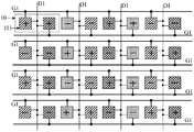
- FIG. 3 is a schematic structural diagram of an array substrate provided by an embodiment of the present disclosure.
- the array substrate may include: a plurality of data lines D1 (FIG. 3 only shows 4 data lines D1), and a plurality of gate lines G1 (FIG. 3 only shows 10 data lines D1), And a plurality of pixel units 10 arranged in an array ((only 16 pixel units 10 are shown in FIG. 3).
- Each pixel unit 10 may include one or more sub-pixels 101 located in the same row (each pixel unit 10 shown in FIG. 3 includes two sub-pixels 101).
- the sub-pixels 101 included in multiple pixel units 10 located in the same column may be connected to the same data line D1.
- two adjacent pixel units 10 may be connected to different gate lines G1.
- different sub-pixels 101 are connected to different gate lines G1.
- the polarity conversion directions of the data signals provided by two adjacent data lines D1 at the same time period are exactly the same.
- the pulling direction of Vcom is also the same, that is, it can be pulled up at the same time. Or pull down Vcom, thereby reducing the potential difference between the common electrode and the pixel electrode and improving the charging efficiency.
- each data line can provide a column of pixel units with a data signal whose polarity changes continuously, and two adjacent data lines can provide data signals with the same polarity at the same time. Since the gate lines connected to two adjacent pixel units in the same row are different, the two adjacent pixel units in the same row can be turned on at different times, so that two adjacent data lines can be connected to the same row and at different times. Two adjacent pixel units provide data signals, which can ensure that the polarities of the data signals provided to two adjacent pixel units in the same row are opposite, so that the polarities of the data signals loaded to any two adjacent pixel units are opposite.
- the potential of the common electrode can be pulled up or down at the same time, reducing the potential difference between the common electrode and the pixel electrode, and improving the charging efficiency .
- multiple pixel units 10 located in the same row may be connected to two gate line groups G0.
- the pixel unit 10 located in the odd-numbered column can be connected to one gate line group G0, and the pixel unit 10 located in the even-numbered column can be connected to another gate line group G0.
- the pixel units 10 in the first column and the third column in the first row of pixel units 10 shown in FIG. 3 are connected to the first gate line group G0; the pixel units 10 in the first row shown in FIG.
- the pixel units 10 in the second and fourth columns are connected to the second gate line group G0.
- each gate line group G0 may be the same as the number of sub-pixels 101 included in each pixel unit 10.
- each pixel 10 includes two sub-pixels 101, and correspondingly, each gate line group G0 shown in FIG. 3 includes two gate lines G1.
- the layout of the gate lines can be completed with less wiring space. That is, on the premise of improving the charging efficiency, the wiring process can be simplified, which is beneficial to realize a narrow frame, and can reduce the production cost of the array substrate.
- the pixel units 10 located in even-numbered columns in one row of pixel units 10 and the pixel units 10 located in odd-numbered columns in another row of pixel units 10 may be connected to each other. Connect to the same grid line group G0.
- the pixel units 10 located in the second and fourth columns in the first row of pixel units 10, and the pixel units 10 located in the first and third columns in the second row of pixel units 10 are respectively the same
- the second gate line group G0 is connected, that is, the second gate line group G0 is shared.
- the odd-numbered column and even-numbered column pixel units 10 of two adjacent rows of pixel units 10 share one gate line group G0, which can further save the array substrate.
- the wiring process is simplified and the production cost is reduced.
- the n-th sub-pixel 101 in each pixel unit 10 in the odd-numbered column may be connected to the n-th gate line G1 in one gate line group G0.
- the n-th sub-pixel 101 in each pixel unit 10 located in the even-numbered column may be connected to the n-th gate line G1 in another gate line group G0.
- n may be a positive integer not greater than N, and N may be the number of sub-pixels 101 included in each pixel unit 10.
- each pixel unit 10 includes two sub-pixels 101, that is, N is 2.
- N is 2.
- the first sub-pixel 101 in the pixel unit 10 in the first column and the first sub-pixel 101 in the pixel unit 10 in the third column are both the same as the first sub-pixel 101 in the pixel unit 10 in the third column.
- the first gate line G1 in the gate line group G0 is connected.
- the second sub-pixel 101 in the pixel unit 10 located in the first column and the second sub-pixel 101 in the pixel unit 10 located in the third column are both connected to the second gate line G1 in the first gate line group G0. connection.
- each pixel unit 10 may include a plurality of sub-pixels 101 of different colors.
- the colors of the sub-pixels 101 included in two adjacent pixel units 10 may be different.
- the colors of the two sub-pixels 101 included in the first pixel unit 10 located in the first row may be red and green; the colors of the two sub-pixels 101 included in the second pixel unit 10 located in the first row may be The colors of the sub-pixels 101 can be green and blue.
- the sub-pixels 101 included in the multiple pixel units 10 located in the same row may all be arranged cyclically in the order of the first-color sub-pixels, the second-color sub-pixels, and the third-color sub-pixels.
- the first color subpixel may be a red subpixel
- the second color subpixel may be a green subpixel
- the third color subpixel may be a blue subpixel.
- each pixel unit 10 may include two sub-pixels 101 of different colors.
- Each pixel unit 10 of the column may include two sub-pixels 101 of a red sub-pixel and a green sub-pixel.
- Each pixel unit 10 located in the second column may include two sub-pixels 101 of a blue sub-pixel and a red sub-pixel.
- Each pixel unit 10 located in the third column may include two sub-pixels 101 of a green sub-pixel and a blue sub-pixel.
- Each pixel unit 10 located in the fourth column may include two sub-pixels 101, a red sub-pixel and a green sub-pixel.
- each column of pixel unit 10 may include two columns of sub-pixels 101.
- each data line D1 may be located between two columns of sub-pixels 101 in a column of pixel units 10 to which it is connected. By arranging the data line D1 between the two columns of sub-pixels 101, it is advantageous to connect each column of sub-pixels 101 included in each column of pixel units 10 and the data line D1.
- each data line can provide a column of pixel units with a data signal whose polarity changes continuously, and two adjacent data lines can provide data signals with the same polarity at the same time. Since the gate lines connected to two adjacent pixel units in the same row are different, the two adjacent pixel units in the same row can be turned on at different times, so that two adjacent data lines can be connected to the same row and at different times. Two adjacent pixel units provide data signals, which can ensure that the polarities of the data signals provided to two adjacent pixel units in the same row are opposite, so that the polarities of the data signals loaded to any two adjacent pixel units are opposite.
- the potential of the common electrode can be pulled up or down at the same time, reducing the potential difference between the common electrode and the pixel electrode, and improving the charging efficiency .
- FIG. 4 is a flowchart of a driving method of an array substrate provided by an embodiment of the present disclosure, and the method can be applied to the array substrate shown in FIG. 3. As shown in Figure 4, the method may include:
- Step 401 sequentially providing gate driving signals to a plurality of gate lines included in the array substrate.
- the multiple gate lines included in the array substrate may all be connected to the gate driving circuit.
- the gate driving circuit may sequentially provide gate driving signals to the first row of gate lines to the last row of gate lines.
- Step 402 Provide each of the multiple data lines included in the array substrate with a data signal with a polarity conversion, wherein at the same time, the polarity of the data signal provided to two adjacent data lines is the same.
- a plurality of data lines included in the array substrate may all be connected to the source driving circuit.
- the source driving circuit can provide a data signal of continuously changing polarity to each data line, and at the same moment, the source driving circuit can provide data signals of the same polarity to two adjacent data lines.
- the embodiments of the present disclosure provide a method for driving an array substrate. Because this method can provide each data line included in the array substrate with a data signal of continuously changing polarity, and can provide data signals with the same polarity to two adjacent data lines at the same time. Therefore, in the array substrate, the gate lines connected to the sub-pixels in the same row and two adjacent pixel units are different, that is, when two adjacent data lines provide data signals to the same row and two adjacent pixel units at different times It can ensure that the polarities of the data signals provided to two adjacent pixel units in the same row are opposite, and meet the requirement that the polarities of the data signals loaded to any two adjacent pixel units are opposite.
- the potential of the common electrode can be pulled up or down at the same time, reducing the potential difference between the common electrode and the pixel electrode, and improving the charging efficiency .
- multiple pixel units 10 located in the same row may be connected to two gate line groups G0.
- the above step 402 may include:
- each data line is provided with a data signal of the first polarity; when the other gate line group G0 in the two gate line groups is provided.
- a data signal of the second polarity is provided to each data line.
- the first polarity may be positive polarity
- the second polarity may be negative polarity.
- FIG. 5 is an equivalent circuit diagram of a sub-pixel provided in an embodiment of the present disclosure.
- each sub-pixel may include a thin film transistor T1 and a liquid crystal capacitor CLC.
- the liquid crystal capacitor CLC may be a capacitor formed by the pixel electrode PI and the common electrode COM.
- the gate of the thin film transistor T1 can be connected to the gate line G1, the first electrode can be connected to the data line D1, and the second electrode can be connected to one end of the liquid crystal capacitor CLC.
- the gate line G1 provides a gate driving signal to the thin film transistor T1
- the data line D1 can transmit the data signal to the pixel electrode PI through the thin film transistor T1, so as to charge the pixel electrode PI.
- Fig. 6 is a signal timing diagram provided by an embodiment of the present disclosure. Taking the first column of pixel units and the second column of pixel units in the array substrate shown in FIG. 3, and the circuit structure of the sub-pixel 101 as the structure shown in FIG. 5 as an example, the driving principle of the array substrate provided by the embodiment of the present disclosure is introduced. .
- the gate lines G1 connected to two adjacent pixel units 10 in the same row are different, and the gate lines G1 connected to the sub-pixels 101 included in each pixel unit 10 are also different. Therefore, when the gate driving signals are sequentially provided to the two gate lines G1 included in the first gate line group G0 connected to the first row of pixel units 10, the two sub The thin film transistors T1 in the pixels 101 are sequentially turned on.
- the first data line D1 may sequentially provide positive polarity data signals to two sub-pixels 101 included in the pixel unit 10 located in the first row and the first row of the first column.
- the gate driving signals are successively provided to the two gate lines G1 included in the second gate line group G0 connected to the first row of pixel units 10, the two sub-pixels included in the pixel unit 10 located in the second row of the first column
- the thin film transistors T1 in 101 are sequentially turned on.
- the thin film transistors T1 in the two sub-pixels 101 included in the pixel unit 10 in the first row of the second column are also turned on sequentially.
- the second data line D1 may also be used to The two sub-pixels 101 included in the pixel unit 10 located in the first row of the second column sequentially provide data signals of negative polarity.
- the driving sequence after the second row can be deduced by analogy.
- Vcom can be pulled down when the polarity of the data signal is switched from positive to negative, correspondingly, Vcom can be pulled high when the polarity of the data signal is switched from negative to positive. Therefore, referring to FIG. 6, when the polarities of the data signals provided by the first data line D1 and the second data line D1 in the same time period are changed from positive polarity to negative polarity at the same time, the downward fluctuation of Vcom can be caused ( That is, ripple). When the polarities of the data signals provided by the first data line D1 and the second data line D1 in the same time period are changed from negative polarity to positive polarity at the same time, the Vcom can generate upward ripple.
- V Vp-Vcom. Therefore, whether it is pulling down or pulling up Vcom, the potential difference between the pixel electrode and the common electrode can be reduced, and the charging efficiency can be improved.
- the common electrode since the common electrode has a voltage-stabilizing ability, referring to FIG. 6, the upward and downward ripples appearing on Vcom will gradually return to the potential before the ripple is generated, so that the pixel electrode can be charged normally.
- the potential Vcom of the common electrode when the potential Vcom of the common electrode is pulled down, the potential of the pixel electrode can be simultaneously pulled down through the coupling effect of the coupling capacitor; when the potential Vcom of the common electrode is pulled down When pulled high, the potential of the pixel electrode can be simultaneously pulled high through the coupling effect of the coupling capacitor, so that the potential of the pixel electrode can accurately reach the target potential, that is, the potential that needs to be written to the liquid crystal molecules, which reduces the source to a certain extent. Power consumption of the drive circuit.
- FIG. 7 is a signal timing diagram in another array substrate provided by an embodiment of the present disclosure. Take driving the first sub-pixel 101 in the pixel unit 10 in the first column and second row in the array substrate shown in FIG. 3, and take the circuit structure of the sub-pixel 101 as the structure shown in FIG. 5 as an example, The driving principle of the sub-pixel 101 is introduced. 3, it can be seen that the first sub-pixel 101 located in the second row of the first column is connected to the first gate line G1 in the second gate line group G0, and is connected to the first data line D1.
- the first gate line G1 in the second gate line group G0 provides a gate driving signal, and the thin film transistor T1 in the first sub-pixel 101 in the first column and second row is turned on.
- the first data line D1 provides a data signal of negative polarity to the sub-pixel 101. It can be seen from FIG. 7 that in the stage T0 before the stage T1, the polarity of the data signal provided by the first data line D1 is positive. Therefore, when transitioning from stage T0 to stage T1, the data signal provided by the first data line D1 changes from positive polarity to negative polarity. Accordingly, referring to FIG.
- the potential Vcom of the common electrode can be Produce a downward ripple.
- the potential Vp of the pixel electrode is also pulled down under the coupling action of the coupling capacitor.
- the potential Vcom of the common electrode is gradually restored to the potential before the ripple is generated under the effect of the voltage stabilizing ability of the common electrode.
- the potential Vp of the pixel electrode is further pulled down, charging the liquid crystal molecules in the first sub-pixel 101 in the first column and second row. Therefore, this phase T1 can also be referred to as the charging phase.
- the first gate line G1 in the second gate line group G0 stops providing gate driving signals, and the thin film transistor T1 in the first sub-pixel 101 in the first column and second row is turned off.
- the liquid crystal molecules in the first sub-pixel 101 can be deflected to a target angle, and accordingly, the first sub-pixel 101 starts to emit light. Therefore, this stage T2 can also be referred to as the display stage.
- the embodiments of the present disclosure provide a method for driving an array substrate. Because this method can provide each data line included in the array substrate with a data signal of continuously changing polarity, and can provide data signals with the same polarity to two adjacent data lines at the same time. Therefore, in the array substrate, the gate lines connected to the sub-pixels in the same row and two adjacent pixel units are different, that is, when two adjacent data lines provide data signals to the same row and two adjacent pixel units at different times It can ensure that the polarities of the data signals provided to two adjacent pixel units in the same row are opposite, and meet the requirement that the polarities of the data signals loaded to any two adjacent pixel units are opposite.
- the potential of the common electrode can be pulled up or down at the same time, reducing the potential difference between the common electrode and the pixel electrode, and improving the charging efficiency .
- the embodiment of the present disclosure also provides a display device, which may include: an array substrate as shown in FIG. 3 and a driving circuit connected to the array substrate.
- the driving circuit may include: a source driving circuit and a gate driving circuit.
- the gate driving circuit can be connected to a plurality of gate lines in the array substrate, and the source driving circuit can be connected to a plurality of data lines in the array substrate.
- the gate driving circuit is used to provide gate driving signals to a plurality of gate lines, and the source driving circuit is used to provide data signals to a plurality of data lines.
- the display device may be any product or component with a display function such as a liquid crystal panel, electronic paper, mobile phone, tablet computer, television, monitor, notebook computer, digital photo frame, etc.
- the display device may include several rows and several columns of sub-pixels Px in the display area.
- the gate driving circuit 21 is connected to a plurality of gate lines G1 to provide gate driving signals to the plurality of gate lines;
- the source driving circuit 22 is connected to a plurality of data lines D1 to provide Provide data signals. 3 it can be seen that the intersection of multiple data lines D1 and multiple gate lines G1 defines multiple sub-pixels Px in the array substrate; in one example, multiple sub-pixels Px are all located in the active display area (Active Area) of the display device. ), and the gate drive circuit 21 and the source drive circuit 22 are outside the effective display area.
- non-transitory computer-readable storage medium including instructions, such as a memory including instructions, which can be executed by a processor of a computer to complete the driving methods shown in each embodiment of the present disclosure .
- the non-transitory computer-readable storage medium may be ROM, random access memory (RAM), CD-ROM, magnetic tape, floppy disk, optical data storage device, etc.
Landscapes
- Physics & Mathematics (AREA)
- Engineering & Computer Science (AREA)
- General Physics & Mathematics (AREA)
- Chemical & Material Sciences (AREA)
- Crystallography & Structural Chemistry (AREA)
- Nonlinear Science (AREA)
- Computer Hardware Design (AREA)
- Theoretical Computer Science (AREA)
- Mathematical Physics (AREA)
- Optics & Photonics (AREA)
- Microelectronics & Electronic Packaging (AREA)
- Control Of Indicators Other Than Cathode Ray Tubes (AREA)
- Liquid Crystal Display Device Control (AREA)
- Liquid Crystal (AREA)
Abstract
Description
本申请要求于2019年5月22日提交的、申请号为201910429469.X、发明名称为“阵列基板及其驱动方法、显示装置”的中国专利申请的优先权,其全部内容通过引用结合在本申请中。This application claims the priority of the Chinese patent application filed on May 22, 2019 with the application number 201910429469.X and the invention title "Array substrate and its driving method, display device", the entire content of which is incorporated herein by reference Applying.
本公开涉及显示技术领域,特别涉及一种阵列基板及其驱动方法、显示装置。The present disclosure relates to the field of display technology, and in particular to an array substrate, a driving method thereof, and a display device.
液晶显示(liquid crystal display,LCD)装置因其分辨率高、重量轻和低能耗等优点被广泛应用于显示领域中。Liquid crystal display (LCD) devices are widely used in the display field due to their advantages of high resolution, light weight, and low energy consumption.
液晶显示装置中的每个子像素可以包括薄膜晶体管、像素电极、公共电极以及液晶分子。其中,薄膜晶体管可以与数据线和像素电极连接,数据线可以通过薄膜晶体管将数据信号加载至像素电极,使得液晶分子在像素电极和公共电极间电位差作用下发生偏转。但是,若长时间向像素电极加载相同极性的数据信号,液晶分子可能会出现极化现象,即出现偏转速度较慢,偏转幅度较小的现象。Each sub-pixel in the liquid crystal display device may include a thin film transistor, a pixel electrode, a common electrode, and liquid crystal molecules. Among them, the thin film transistor can be connected to the data line and the pixel electrode, and the data line can load the data signal to the pixel electrode through the thin film transistor, so that the liquid crystal molecules are deflected under the action of the potential difference between the pixel electrode and the common electrode. However, if data signals of the same polarity are applied to the pixel electrodes for a long time, the liquid crystal molecules may be polarized, that is, the deflection speed is slower and the deflection amplitude is smaller.
发明内容Summary of the invention
本公开提供了一种阵列基板及其驱动方法、显示装置、The present disclosure provides an array substrate and a driving method thereof, a display device,
一方面,提供了一种阵列基板,所述阵列基板包括:多条数据线,多条栅线,以及阵列排布的多个像素单元,每个像素单元包括位于同一行的一个或多个子像素;In one aspect, an array substrate is provided. The array substrate includes a plurality of data lines, a plurality of gate lines, and a plurality of pixel units arranged in an array. Each pixel unit includes one or more sub-pixels located in the same row. ;
位于同一列的多个像素单元所包括的子像素与同一条所述数据线连接;The sub-pixels included in multiple pixel units located in the same column are connected to the same data line;
位于同一行的多个像素单元中,相邻两个像素单元与不同的栅线连接,且每个像素单元中,不同子像素所连接的栅线不同。Among the multiple pixel units located in the same row, two adjacent pixel units are connected to different gate lines, and in each pixel unit, different sub-pixels are connected to different gate lines.
可选的,位于同一行的多个像素单元与两个栅线组连接,且位于同一行的多 个像素单元中,位于奇数列的像素单元与一个所述栅线组连接,位于偶数列的像素单元与另一个所述栅线组连接;Optionally, multiple pixel units located in the same row are connected to two gate line groups, and among multiple pixel units located in the same row, the pixel units located in odd-numbered columns are connected to one of the gate line groups, which are located in even-numbered columns. The pixel unit is connected to another gate line group;
其中,每个栅线组包括的栅线的条数,与每个像素单元包括的子像素的个数相同。Wherein, the number of gate lines included in each gate line group is the same as the number of sub-pixels included in each pixel unit.
可选的,相邻两行像素单元中,一行像素单元中位于偶数列的像素单元,与另一行像素单元中位于奇数列的像素单元分别与同一个所述栅线组连接。Optionally, in two adjacent rows of pixel units, pixel units located in even columns in one row of pixel units and pixel units located in odd columns in another row of pixel units are respectively connected to the same gate line group.
可选的,位于奇数列的每个像素单元中的第n个子像素均与一个所述栅线组中的第n条栅线连接,位于偶数列的每个像素单元中的第n个子像素均与另一个所述栅线组中的第n条栅线连接;Optionally, the n-th sub-pixel in each pixel unit in the odd-numbered column is connected to the n-th gate line in the gate line group, and the n-th sub-pixel in each pixel unit in the even-numbered column is connected Connected to the nth gate line in the other gate line group;
其中,n为不大于N的正整数,N为每个像素单元包括的子像素的个数。Wherein, n is a positive integer not greater than N, and N is the number of sub-pixels included in each pixel unit.
可选的,每个所述像素单元包括多个不同颜色的子像素。Optionally, each pixel unit includes multiple sub-pixels of different colors.
可选的,位于同一行的多个像素单元包括的子像素按照第一颜色子像素、第二颜色子像素和第三颜色子像素的顺序依次循环排布。Optionally, the sub-pixels included in the multiple pixel units located in the same row are arranged in a cycle in sequence in the order of the first-color sub-pixels, the second-color sub-pixels, and the third-color sub-pixels.
可选的,所述第一颜色子像素为红色子像素,所述第二颜色子像素为绿色子像素,所述第三颜色子像素为蓝色子像素。Optionally, the first color subpixel is a red subpixel, the second color subpixel is a green subpixel, and the third color subpixel is a blue subpixel.
可选的,每个所述像素单元包括两个不同颜色的子像素。Optionally, each pixel unit includes two sub-pixels of different colors.
可选的,每条所述数据线均位于其所连接的一列像素单元中的两列子像素之间。Optionally, each data line is located between two columns of sub-pixels in a column of pixel units connected to it.
另一方面,提供了一种阵列基板的驱动方法,应用于如上述方面所述的阵列基板中,所述方法包括:In another aspect, a method for driving an array substrate is provided, which is applied to the array substrate as described in the above aspect, and the method includes:
向所述阵列基板包括的多条栅线依次提供栅极驱动信号;Sequentially providing gate driving signals to a plurality of gate lines included in the array substrate;
向所述阵列基板包括的多条数据线中的每条数据线提供极性变换的数据信号,其中,在同一时刻,向相邻两条数据线提供的数据信号的极性相同。Each of the plurality of data lines included in the array substrate is provided with a data signal with a polarity changed, wherein at the same time, the data signals provided to two adjacent data lines have the same polarity.
可选的,位于同一行的多个像素单元与两个栅线组连接;所述向所述阵列基板包括的多条数据线中的每条数据线提供极性变换的数据信号,包括:Optionally, a plurality of pixel units located in the same row are connected to two gate line groups; the providing each of the plurality of data lines included in the array substrate with a data signal of polarity conversion includes:
在向所述两个栅线组中的一个栅线组提供栅极驱动信号时,向每条所述数据线提供第一极性的数据信号;When providing a gate driving signal to one of the two gate line groups, providing a data signal of the first polarity to each of the data lines;
在向所述两个栅线组中的另一个栅线组提供栅极驱动信号时,向每条所述数据线提供第二极性的数据信号。When a gate driving signal is provided to the other of the two gate line groups, a data signal of the second polarity is provided to each of the data lines.
又一方面,提供了一种显示装置,所述显示装置包括:如上述方面所述的阵列基板,以及与所述阵列基板连接的驱动电路。In yet another aspect, a display device is provided, the display device comprising: the array substrate as described in the above aspect, and a driving circuit connected to the array substrate.
可选的,所述驱动电路包括:源极驱动电路和栅极驱动电路;Optionally, the driving circuit includes: a source driving circuit and a gate driving circuit;
所述栅极驱动电路与所述阵列基板中的多条栅线连接,所述源极驱动电路与所述阵列基板中的多条数据线连接;The gate driving circuit is connected to a plurality of gate lines in the array substrate, and the source driving circuit is connected to a plurality of data lines in the array substrate;
所述栅极驱动电路用于向所述多条栅线提供栅极驱动信号;The gate driving circuit is used to provide gate driving signals to the plurality of gate lines;
所述源极驱动电路用于向所述多条数据线提供数据信号。The source driving circuit is used to provide data signals to the plurality of data lines.
为了更清楚地说明本公开实施例中的技术方案,下面将对实施例描述中所需要使用的附图作简单地介绍,显而易见地,下面描述中的附图仅仅是本公开的一些实施例,对于本领域普通技术人员来讲,在不付出创造性劳动的前提下,还可以根据这些附图获得其他的附图。In order to more clearly describe the technical solutions in the embodiments of the present disclosure, the following will briefly introduce the accompanying drawings used in the description of the embodiments. Obviously, the accompanying drawings in the following description are only some embodiments of the present disclosure. For those of ordinary skill in the art, other drawings can be obtained from these drawings without creative work.
图1是本公开实施例提供的一种阵列基板的结构示意图;FIG. 1 is a schematic structural diagram of an array substrate provided by an embodiment of the present disclosure;
图2是本公开实施例提供的一种阵列基板中各信号端的时序图;2 is a timing diagram of each signal terminal in an array substrate provided by an embodiment of the present disclosure;
图3是本公开实施例提供的另一种阵列基板的结构示意图;FIG. 3 is a schematic structural diagram of another array substrate provided by an embodiment of the present disclosure;
图4是本公开实施例提供的一种阵列基板的驱动方法流程图;4 is a flowchart of a driving method of an array substrate provided by an embodiment of the present disclosure;
图5是本公开实施例提供的一种子像素的等效电路图;FIG. 5 is an equivalent circuit diagram of a sub-pixel provided by an embodiment of the present disclosure;
图6是本公开实施例提供的另一种阵列基板中各信号端的时序图;6 is a timing diagram of each signal terminal in another array substrate provided by an embodiment of the present disclosure;
图7是本公开实施例提供的又一种阵列基板中各信号端的时序图;FIG. 7 is a timing diagram of each signal terminal in another array substrate provided by an embodiment of the present disclosure;
图8和图9是本公开实施例提供的一种显示装置的结构示意图。8 and 9 are schematic diagrams of the structure of a display device provided by embodiments of the present disclosure.
为了使本公开的目的、技术方案和优点更加清楚,下面将结合附图对本公开实施方式作进一步地详细描述。In order to make the objectives, technical solutions, and advantages of the present disclosure clearer, the following further describes the embodiments of the present disclosure in detail with reference to the accompanying drawings.
相关技术中,为了避免液晶分子出现极化现象,可以控制加载至像素电极的数据信号在正极性和负极性之间不断切换(称为极性反转)。但是,由于公共电极和数据线之间存在耦合电容,因此当加载至像素电极的数据信号的极性发生变化时,公共电极在耦合电容的作用下也发生相应的变化,导致公共电极和像素电极间电位差较大,数据线为像素电极进行充电的充电效率较低。In the related art, in order to avoid the polarization phenomenon of the liquid crystal molecules, the data signal loaded to the pixel electrode can be controlled to switch between the positive polarity and the negative polarity (called polarity inversion). However, due to the coupling capacitor between the common electrode and the data line, when the polarity of the data signal loaded to the pixel electrode changes, the common electrode also changes correspondingly under the action of the coupling capacitor, resulting in the common electrode and the pixel electrode. The potential difference between the data lines is large, and the charging efficiency of the data line for charging the pixel electrode is low.
其中,极性反转的方式可以包括帧反转、列反转、行反转和点(dot)反转等。点反转可以包括2dot反转和1+2dot反转。2dot反转是指加载至每个像素单元包括的每个子像素的数据信号的极性相同,且加载至相邻两个像素单元的 数据信号的极性相反。1+2dot反转是指加载至相邻两个像素单元中相邻两个子像素的数据信号的极性相同,且加载至每个像素单元包括的每个子像素的数据信号的极性相反,每个像素单元包括2个子像素。Among them, the manner of polarity inversion may include frame inversion, column inversion, row inversion, dot inversion, and so on. Dot inversion can include 2dot inversion and 1+2dot inversion. 2dot inversion means that the polarity of the data signal loaded to each sub-pixel included in each pixel unit is the same, and the polarity of the data signal loaded to two adjacent pixel units is opposite. 1+2dot inversion means that the polarity of the data signal loaded to two adjacent sub-pixels in two adjacent pixel units is the same, and the polarity of the data signal loaded to each sub-pixel included in each pixel unit is opposite. Each pixel unit includes 2 sub-pixels.
为了便于理解,这里提供一种2dot反转的实现方式作为后文的参照。图1是本公开实施例提供的一种显示基板的结构示意图。图1以显示基板包括8条栅线G1,4条数据线D1,16个像素单元10,以及每个像素单元10包括2个子像素101为例进行说明。参考图1,每条数据线D1向每个像素单元10包括的两个子像素101提供的数据信号的极性相同,相邻两条数据线D1向位于同一行的两个像素单元10提供的数据信号的极性相反,每条数据线D1向位于同一列且相邻的两个像素单元10提供的数据信号的极性相反,满足2dot反转。For ease of understanding, here is an implementation of 2dot inversion as a reference for the following text. FIG. 1 is a schematic structural diagram of a display substrate provided by an embodiment of the present disclosure. FIG. 1 illustrates an example in which the display substrate includes 8 gate lines G1, 4 data lines D1, 16
但是,由于图1所示的阵列基板中,位于同一行且相邻的两个像素单元10中的子像素101连接的栅线G1相同,因此,该两个像素单元10中与同一条栅线G1连接的子像素101会同时开启,本公开实施例描述的子像素开启均是指子像素包括的薄膜晶体管开启(工作在线性区或饱和区)。相应的,相邻两条数据线D1可以同时向相邻两个像素单元10提供数据信号。However, since in the array substrate shown in FIG. 1, the gate lines G1 connected to the sub-pixels 101 in the same row and adjacent two
又由于相邻两条数据线D1向位于同一行的两个像素单元10提供的数据信号的极性相反,因此相邻两条数据线D1在同一时间段提供的数据信号的极性变换方向正好相反。由于数据线D1和公共电极之间还存在耦合电容,在耦合电容的耦合作用下,当数据信号由正极性变换至负极性时可以拉低公共电极的电位Vcom,当数据信号由负极性切换至正极性时可以拉高Vcom。因此当相邻两条数据线D1在同一时间段提供的数据信号的极性变换方向正好相反时,对Vcom拉动方向也正好相反,Vcom大体上不变。In addition, since the polarities of the data signals provided by the two adjacent data lines D1 to the two
例如,以图1所示的第一列和第二列像素单元10为例。参考图2,在第一条数据线D1向位于第一列第一行的像素单元10依次写入正极性的数据信号时,第二条数据线D1也同时向位于第二列第一行的像素单元10依次写入负极性的数据信号。在第一条数据线D1向位于第一列第二行的像素单元10依次写入负极性的数据信号时,第二条数据线D1也同时向位于第二列第二行的像素单元10依次写入正极性的数据信号。且参考图2,Vcom在极性变换的拉动作用下保持恒定。For example, take the first column and the second column of
图3是本公开实施例提供的一种阵列基板的结构示意图。如图3所示,该阵列基板可以包括:多条数据线D1(图3仅示出了4条数据线D1),多条栅线G1(图3仅示出了10条数据线D1),以及阵列排布的多个像素单元10((图3仅示出了16个像素单元10)。FIG. 3 is a schematic structural diagram of an array substrate provided by an embodiment of the present disclosure. As shown in FIG. 3, the array substrate may include: a plurality of data lines D1 (FIG. 3 only shows 4 data lines D1), and a plurality of gate lines G1 (FIG. 3 only shows 10 data lines D1), And a plurality of
每个像素单元10可以包括位于同一行的一个或多个子像素101(图3示出的每个像素单元10包括两个子像素101)。位于同一列的多个像素单元10所包括的子像素101可以与同一条数据线D1连接。并且,位于同一行的多个像素单元10中,相邻两个像素单元10可以与不同的栅线G1连接,每个像素单元10中,不同子像素101所连接的栅线G1不同。Each
当多条栅线G1依次提供栅极驱动信号时,相对于图1所示的阵列基板,通过使位于同一行且相邻两个像素单元10与不同的栅线G1连接,且使每个像素单元10包括的不同子像素101与不同的栅线G1连接,可以保证位于同一行且相邻的两个像素单元10包括的子像素101能够不同时开启,进而可以使得相邻两条数据线D1在不同时刻向位于同一行且相邻的两个像素单元10提供数据信号,进而可以使得加载至任意两个相邻像素单元10的数据信号的极性相反,满足极性反转的要求。在采用2dot方式驱动时,相邻两条数据线D1在同一时间段提供的数据信号的极性变换方向即正好相同,相应的,对Vcom的拉动方向也相同,也即是,可以同时拉高或拉低Vcom,从而可以减小公共电极和像素电极间的电位差,提高充电效率。When multiple gate lines G1 sequentially provide gate driving signals, with respect to the array substrate shown in FIG. 1, two
综上所述,本公开实施例提供了一种阵列基板。该阵列基板在驱动时,可以使得每条数据线向一列像素单元提供极性不断变换的数据信号,且使得相邻两条数据线在同一时刻提供极性相同的数据信号。由于位于同一行且相邻的两个像素单元连接的栅线不同,因此可以使得同一行且相邻两个像素单元不同时开启,进而使得相邻两条数据线可以在不同时刻向同一行且相邻的两个像素单元提供数据信号,可以确保向同一行且相邻的两个像素单元提供的数据信号的极性相反,满足加载至任意两个相邻像素单元的数据信号的极性相反,避免液晶分子出现极化现象的要求。并且,由于相邻数据线在同一时间段提供的数据信号的极性变换方向相同,因此可以同时拉高或拉低公共电极的电位,减小公共电极和像素电极间的电位差,提高充电效率。In summary, the embodiments of the present disclosure provide an array substrate. When the array substrate is driven, each data line can provide a column of pixel units with a data signal whose polarity changes continuously, and two adjacent data lines can provide data signals with the same polarity at the same time. Since the gate lines connected to two adjacent pixel units in the same row are different, the two adjacent pixel units in the same row can be turned on at different times, so that two adjacent data lines can be connected to the same row and at different times. Two adjacent pixel units provide data signals, which can ensure that the polarities of the data signals provided to two adjacent pixel units in the same row are opposite, so that the polarities of the data signals loaded to any two adjacent pixel units are opposite. , To avoid the requirement of polarization phenomenon of liquid crystal molecules. In addition, since the data signals provided by adjacent data lines in the same time period have the same polarity conversion direction, the potential of the common electrode can be pulled up or down at the same time, reducing the potential difference between the common electrode and the pixel electrode, and improving the charging efficiency .
可选的,参考图3,位于同一行的多个像素单元10可以与两个栅线组G0 连接。并且,位于同一行的多个像素单元10中,位于奇数列的像素单元10可以与一个栅线组G0连接,位于偶数列的像素单元10可以与另一个栅线组G0连接。Optionally, referring to FIG. 3,
例如,如图3所示的第一行像素单元10中位于第一列和第三列的像素单元10与第一个栅线组G0连接;图3所示的第一行像素单元10中位于第二列和第四列的像素单元10与第二个栅线组G0连接。For example, the
在本公开实施例中,每个栅线组G0包括的栅线G1的条数,与每个像素单元10包括的子像素101的个数可以相同。例如,参考图3,每个像素10包括两个子像素101,相应的,图3示出的每个栅线组G0即包括2条栅线G1。In the embodiment of the present disclosure, the number of gate lines G1 included in each gate line group G0 may be the same as the number of
通过仅设置两个栅线组G0与同一行像素单元10连接,仅需较少的布线空间即可完成对栅线的布置。也即是,可以在提高充电效率的前提下,简化布线工艺,有利于实现窄边框,且可以降低阵列基板的生产成本。By setting only two gate line groups G0 to be connected to the same row of
可选的,在本公开实施例中,相邻两行像素单元10中,一行像素单元10中位于偶数列的像素单元10,与另一行像素单元10中位于奇数列的像素单元10可以分别与同一个栅线组G0连接。Optionally, in the embodiment of the present disclosure, in two adjacent rows of
例如,参考图3,第一行像素单元10中位于第二列和第四列的像素单元10,以及第二行像素单元10中位于第一列和第三列的像素单元10分别与同一个第二个栅线组G0连接,即共用第二个栅线组G0。For example, referring to FIG. 3, the
通过在设置同一行像素单元10与两个栅线组G0连接的前提下,再将相邻两行像素单元10的奇数列和偶数列像素单元10共用一个栅线组G0,可以进一步节省阵列基板中的布线空间,简化布线工艺,降低生产成本。Under the premise that the
可选的,位于奇数列的每个像素单元10中的第n个子像素101均可以与一个栅线组G0中的第n条栅线G1连接。位于偶数列的每个像素单元10中的第n个子像素101均可以与另一个栅线组G0中的第n条栅线G1连接。其中,n可以为不大于N的正整数,N可以为每个像素单元10包括的子像素101的个数。通过设置每个像素单元10中的第n个子像素101与每个栅线组中的第n条栅线连接,有利于栅线G1的排布。Optionally, the n-
例如,参考图3,每个像素单元10包括两个子像素101,也即是N为2。以第一行像素单元10为例,位于第一列的像素单元10中的第一个子像素101,与位于第三列的像素单元10中的第一个子像素101,均与第一个栅线组G0中的第一条栅线G1连接。位于第一列的像素单元10中的第二个子像素101,与 位于第三列的像素单元10中的第二个子像素101,均与第一个栅线组G0中的第二条栅线G1连接。For example, referring to FIG. 3, each
在本公开实施例中,每个像素单元10可以包括多个不同颜色的子像素101。并且,相邻的两个像素单元10包括的子像素101的颜色可以不同。In the embodiment of the present disclosure, each
例如,对于图3所示的阵列基板,位于第一行的第一个像素单元10包括的两个子像素101的颜色可以为红色和绿色;位于第一行的第二个像素单元10包括的两个子像素101的颜色可以为绿色和蓝色。For example, for the array substrate shown in FIG. 3, the colors of the two sub-pixels 101 included in the
可选的,位于同一行的多个像素单元10包括的子像素101均可以按照第一颜色子像素、第二颜色子像素和第三颜色子像素的顺序依次循环排布。其中,该第一颜色子像素可以为红色子像素,该第二颜色子像素可以为绿色子像素,该第三颜色子像素可以为蓝色子像素。Optionally, the sub-pixels 101 included in the
可选的,每个像素单元10可以包括两个不同颜色的子像素101。当位于同一行的多个像素单元10包括的子像素101按照红色子像素、绿色子像素和蓝色子像素顺序依次循环排布时,相应的,对于图3所示的阵列基板,位于第一列的每个像素单元10即可以包括红色子像素和绿色子像素两个子像素101。位于第二列的每个像素单元10即可以包括蓝色子像素和红色子像素两个子像素101。位于第三列的每个像素单元10即可以包括绿色子像素和蓝色子像素两个子像素101。位于第四列的每个像素单元10即可以包括红色子像素和绿色子像素两个子像素101。Optionally, each
可选的,参考图3,当每个像素单元10包括两个子像素101时,每列像素单元10即可以包括两列子像素101。相应的,参考图3,每条数据线D1可以均位于其所连接的一列像素单元10中的两列子像素101之间。通过将数据线D1设置在两列子像素101之间,有利于每列像素单元10包括的每列子像素101与数据线D1的连接。Optionally, referring to FIG. 3, when each
综上所述,本公开实施例提供了一种阵列基板。该阵列基板在驱动时,可以使得每条数据线向一列像素单元提供极性不断变换的数据信号,且使得相邻两条数据线在同一时刻提供极性相同的数据信号。由于位于同一行且相邻的两个像素单元连接的栅线不同,因此可以使得同一行且相邻两个像素单元不同时开启,进而使得相邻两条数据线可以在不同时刻向同一行且相邻的两个像素单元提供数据信号,可以确保向同一行且相邻的两个像素单元提供的数据信号的极性相反,满足加载至任意两个相邻像素单元的数据信号的极性相反,避免 液晶分子出现极化现象的要求。并且,由于相邻数据线在同一时间段提供的数据信号的极性变换方向相同,因此可以同时拉高或拉低公共电极的电位,减小公共电极和像素电极间的电位差,提高充电效率。In summary, the embodiments of the present disclosure provide an array substrate. When the array substrate is driven, each data line can provide a column of pixel units with a data signal whose polarity changes continuously, and two adjacent data lines can provide data signals with the same polarity at the same time. Since the gate lines connected to two adjacent pixel units in the same row are different, the two adjacent pixel units in the same row can be turned on at different times, so that two adjacent data lines can be connected to the same row and at different times. Two adjacent pixel units provide data signals, which can ensure that the polarities of the data signals provided to two adjacent pixel units in the same row are opposite, so that the polarities of the data signals loaded to any two adjacent pixel units are opposite. , To avoid the requirement of polarization phenomenon of liquid crystal molecules. In addition, since the data signals provided by adjacent data lines in the same time period have the same polarity conversion direction, the potential of the common electrode can be pulled up or down at the same time, reducing the potential difference between the common electrode and the pixel electrode, and improving the charging efficiency .
图4是本公开实施例提供的一种阵列基板的驱动方法的流程图,该方法可以应用于如图3所示的阵列基板中。如图4所示,该方法可以包括:FIG. 4 is a flowchart of a driving method of an array substrate provided by an embodiment of the present disclosure, and the method can be applied to the array substrate shown in FIG. 3. As shown in Figure 4, the method may include:
步骤401、向阵列基板包括的多条栅线依次提供栅极驱动信号。Step 401: sequentially providing gate driving signals to a plurality of gate lines included in the array substrate.
在本公开实施例中,阵列基板包括的多条栅线可以均与栅极驱动电路连接。栅极驱动电路可以向第一行栅线到最后一行栅线依次提供栅极驱动信号。In the embodiment of the present disclosure, the multiple gate lines included in the array substrate may all be connected to the gate driving circuit. The gate driving circuit may sequentially provide gate driving signals to the first row of gate lines to the last row of gate lines.
步骤402、向阵列基板包括的多条数据线中的每条数据线提供极性变换的数据信,其中,在同一时刻,向相邻两条数据线提供的数据信号的极性相同。Step 402: Provide each of the multiple data lines included in the array substrate with a data signal with a polarity conversion, wherein at the same time, the polarity of the data signal provided to two adjacent data lines is the same.
在本公开实施例中,阵列基板包括的多条数据线可以均与源极驱动电路连接。源极驱动电路可以向每条数据线提供极性不断变换的数据信号,且在同一时刻,源极驱动电路可以向相邻两条数据线提供极性相同的数据信号。In the embodiment of the present disclosure, a plurality of data lines included in the array substrate may all be connected to the source driving circuit. The source driving circuit can provide a data signal of continuously changing polarity to each data line, and at the same moment, the source driving circuit can provide data signals of the same polarity to two adjacent data lines.
综上所述,本公开实施例提供了一种阵列基板的驱动方法。由于该方法可以向阵列基板包括的每条数据线提供极性不断变换的数据信号,且可以在同一时刻向相邻两条数据线提供极性相同的数据信号。因此在阵列基板中位于同一行且相邻两个像素单元包括的子像素连接的栅线不同,即相邻两条数据线在不同时刻向同一行且相邻的两个像素单元提供数据信号时,可以确保向同一行且相邻的两个像素单元提供的数据信号的极性相反,满足加载至任意两个相邻像素单元的数据信号的极性相反的要求。并且,由于相邻数据线在同一时间段提供的数据信号的极性变换方向相同,因此可以同时拉高或拉低公共电极的电位,减小公共电极和像素电极间的电位差,提高充电效率。In summary, the embodiments of the present disclosure provide a method for driving an array substrate. Because this method can provide each data line included in the array substrate with a data signal of continuously changing polarity, and can provide data signals with the same polarity to two adjacent data lines at the same time. Therefore, in the array substrate, the gate lines connected to the sub-pixels in the same row and two adjacent pixel units are different, that is, when two adjacent data lines provide data signals to the same row and two adjacent pixel units at different times It can ensure that the polarities of the data signals provided to two adjacent pixel units in the same row are opposite, and meet the requirement that the polarities of the data signals loaded to any two adjacent pixel units are opposite. In addition, since the data signals provided by adjacent data lines in the same time period have the same polarity conversion direction, the potential of the common electrode can be pulled up or down at the same time, reducing the potential difference between the common electrode and the pixel electrode, and improving the charging efficiency .
可选的,参考图3,在本公开实施例中,位于同一行的多个像素单元10可以与两个栅线组G0连接。相应的,上述步骤402即可以包括:Optionally, referring to FIG. 3, in the embodiment of the present disclosure,
在向两个栅线组中的一个栅线组G0提供栅极驱动信号时,向每条数据线提供第一极性的数据信号;在向两个栅线组中的另一个栅线组G0提供栅极驱动信号时,向每条数据线提供第二极性的数据信号。该第一极性可以为正极性,该第二极性可以为负极性。When a gate drive signal is provided to one gate line group G0 in the two gate line groups, each data line is provided with a data signal of the first polarity; when the other gate line group G0 in the two gate line groups is provided When the gate driving signal is provided, a data signal of the second polarity is provided to each data line. The first polarity may be positive polarity, and the second polarity may be negative polarity.
可选的,图5是本公开实施例提供的一种子像素的等效电路图。如图5所示,每个子像素可以包括:薄膜晶体管T1和液晶电容CLC,液晶电容CLC 可以是由像素电极PI和公共电极COM形成的电容。薄膜晶体管T1的栅极可以与栅线G1连接,第一极可以与数据线D1连接,第二极可以与液晶电容CLC的一端连接。当栅线G1向薄膜晶体管T1提供栅极驱动信号时,数据线D1可以通过薄膜晶体管T1将数据信号传输至像素电极PI,实现对像素电极PI的充电。Optionally, FIG. 5 is an equivalent circuit diagram of a sub-pixel provided in an embodiment of the present disclosure. As shown in FIG. 5, each sub-pixel may include a thin film transistor T1 and a liquid crystal capacitor CLC. The liquid crystal capacitor CLC may be a capacitor formed by the pixel electrode PI and the common electrode COM. The gate of the thin film transistor T1 can be connected to the gate line G1, the first electrode can be connected to the data line D1, and the second electrode can be connected to one end of the liquid crystal capacitor CLC. When the gate line G1 provides a gate driving signal to the thin film transistor T1, the data line D1 can transmit the data signal to the pixel electrode PI through the thin film transistor T1, so as to charge the pixel electrode PI.
图6是本公开实施例提供的一种信号时序图。以图3所示阵列基板中第一列像素单元和第二列像素单元,以及以子像素101的电路结构为图5所示的结构为例,对本公开实施例提供的阵列基板驱动原理进行介绍。Fig. 6 is a signal timing diagram provided by an embodiment of the present disclosure. Taking the first column of pixel units and the second column of pixel units in the array substrate shown in FIG. 3, and the circuit structure of the sub-pixel 101 as the structure shown in FIG. 5 as an example, the driving principle of the array substrate provided by the embodiment of the present disclosure is introduced. .
参考图3,由于位于同一行且相邻的两个像素单元10连接的栅线G1不同,且每个像素单元10包括的子像素101连接的栅线G1也不同。因此,当向与第一行像素单元10连接的第一个栅线组G0包括的两条栅线G1依次提供栅极驱动信号时,位于第一列第一行的像素单元10包括的两个子像素101中的薄膜晶体管T1依次开启。参考图6,第一条数据线D1可以向位于第一列第一行的像素单元10包括的两个子像素101依次提供正极性的数据信号。Referring to FIG. 3, since the gate lines G1 connected to two
当继续向与第一行像素单元10连接的第二个栅线组G0包括的两条栅线G1依次提供栅极驱动信号时,位于第一列第二行的像素单元10包括的两个子像素101中的薄膜晶体管T1依次开启。同时,位于第二列第一行的像素单元10包括的两个子像素101中的薄膜晶体管T1也依次开启。参考图6,在通过第一条数据线D1向位于第一列第二行的像素单元10包括的两个子像素101依次提供负极性的数据信号的同时,还可以通过第二条数据线D1向位于第二列第一行的像素单元10包括的两个子像素101依次提供负极性的数据信号。第二行之后的驱动时序可以以此类推。When the gate driving signals are successively provided to the two gate lines G1 included in the second gate line group G0 connected to the first row of
根据上述分析,以及参考图6可以看出,在采用2dot的反转方式驱动图3所示的阵列基板时,可以使得在同一时刻向相邻两条数据线D1提供的数据信号的极性相同,进而可以使得相邻两条数据线D1在同一时间段提供的数据信号的极性变换方向相同,因此可以同时拉高或拉低Vcom。According to the above analysis and with reference to FIG. 6, it can be seen that when the array substrate shown in FIG. 3 is driven by the 2dot inversion mode, the polarities of the data signals provided to two adjacent data lines D1 can be made the same at the same time. Therefore, the polarity change directions of the data signals provided by two adjacent data lines D1 in the same time period can be made the same, so that Vcom can be pulled up or down at the same time.
由于在数据信号的极性均由正极性向负极性切换时可以拉低Vcom,相应的,在数据信号的极性由负极性向正极性切换时可以拉高Vcom。因此,参考图6,当第一条数据线D1和第二条数据线D1在同一时间段提供的数据信号的极性同时由正极性变换为负极性时,可以使得Vcom产生向下的波动(即ripple)。当第一条数据线D1和第二条数据线D1在同一时间段提供的数据信号的极性同 时由负极性变换为正极性时,可以使得Vcom产生向上的ripple。另外,由于最终写入至液晶分子的电位V满足:V=Vp-Vcom。因此无论是拉低或者拉高Vcom,均可以减小像素电极和公共电极之间的电位差,提高充电效率。Since Vcom can be pulled down when the polarity of the data signal is switched from positive to negative, correspondingly, Vcom can be pulled high when the polarity of the data signal is switched from negative to positive. Therefore, referring to FIG. 6, when the polarities of the data signals provided by the first data line D1 and the second data line D1 in the same time period are changed from positive polarity to negative polarity at the same time, the downward fluctuation of Vcom can be caused ( That is, ripple). When the polarities of the data signals provided by the first data line D1 and the second data line D1 in the same time period are changed from negative polarity to positive polarity at the same time, the Vcom can generate upward ripple. In addition, since the potential V finally written to the liquid crystal molecules satisfies: V=Vp-Vcom. Therefore, whether it is pulling down or pulling up Vcom, the potential difference between the pixel electrode and the common electrode can be reduced, and the charging efficiency can be improved.
另外,由于公共电极具有稳压能力,因此参考图6,Vcom出现的向上的ripple和向下的ripple均会渐渐恢复为产生ripple前的电位,因此可以实现对像素电极的正常充电。并且,由于像素电极和公共电极之间也存在耦合电容,因此,当公共电极的电位Vcom被拉低时,可以通过耦合电容的耦合作用同时拉低像素电极的电位;当公共电极的电位Vcom被拉高时,可以通过耦合电容的耦合作用同时拉高像素电极的电位,使得像素电极的电位可以准确达到目标电位,即达到需要写入至液晶分子的电位,在一定程度上减小了源极驱动电路的功耗。In addition, since the common electrode has a voltage-stabilizing ability, referring to FIG. 6, the upward and downward ripples appearing on Vcom will gradually return to the potential before the ripple is generated, so that the pixel electrode can be charged normally. In addition, since there is also a coupling capacitor between the pixel electrode and the common electrode, when the potential Vcom of the common electrode is pulled down, the potential of the pixel electrode can be simultaneously pulled down through the coupling effect of the coupling capacitor; when the potential Vcom of the common electrode is pulled down When pulled high, the potential of the pixel electrode can be simultaneously pulled high through the coupling effect of the coupling capacitor, so that the potential of the pixel electrode can accurately reach the target potential, that is, the potential that needs to be written to the liquid crystal molecules, which reduces the source to a certain extent. Power consumption of the drive circuit.
图7是本公开实施例提供的另一种阵列基板中的信号时序图。以驱动图3所示的阵列基板中位于第一列第二行的像素单元10中的第一个子像素101,以及以该子像素101的电路结构为图5所示的结构为例,对该子像素101的驱动原理进行介绍。参考图3可以看出,位于第一列第二行的第一个子像素101与第二个栅线组G0中的第一条栅线G1连接,且与第一条数据线D1连接。FIG. 7 is a signal timing diagram in another array substrate provided by an embodiment of the present disclosure. Take driving the
参考图7,在阶段T1,第二个栅线组G0中的第一条栅线G1提供栅极驱动信号,位于第一列第二行的第一个子像素101中的薄膜晶体管T1开启,第一条数据线D1向该子像素101提供负极性的数据信号。从图7可以看出,由于在该阶段T1之前的阶段T0中,该第一条数据线D1提供的数据信号的极性为正极性。因此从阶段T0过渡至阶段T1,第一条数据线D1提供的数据信号是由正极性向负极性变换,相应的,参考图7,在该阶段T1的初始子阶段t1,公共电极的电位Vcom可以产生向下的ripple。与此同时,像素电极的电位Vp在耦合电容的耦合作用下也被拉低。在该子阶段t1之后的子阶段t2,该公共电极的电位Vcom在公共电极的稳压能力作用下,渐渐恢复至产生ripple前的电位。与此同时,像素电极的电位Vp被进一步拉低,为该位于第一列第二行的第一个子像素101中的液晶分子充电。因此,该阶段T1也可以称为充电阶段。Referring to FIG. 7, at stage T1, the first gate line G1 in the second gate line group G0 provides a gate driving signal, and the thin film transistor T1 in the
在阶段T2,第二个栅线组G0中的第一条栅线G1停止提供栅极驱动信号,该位于第一列第二行的第一个子像素101中的薄膜晶体管T1关断。该第一个子像素101中的液晶分子能够偏转至目标角度,相应的,该第一个子像素101开始发光。因此,该阶段T2也可以称为显示阶段。At stage T2, the first gate line G1 in the second gate line group G0 stops providing gate driving signals, and the thin film transistor T1 in the
综上所述,本公开实施例提供了一种阵列基板的驱动方法。由于该方法可以向阵列基板包括的每条数据线提供极性不断变换的数据信号,且可以在同一时刻向相邻两条数据线提供极性相同的数据信号。因此在阵列基板中位于同一行且相邻两个像素单元包括的子像素连接的栅线不同,即相邻两条数据线在不同时刻向同一行且相邻的两个像素单元提供数据信号时,可以确保向同一行且相邻的两个像素单元提供的数据信号的极性相反,满足加载至任意两个相邻像素单元的数据信号的极性相反的要求。并且,由于相邻数据线在同一时间段提供的数据信号的极性变换方向相同,因此可以同时拉高或拉低公共电极的电位,减小公共电极和像素电极间的电位差,提高充电效率。In summary, the embodiments of the present disclosure provide a method for driving an array substrate. Because this method can provide each data line included in the array substrate with a data signal of continuously changing polarity, and can provide data signals with the same polarity to two adjacent data lines at the same time. Therefore, in the array substrate, the gate lines connected to the sub-pixels in the same row and two adjacent pixel units are different, that is, when two adjacent data lines provide data signals to the same row and two adjacent pixel units at different times It can ensure that the polarities of the data signals provided to two adjacent pixel units in the same row are opposite, and meet the requirement that the polarities of the data signals loaded to any two adjacent pixel units are opposite. In addition, since the data signals provided by adjacent data lines in the same time period have the same polarity conversion direction, the potential of the common electrode can be pulled up or down at the same time, reducing the potential difference between the common electrode and the pixel electrode, and improving the charging efficiency .
本公开实施例还提供了一种显示装置,该显示装置可以包括:如图3所示的阵列基板,以及与该阵列基板连接的驱动电路。The embodiment of the present disclosure also provides a display device, which may include: an array substrate as shown in FIG. 3 and a driving circuit connected to the array substrate.
其中,该驱动电路可以包括:源极驱动电路和栅极驱动电路。该栅极驱动电路可以与阵列基板中的多条栅线连接,该源极驱动电路可以与阵列基板中的多条数据线连接。栅极驱动电路用于向多条栅线提供栅极驱动信号,源极驱动电路用于向多条数据线提供数据信号。Wherein, the driving circuit may include: a source driving circuit and a gate driving circuit. The gate driving circuit can be connected to a plurality of gate lines in the array substrate, and the source driving circuit can be connected to a plurality of data lines in the array substrate. The gate driving circuit is used to provide gate driving signals to a plurality of gate lines, and the source driving circuit is used to provide data signals to a plurality of data lines.
可选的,该显示装置可以为:液晶面板、电子纸、手机、平板电脑、电视机、显示器、笔记本电脑、数码相框等任何具有显示功能的产品或部件。Optionally, the display device may be any product or component with a display function such as a liquid crystal panel, electronic paper, mobile phone, tablet computer, television, monitor, notebook computer, digital photo frame, etc.
图8和图9是本公开实施例提供的一种显示装置的结构示意图。如图8所示,该显示装置可以在显示区内包括若干行若干列的子像素Px。如图9所示,栅极驱动电路21与多条栅线G1连接,以向多条栅线提供栅极驱动信号;源极驱动电路22多条数据线D1连接,用于向多条数据线提供数据信号。比照图3可知,多条数据线D1与多条栅线G1交叉限定出阵列基板中的多个子像素Px;在一个示例中,多个子像素Px均在所述显示装置的有效显示区(Active Area)内,而栅极驱动电路21和源极驱动电路22均在所述有效显示区之外。8 and 9 are schematic diagrams of the structure of a display device provided by embodiments of the present disclosure. As shown in FIG. 8, the display device may include several rows and several columns of sub-pixels Px in the display area. As shown in FIG. 9, the
所属领域的技术人员可以清楚地了解到,为描述的方便和简洁,上述描述的阵列基板和显示装置的具体工作过程,可以参考前述方法实施例中的对应过程,在此不再赘述。Those skilled in the art can clearly understand that, for convenience and concise description, the specific working process of the array substrate and the display device described above can refer to the corresponding process in the foregoing method embodiment, which will not be repeated here.
以上所述仅为本公开的可选实施例,并不用以限制本公开,凡在本公开的精神和原则之内,所作的任何修改、等同替换、改进等,均应包含在本公开的保护范围之内。The above descriptions are only optional embodiments of the present disclosure and are not intended to limit the present disclosure. Any modification, equivalent replacement, improvement, etc. made within the spirit and principle of the present disclosure shall be included in the protection of the present disclosure. Within range.
在示例性实施例中,还提供了一种包括指令的非临时性计算机可读存储介质,例如包括指令的存储器,上述指令可由计算机的处理器执行以完成本公开各个实施例所示的驱动方法。例如,所述非临时性计算机可读存储介质可以是ROM、随机存取存储器(RAM)、CD-ROM、磁带、软盘和光数据存储设备等。In an exemplary embodiment, there is also provided a non-transitory computer-readable storage medium including instructions, such as a memory including instructions, which can be executed by a processor of a computer to complete the driving methods shown in each embodiment of the present disclosure . For example, the non-transitory computer-readable storage medium may be ROM, random access memory (RAM), CD-ROM, magnetic tape, floppy disk, optical data storage device, etc.
以上仅为本公开的示例性实施例,并不用以限制本公开,凡在本公开的精神和原则之内,所作的任何修改、等同替换、改进等,均应包含在本公开所附权利要求书限定的保护范围之内。The above are only exemplary embodiments of the present disclosure and are not used to limit the present disclosure. Any modification, equivalent replacement, improvement, etc. made within the spirit and principle of the present disclosure shall be included in the appended claims of the present disclosure Within the scope of protection limited by the book.
Claims (15)
Priority Applications (1)
| Application Number | Priority Date | Filing Date | Title |
|---|---|---|---|
| US17/256,435 US20210271142A1 (en) | 2019-05-22 | 2020-05-18 | Array substrate and method for driving the same, and display device |
Applications Claiming Priority (2)
| Application Number | Priority Date | Filing Date | Title |
|---|---|---|---|
| CN201910429469.XA CN110082978B (en) | 2019-05-22 | 2019-05-22 | Array substrate, driving method thereof and display device |
| CN201910429469.X | 2019-05-22 |
Publications (1)
| Publication Number | Publication Date |
|---|---|
| WO2020233549A1 true WO2020233549A1 (en) | 2020-11-26 |
Family
ID=67421359
Family Applications (1)
| Application Number | Title | Priority Date | Filing Date |
|---|---|---|---|
| PCT/CN2020/090886 Ceased WO2020233549A1 (en) | 2019-05-22 | 2020-05-18 | Array substrate and driving method thereof, and display device |
Country Status (3)
| Country | Link |
|---|---|
| US (1) | US20210271142A1 (en) |
| CN (1) | CN110082978B (en) |
| WO (1) | WO2020233549A1 (en) |
Families Citing this family (4)
| Publication number | Priority date | Publication date | Assignee | Title |
|---|---|---|---|---|
| CN110082978B (en) * | 2019-05-22 | 2022-11-08 | 京东方科技集团股份有限公司 | Array substrate, driving method thereof and display device |
| CN116068815A (en) * | 2021-10-29 | 2023-05-05 | 京东方科技集团股份有限公司 | Display substrate, display panel and display device |
| CN114509900B (en) * | 2022-04-20 | 2022-07-08 | 惠科股份有限公司 | Display panel, display module and display device |
| US20250372034A1 (en) * | 2024-03-07 | 2025-12-04 | Chongqing Boe Display Technology Co., Ltd. | Pixel circuit, driving method, display substrate, and display device |
Citations (6)
| Publication number | Priority date | Publication date | Assignee | Title |
|---|---|---|---|---|
| CN201673656U (en) * | 2010-06-03 | 2010-12-15 | 北京京东方光电科技有限公司 | Liquid crystal display |
| US20130128168A1 (en) * | 2011-11-21 | 2013-05-23 | Samsung Display Co., Ltd. | Liquid crystal display |
| CN105116656A (en) * | 2015-09-23 | 2015-12-02 | 重庆京东方光电科技有限公司 | Pixel driving method, pixel driving device and display device |
| CN105629606A (en) * | 2016-01-13 | 2016-06-01 | 深圳市华星光电技术有限公司 | Liquid crystal display panel and driving method thereof |
| CN106125408A (en) * | 2016-08-31 | 2016-11-16 | 京东方科技集团股份有限公司 | The driving method of array base palte, display device and display device |
| CN110082978A (en) * | 2019-05-22 | 2019-08-02 | 京东方科技集团股份有限公司 | Array substrate and its driving method, display device |
Family Cites Families (9)
| Publication number | Priority date | Publication date | Assignee | Title |
|---|---|---|---|---|
| US6140990A (en) * | 1998-10-16 | 2000-10-31 | International Business Machines Corporation | Active matrix liquid crystal display incorporating pixel inversion with reduced drive pulse amplitudes |
| KR100477598B1 (en) * | 2001-10-08 | 2005-03-18 | 엘지.필립스 엘시디 주식회사 | Apparatus and Method for Driving Liquid Crystal Display of 2 Dot Inversion Type |
| CN102707525B (en) * | 2012-05-24 | 2015-01-28 | 北京京东方光电科技有限公司 | Array substrate, liquid crystal display panel and liquid crystal display device |
| KR102000048B1 (en) * | 2012-12-10 | 2019-07-15 | 엘지디스플레이 주식회사 | Liquid crystal display device and driving method thereof |
| KR102116898B1 (en) * | 2013-10-28 | 2020-06-01 | 삼성디스플레이 주식회사 | Display device |
| CN104155821B (en) * | 2014-08-20 | 2018-02-02 | 上海中航光电子有限公司 | TFT array substrate and driving method thereof, display panel and display device |
| CN104678668A (en) * | 2015-02-09 | 2015-06-03 | 深超光电(深圳)有限公司 | Thin film transistor array substrate and liquid crystal display panel |
| KR102498791B1 (en) * | 2015-12-28 | 2023-02-13 | 티씨엘 차이나 스타 옵토일렉트로닉스 테크놀로지 컴퍼니 리미티드 | Display apparatus |
| CN108182919B (en) * | 2018-01-03 | 2020-02-04 | 惠科股份有限公司 | Display device |
-
2019
- 2019-05-22 CN CN201910429469.XA patent/CN110082978B/en not_active Expired - Fee Related
-
2020
- 2020-05-18 WO PCT/CN2020/090886 patent/WO2020233549A1/en not_active Ceased
- 2020-05-18 US US17/256,435 patent/US20210271142A1/en not_active Abandoned
Patent Citations (6)
| Publication number | Priority date | Publication date | Assignee | Title |
|---|---|---|---|---|
| CN201673656U (en) * | 2010-06-03 | 2010-12-15 | 北京京东方光电科技有限公司 | Liquid crystal display |
| US20130128168A1 (en) * | 2011-11-21 | 2013-05-23 | Samsung Display Co., Ltd. | Liquid crystal display |
| CN105116656A (en) * | 2015-09-23 | 2015-12-02 | 重庆京东方光电科技有限公司 | Pixel driving method, pixel driving device and display device |
| CN105629606A (en) * | 2016-01-13 | 2016-06-01 | 深圳市华星光电技术有限公司 | Liquid crystal display panel and driving method thereof |
| CN106125408A (en) * | 2016-08-31 | 2016-11-16 | 京东方科技集团股份有限公司 | The driving method of array base palte, display device and display device |
| CN110082978A (en) * | 2019-05-22 | 2019-08-02 | 京东方科技集团股份有限公司 | Array substrate and its driving method, display device |
Also Published As
| Publication number | Publication date |
|---|---|
| CN110082978B (en) | 2022-11-08 |
| US20210271142A1 (en) | 2021-09-02 |
| CN110082978A (en) | 2019-08-02 |
Similar Documents
| Publication | Publication Date | Title |
|---|---|---|
| KR102237125B1 (en) | Display apparatus and method for driving the same | |
| US20110249046A1 (en) | Liquid crystal display device | |
| WO2020107578A1 (en) | Driving method for display panel | |
| CN102707524A (en) | Array substrate, display device and driving method of display device | |
| JP2014153541A (en) | Image display unit and driving method of the same | |
| CN101872594B (en) | Liquid crystal display device, and method of driving liquid crystal display device | |
| WO2020233549A1 (en) | Array substrate and driving method thereof, and display device | |
| KR20080006037A (en) | Shift register, display device including same, driving method of shift register and driving method of display device | |
| WO2016188257A1 (en) | Array substrate, display panel and display device | |
| CN102955310B (en) | Pixel driving structure, driving method and display device | |
| CN105652540A (en) | Display panel | |
| WO2015018168A1 (en) | Array substrate, display device and method for driving display device | |
| US20210165548A1 (en) | Driving method of display panel, display panel and display device | |
| US10942405B2 (en) | Display device | |
| WO2018120324A1 (en) | Pixel structure, array substrate, and display panel | |
| WO2019019605A1 (en) | Pixel circuit and drive method therefor, display substrate and display apparatus | |
| WO2020107577A1 (en) | Drive method for display panel | |
| CN107799070A (en) | Shift register, gate driving circuit, display device and grid drive method | |
| EP3054445B1 (en) | Display panel and a display apparatus including the same | |
| CN105954949A (en) | Array substrate and liquid crystal panel | |
| CN107909973B (en) | Liquid crystal display device having a plurality of pixel electrodes | |
| US10290274B2 (en) | Array substrate | |
| US11386823B2 (en) | Array substrate and method of driving the same, and display device | |
| US20200365101A1 (en) | Display substrate, display panel and driving method thereof | |
| WO2024212153A9 (en) | Array substrate, driving method and display apparatus |
Legal Events
| Date | Code | Title | Description |
|---|---|---|---|
| 121 | Ep: the epo has been informed by wipo that ep was designated in this application |
Ref document number: 20810817 Country of ref document: EP Kind code of ref document: A1 |
|
| NENP | Non-entry into the national phase |
Ref country code: DE |
|
| 122 | Ep: pct application non-entry in european phase |
Ref document number: 20810817 Country of ref document: EP Kind code of ref document: A1 |
|
| 32PN | Ep: public notification in the ep bulletin as address of the adressee cannot be established |
Free format text: NOTING OF LOSS OF RIGHTS PURSUANT TO RULE 112(1) EPC (EPO FORM 1205A DATED 26/07/2022) |
|
| 122 | Ep: pct application non-entry in european phase |
Ref document number: 20810817 Country of ref document: EP Kind code of ref document: A1 |