WO2013054724A1 - Dispositif d'affichage et procédé d'alimentation de celui-ci - Google Patents
Dispositif d'affichage et procédé d'alimentation de celui-ci Download PDFInfo
- Publication number
- WO2013054724A1 WO2013054724A1 PCT/JP2012/075747 JP2012075747W WO2013054724A1 WO 2013054724 A1 WO2013054724 A1 WO 2013054724A1 JP 2012075747 W JP2012075747 W JP 2012075747W WO 2013054724 A1 WO2013054724 A1 WO 2013054724A1
- Authority
- WO
- WIPO (PCT)
- Prior art keywords
- signal lines
- data signal
- signal line
- voltage
- sub
- Prior art date
- Legal status (The legal status is an assumption and is not a legal conclusion. Google has not performed a legal analysis and makes no representation as to the accuracy of the status listed.)
- Ceased
Links
Images


Classifications
-
- G—PHYSICS
- G09—EDUCATION; CRYPTOGRAPHY; DISPLAY; ADVERTISING; SEALS
- G09G—ARRANGEMENTS OR CIRCUITS FOR CONTROL OF INDICATING DEVICES USING STATIC MEANS TO PRESENT VARIABLE INFORMATION
- G09G3/00—Control arrangements or circuits, of interest only in connection with visual indicators other than cathode-ray tubes
- G09G3/20—Control arrangements or circuits, of interest only in connection with visual indicators other than cathode-ray tubes for presentation of an assembly of a number of characters, e.g. a page, by composing the assembly by combination of individual elements arranged in a matrix no fixed position being assigned to or needed to be assigned to the individual characters or partial characters
- G09G3/34—Control arrangements or circuits, of interest only in connection with visual indicators other than cathode-ray tubes for presentation of an assembly of a number of characters, e.g. a page, by composing the assembly by combination of individual elements arranged in a matrix no fixed position being assigned to or needed to be assigned to the individual characters or partial characters by control of light from an independent source
- G09G3/36—Control arrangements or circuits, of interest only in connection with visual indicators other than cathode-ray tubes for presentation of an assembly of a number of characters, e.g. a page, by composing the assembly by combination of individual elements arranged in a matrix no fixed position being assigned to or needed to be assigned to the individual characters or partial characters by control of light from an independent source using liquid crystals
- G09G3/3611—Control of matrices with row and column drivers
- G09G3/3685—Details of drivers for data electrodes
- G09G3/3688—Details of drivers for data electrodes suitable for active matrices only
-
- G—PHYSICS
- G09—EDUCATION; CRYPTOGRAPHY; DISPLAY; ADVERTISING; SEALS
- G09G—ARRANGEMENTS OR CIRCUITS FOR CONTROL OF INDICATING DEVICES USING STATIC MEANS TO PRESENT VARIABLE INFORMATION
- G09G3/00—Control arrangements or circuits, of interest only in connection with visual indicators other than cathode-ray tubes
- G09G3/20—Control arrangements or circuits, of interest only in connection with visual indicators other than cathode-ray tubes for presentation of an assembly of a number of characters, e.g. a page, by composing the assembly by combination of individual elements arranged in a matrix no fixed position being assigned to or needed to be assigned to the individual characters or partial characters
- G09G3/34—Control arrangements or circuits, of interest only in connection with visual indicators other than cathode-ray tubes for presentation of an assembly of a number of characters, e.g. a page, by composing the assembly by combination of individual elements arranged in a matrix no fixed position being assigned to or needed to be assigned to the individual characters or partial characters by control of light from an independent source
- G09G3/36—Control arrangements or circuits, of interest only in connection with visual indicators other than cathode-ray tubes for presentation of an assembly of a number of characters, e.g. a page, by composing the assembly by combination of individual elements arranged in a matrix no fixed position being assigned to or needed to be assigned to the individual characters or partial characters by control of light from an independent source using liquid crystals
- G09G3/3611—Control of matrices with row and column drivers
- G09G3/3648—Control of matrices with row and column drivers using an active matrix
- G09G3/3659—Control of matrices with row and column drivers using an active matrix the addressing of the pixel involving the control of two or more scan electrodes or two or more data electrodes, e.g. pixel voltage dependant on signal of two data electrodes
-
- G—PHYSICS
- G09—EDUCATION; CRYPTOGRAPHY; DISPLAY; ADVERTISING; SEALS
- G09G—ARRANGEMENTS OR CIRCUITS FOR CONTROL OF INDICATING DEVICES USING STATIC MEANS TO PRESENT VARIABLE INFORMATION
- G09G3/00—Control arrangements or circuits, of interest only in connection with visual indicators other than cathode-ray tubes
- G09G3/20—Control arrangements or circuits, of interest only in connection with visual indicators other than cathode-ray tubes for presentation of an assembly of a number of characters, e.g. a page, by composing the assembly by combination of individual elements arranged in a matrix no fixed position being assigned to or needed to be assigned to the individual characters or partial characters
- G09G3/34—Control arrangements or circuits, of interest only in connection with visual indicators other than cathode-ray tubes for presentation of an assembly of a number of characters, e.g. a page, by composing the assembly by combination of individual elements arranged in a matrix no fixed position being assigned to or needed to be assigned to the individual characters or partial characters by control of light from an independent source
- G09G3/36—Control arrangements or circuits, of interest only in connection with visual indicators other than cathode-ray tubes for presentation of an assembly of a number of characters, e.g. a page, by composing the assembly by combination of individual elements arranged in a matrix no fixed position being assigned to or needed to be assigned to the individual characters or partial characters by control of light from an independent source using liquid crystals
- G09G3/3607—Control arrangements or circuits, of interest only in connection with visual indicators other than cathode-ray tubes for presentation of an assembly of a number of characters, e.g. a page, by composing the assembly by combination of individual elements arranged in a matrix no fixed position being assigned to or needed to be assigned to the individual characters or partial characters by control of light from an independent source using liquid crystals for displaying colours or for displaying grey scales with a specific pixel layout, e.g. using sub-pixels
-
- G—PHYSICS
- G09—EDUCATION; CRYPTOGRAPHY; DISPLAY; ADVERTISING; SEALS
- G09G—ARRANGEMENTS OR CIRCUITS FOR CONTROL OF INDICATING DEVICES USING STATIC MEANS TO PRESENT VARIABLE INFORMATION
- G09G2310/00—Command of the display device
- G09G2310/02—Addressing, scanning or driving the display screen or processing steps related thereto
- G09G2310/0243—Details of the generation of driving signals
- G09G2310/0248—Precharge or discharge of column electrodes before or after applying exact column voltages
-
- G—PHYSICS
- G09—EDUCATION; CRYPTOGRAPHY; DISPLAY; ADVERTISING; SEALS
- G09G—ARRANGEMENTS OR CIRCUITS FOR CONTROL OF INDICATING DEVICES USING STATIC MEANS TO PRESENT VARIABLE INFORMATION
- G09G3/00—Control arrangements or circuits, of interest only in connection with visual indicators other than cathode-ray tubes
- G09G3/20—Control arrangements or circuits, of interest only in connection with visual indicators other than cathode-ray tubes for presentation of an assembly of a number of characters, e.g. a page, by composing the assembly by combination of individual elements arranged in a matrix no fixed position being assigned to or needed to be assigned to the individual characters or partial characters
- G09G3/34—Control arrangements or circuits, of interest only in connection with visual indicators other than cathode-ray tubes for presentation of an assembly of a number of characters, e.g. a page, by composing the assembly by combination of individual elements arranged in a matrix no fixed position being assigned to or needed to be assigned to the individual characters or partial characters by control of light from an independent source
- G09G3/36—Control arrangements or circuits, of interest only in connection with visual indicators other than cathode-ray tubes for presentation of an assembly of a number of characters, e.g. a page, by composing the assembly by combination of individual elements arranged in a matrix no fixed position being assigned to or needed to be assigned to the individual characters or partial characters by control of light from an independent source using liquid crystals
- G09G3/3611—Control of matrices with row and column drivers
- G09G3/3614—Control of polarity reversal in general
Definitions
- the present invention relates to a display device and a driving method thereof, and more particularly to a display device that performs charge redistribution (charge sharing) and a driving method thereof.
- a dot voltage is applied to a counter electrode of each pixel to alternately apply a positive video signal and a negative video signal for each source signal line.
- Image display quality is improved by performing inversion driving or column inversion driving.
- a discharge circuit is provided for each of two adjacent source signal lines, and the discharge circuits are simultaneously turned on every horizontal period. At this time, a positive video signal is given to one source signal line, and a negative video signal is given to the other source signal line. Charge redistribution is performed. The charge redistribution reduces the swing width of the video signal required when inverting the polarity of the video signal, thereby reducing power consumption.
- the voltage corresponding to the video signal applied to each source signal line is different for each video signal, the voltage of the source signal line after charge redistribution between two adjacent source signal lines is different each time. . That is, the voltage of the source signal line after charge redistribution becomes 0V, a positive voltage, or a negative voltage. Even if the next video signal is applied to such a source signal line, the voltage of the source signal line is affected by the voltage after charge redistribution and may be higher or lower than the voltage of the applied video signal. There is a case. In such a case, there is a problem that the uniformity of the image displayed on the display unit is impaired.
- an object of the present invention is to provide a display device in which the uniformity of an image displayed after charge redistribution is not impaired, and a driving method thereof.
- a first aspect of the present invention is an active matrix display device,
- the plurality of data signal lines, the plurality of scanning signal lines intersecting with the plurality of data signal lines, and the intersections of the plurality of data signal lines and the plurality of scanning signal lines are arranged in a matrix.
- a display unit having a plurality of pixels; A scanning signal line driving circuit for sequentially selecting and activating the plurality of scanning signal lines; A data signal line driving circuit for alternately applying a positive voltage and a negative voltage for each data signal line; A plurality of discharge circuits that connect the same number of data signal lines to which a positive voltage is applied and the data signal lines to which a negative voltage is applied; The data signal line driving circuit alternately applies a positive voltage and a negative voltage corresponding to the video signal for each data signal line, and then the absolute value is equal and the polarity corresponds to the video signal.
- a first reset voltage equal to the voltage is applied to each of the data signal lines;
- the discharge circuit may be short-circuited for each data signal line connected to the discharge circuit after the first reset voltage is applied to the data signal line every horizontal period.
- a selection circuit for dividing the video signal including a plurality of color video signals each representing a plurality of colors of video into each color video signal;
- the pixels arranged in the display unit include a plurality of sub-pixels corresponding to the plurality of color video signals,
- the data signal line includes a video signal line for time-dividing and outputting the plurality of color video signals, and a plurality of sub data signal lines respectively connected to the plurality of sub pixels.
- the selection circuit applies voltages corresponding to the plurality of color video signals to the plurality of sub data signal lines, respectively.
- the discharge circuit connects the same number of sub data signal lines to which a positive voltage is applied and sub data signal lines to which a negative voltage is applied,
- the data signal line driving circuit alternately applies a positive voltage and a negative voltage corresponding to the color video signal for each sub data signal line, and then the absolute value is equal and the polarity is the color video.
- a second reset voltage that is the same as the voltage corresponding to the signal is applied to each of the sub data signal lines;
- the discharge circuit may be short-circuited for each sub-data signal line connected to the discharge circuit after the second reset voltage is applied to the sub-data signal line every horizontal period.
- the time for applying the second reset voltage to the sub data signal line is longer according to the number of sub data signal lines connected to each video signal line.
- the absolute value of the second reset voltage is less than or equal to the absolute value of the maximum voltage and the minimum voltage according to the color video signal.
- the selection circuit is constituted by an analog switch.
- the discharge circuit connects two adjacent sub data signal lines.
- the discharge circuit connects the two closest sub data signal lines among the sub data signal lines to which the color video signal of the same color is applied.
- the pixel includes a red subpixel, a green subpixel, and a blue subpixel.
- a ninth aspect of the present invention is the eighth aspect of the present invention,
- the sub-data signal line connected to the red sub-pixel and the sub-data signal line connected to the blue sub-pixel and the sub-data signal line connected to the green sub-pixel have different polarities.
- a second reset voltage is applied;
- the time for applying the second reset voltage to the sub-data signal line connected to the red sub-pixel and the sub-data signal line connected to the blue sub-pixel is the sub-data connected to the green sub-pixel.
- the time is longer than the time for applying the second reset voltage to the data signal line.
- the data signal line driving circuit performs dot inversion driving.
- An eleventh aspect of the present invention is the second aspect of the present invention,
- the data signal line driving circuit performs column inversion driving.
- a plurality of data signal lines, a plurality of scanning signal lines intersecting with the plurality of data signal lines, and intersections of the plurality of data signal lines and the plurality of scanning signal lines are respectively provided.
- a display unit having a plurality of pixels correspondingly arranged in a matrix;
- a scanning signal line driving circuit for sequentially selecting and activating the plurality of scanning signal lines;
- a data signal line driving circuit for alternately applying a positive voltage and a negative voltage for each data signal line;
- Driving an active matrix display device comprising: the data signal line to which a positive voltage is applied; and a plurality of discharge circuits that connect the same number of data signal lines to which a negative voltage is applied.
- a method A first voltage application step of alternately applying a positive voltage and a negative voltage corresponding to the video signal for each data signal line; After applying a positive voltage and a negative voltage corresponding to the video signal, a first reset voltage having the same absolute value and the same polarity as the voltage corresponding to the video signal is applied to the data signal line.
- a second voltage application step A short-circuiting step for short-circuiting each data signal line connected to the discharge circuit by conducting the discharge circuit after applying the first reset voltage every horizontal period.
- a thirteenth aspect of the present invention is the twelfth aspect of the present invention,
- a selection circuit for dividing the video signal including a plurality of color video signals each representing a plurality of colors of video into each color video signal;
- the pixels arranged in the display unit include a plurality of sub-pixels corresponding to the plurality of colors,
- the data signal line includes a video signal line for time-dividing and outputting the plurality of color video signals, and a plurality of sub data signal lines respectively connected to the sub-pixels.
- the first voltage application step a positive voltage and a negative voltage corresponding to the plurality of color video signals are alternately applied to the plurality of sub data signal lines
- the second voltage applying step after applying voltages corresponding to the plurality of color video signals to the plurality of sub data signal lines, the absolute values are equal and the polarities are the same as the voltages corresponding to the color video signals.
- the second reset voltage is applied every horizontal period, and then the sub-data signal line connected to the discharge circuit is short-circuited.
- a positive voltage and a negative voltage corresponding to the video signal are alternately applied to each data signal line every horizontal period.
- a first reset voltage having the same absolute value and the same polarity as the voltage corresponding to the video signal is applied to each data signal line.
- the first reset voltage having the same absolute value and different polarity is alternately applied to each data signal line. In this state, when the data signal line to which the first reset voltage is applied is short-circuited, charge redistribution is performed between the data signal lines, and these voltages become 0V.
- the positive voltage and the negative voltage corresponding to the color video signal are alternately applied to the sub-data signal lines every horizontal period.
- a second reset voltage having the same absolute value and the same polarity as the voltage corresponding to the color video signal is applied to the sub data signal line.
- a second reset voltage having the same absolute value and different polarity is applied alternately to each sub data signal line, not the voltage corresponding to the color video signal line.
- the display device can display a color image with little display unevenness and high uniformity.
- the second reset voltage is simultaneously applied from one video signal line to one or more sub data signal lines with the same polarity. Therefore, when the number of sub data signal lines to which the second reset voltage is applied is large, it is necessary to lengthen the time for charging the voltages of these sub data signal lines to the second reset voltage at the same time. As described above, the charging time is lengthened according to the number of the sub data signal lines, and the voltages of all the sub data signal lines are charged until the second reset voltage is reached. The absolute values of the different voltages are equal. Next, the sub data signal lines charged with the second reset voltages having different polarities are short-circuited, and those voltages are set to 0V. Accordingly, the display device can display a color image with little display unevenness and high uniformity.
- the absolute value of the second reset voltage is smaller than the absolute value of the maximum value and the minimum value of the voltage according to the video signal, data when generating the second reset voltage
- the power consumption of the signal line driver circuit can be reduced.
- the analog switch is a switch with low power consumption during driving and high current driving capability. Therefore, if an analog switch is used as the selection circuit, the sub data signal line can be charged in a short time even if the characteristics of the thin film transistors constituting the analog switch vary. As a result, the sub data signal line can be charged to the second reset voltage in a short time, so that display unevenness due to insufficient charging of the sub data signal line can be reduced.
- the discharge circuit may be arranged so as to connect two adjacent sub data signal lines, the display device can be easily designed.
- a display device in which two closest sub data signal lines among sub data signal lines to which a color video signal of the same color is given is connected by a discharge circuit is connected to a specific color.
- the second reset voltage is applied only to the sub-data signal line to which the color video signal representing a specific color is applied, and the color video signal is not applied to the other sub-data signal lines.
- the second reset voltage is not applied to the data signal line. In such a case, charge redistribution is performed only between sub-data signal lines to which a color video signal representing a specific color is applied, so that charge redistribution can be performed efficiently.
- the display device can display a color image.
- the time for simultaneously applying the second reset voltage to the sub-data signal lines connected to the red sub-pixel and the blue sub-pixel is set to the sub-data signal line connected to the green sub-pixel.
- the time is longer than the time for applying the second reset voltage.
- a display device including a data signal line driving circuit that performs dot inversion driving displays a short circuit by a sub data signal line to which a second reset voltage having a different polarity is applied. An image with little unevenness and high uniformity can be displayed.
- a display device including a data signal line driving circuit that performs column inversion driving displays a display by short-circuiting a sub data signal line to which a second reset voltage having a different polarity is applied. An image with little unevenness and high uniformity can be displayed.
- FIG. 1 is a block diagram illustrating a configuration of a liquid crystal display device according to a first embodiment of the present invention. It is a figure which shows the structure of the display element arrange
- FIG. 2 is a diagram showing source signal lines to which a voltage is applied in each horizontal period by the dot inversion driving method in the liquid crystal display device shown in FIG. 1, and more specifically, (A) shows a sub-color of each color in the first horizontal period.
- FIG. 2 is a diagram showing source signal lines to which a voltage is applied in each horizontal period by the dot inversion driving method in the liquid crystal display device shown in FIG. 1, and more specifically, (A) shows the sub-colors of each color in the second horizontal period. It is a figure which shows the source signal line which memorize
- FIG. 2 is a timing chart illustrating an operation of the liquid crystal display device illustrated in FIG. 1. It is a figure which shows the structure of the display part containing the multiplexer contained in the liquid crystal display device which concerns on 2nd Embodiment, and an electric charge matching circuit.
- the liquid crystal display device according to the second embodiment it is a diagram showing a source signal line to which a voltage is applied in each horizontal period by the column inversion driving method, and more specifically, (A) is in the second horizontal period. It is a figure which shows the source signal line which memorize
- FIG. 6 is a timing chart illustrating an operation of the liquid crystal display device according to the second embodiment.
- 10 is a timing chart illustrating an operation of a liquid crystal display device according to a third embodiment. It is a figure which shows the structure of the display part containing the electric charge matching circuit in the 1st modification of the liquid crystal display device shown in FIG. It is a figure which shows the structure of the display part containing the electric charge matching circuit in the 2nd modification of the liquid crystal display device shown in FIG.
- FIG. 1 is a block diagram showing the configuration of the liquid crystal display device according to the first embodiment of the present invention.
- 1 includes a display unit (liquid crystal panel) 10, a display control circuit 20, a gate driver (scanning signal line driving circuit) 30, a source driver (data signal line driving circuit) 40, a multiplexer 50, and charge matching.
- a circuit 60 is provided.
- m and n are integers of 1 or more, i is an integer of 1 to 3 m, and j is an integer of 1 to n.
- the display unit 10 includes (n ⁇ 3m) display elements 15, n gate signal lines GL1 to GLn, 3m source signal lines SLR1 to SLRm, SLG1 to SLGm, SLB1 to SLBm (hereinafter, “SLR1”). ⁇ SLBm ").
- the (n ⁇ 3 m) display elements 15 have the same shape and the same size, and are 3 m in the row direction (horizontal direction in FIG. 1) and n in the column direction (vertical direction in FIG. 1). Arranged in a shape.
- the n gate signal lines GL1 to GLn are arranged in parallel to each other, and the 3m source signal lines SLR1 to SLBm are arranged in parallel to each other in a direction orthogonal to the gate signal lines GL1 to GLn.
- the 3m display elements 15 arranged in the same row are commonly connected to any one of the n gate signal lines GL1 to GLn.
- the n display elements 15 arranged in the same column are commonly connected to any of the 3m source signal lines SLR1 to SLBm.
- the n gate signal lines GL1 to GLn are referred to as scanning signal lines
- the 3m source signal lines SLR1 to SLBm are referred to as sub data signal lines
- the video signal lines and the source signal lines corresponding to the video signal lines.
- the three display elements 15 arranged continuously in the row direction in the display unit 10 are provided with color filters (not shown) that transmit light of different colors. These three display elements 15 function as a red subpixel, a green subpixel, and a blue subpixel, respectively, and three form one pixel. In FIG. 1, the display elements 15 described as R, G, and B function as a red subpixel, a green subpixel, and a blue subpixel, respectively.
- the display control circuit 20 controls the operation of the liquid crystal display device. More specifically, the display control circuit 20 receives a video signal DAT and a timing signal group TG such as a horizontal synchronization signal and a vertical synchronization signal sent from the outside, and sends a digital video signal DV (hereinafter, “video” to the source driver 40.
- a source start pulse signal SSP for controlling video display on the display unit 10 a source clock signal SCK, and a latch strobe signal LS.
- the gate driver 30 outputs a gate start pulse signal GSP as a scanning start signal and a gate clock signal GCK.
- the display control circuit 20 also supplies the multiplexer 50 with selection signals ASWR1 to ASWRm, ASWG1 to ASWGm, and ASWB1 to ASWBm (hereinafter referred to as “the source signal lines SLR1 to SLBm” for outputting voltages corresponding to the video signals).
- ASWR1 to ASWBm selection signals ASWR1 to ASWRm, ASWG1 to ASWGm, and ASWB1 to ASWBm (hereinafter referred to as “the source signal lines SLR1 to SLBm” for outputting voltages corresponding to the video signals).
- ASWR1 to ASWBm a matching instruction signal MA for charge redistribution between two adjacent source signal lines is output to the charge matching circuit 60.
- the gate driver 30 Based on the gate start pulse signal GSP and the gate clock signal GCK, the gate driver 30 sequentially selects one gate signal line from the n gate signal lines GL1 to GLn, and sets the selected gate signal line to the high level. Provides a level scanning signal. As a result, the selected gate signal line is activated, and among the display elements 15 arranged in the display unit 10, 3m display elements 15 arranged in the same row are selected at once.
- the source driver 40 Based on the source start pulse signal SSP, the source clock signal SCK, and the latch strobe signal LS, the source driver 40 applies m video signal lines VSL1 to VSLm to any one of red, green, and blue video signals. Is applied in a time-sharing manner. In order to perform dot inversion driving, the source driver 40 changes the polarity of the voltage corresponding to the video signal applied to the source signal line from positive to negative or negative from frame period, horizontal period, and source signal line. Invert to positive.
- the multiplexer 50 applies voltages corresponding to the video signals of the respective colors to the corresponding source signal lines based on the selection signals ASWR1 to ASWBm given from the display control circuit 20. Specifically, the multiplexer 50 simultaneously applies voltages corresponding to the red video signals applied to the video signal lines VSL1 to VSLm to the source signal lines SLR1 to SLRm when the selection signals ASWR1 to ASWRm become high level. Apply. Next, when the selection signals ASWG1 to ASWGm are at a high level, voltages corresponding to the green video signals applied to the video signal lines VSL1 to VSLm are simultaneously applied to the source signal lines SLG1 to SLGm. Next, when the selection signals ASWB1 to ASWBm are at a high level, voltages corresponding to the blue video signals applied to the video signal lines VSL1 to VSLm are simultaneously applied to the source signal lines SLB1 to SLBm.
- FIG. 2 is a diagram showing a configuration of the display element 15 arranged in the display unit 10.
- the display element 15 has an N-channel type in which a gate terminal is connected to a gate signal line GLj passing through a corresponding intersection and a source terminal is connected to a source signal line SLi passing through the intersection.
- a liquid crystal capacitor formed by the pixel electrode Ep and the counter electrode Ec constitutes a pixel capacitor Cp.
- the pixel capacitor Cp also has an auxiliary capacitor arranged in parallel with the liquid crystal capacitor so that a video signal can be reliably stored.
- the auxiliary capacitor is not directly related to the present invention, in the present specification, the pixel capacitor Cp will be described as being composed of only a liquid crystal capacitor.
- the TFT 11 may be a P-channel TFT.
- the display element 15 connected to the jth gate signal line GLj and the ith source signal line SLi while the jth gate signal line GLj is activated, the ith source signal line SLi and the pixel electrode Ep. Are electrically connected to each other, and a video signal is supplied to the pixel capacitor Cp. Thereafter, when the j-th gate signal line GLj is deactivated, the video signal given to the i-th source signal line SLi is stored in the pixel capacitor Cp.
- the light transmittance in the display element 15 changes according to the video signal stored in the capacitor in the display element 15. Therefore, a desired screen can be displayed on the display unit 10 by storing the video signal in the pixel capacitor Cp in each display element 15.
- the charge matching circuit 60 is connected to each of two adjacent source signal lines via a discharge circuit (not shown). For this reason, the charge matching circuit 60 includes 3 m / 2 discharge circuits.
- the source signal line SLR1 and the source signal line SLG1, and the source signal line SLB1 and the source signal line SLR2 are connected to each other via a discharge circuit.
- the display control circuit 20 instructs the discharge circuit to match.
- the discharge circuit is turned on by applying the signal MA.
- the two source signal lines are short-circuited, and charge redistribution is performed between them, so that the voltage of each source signal line becomes 0V. Note that these voltages applied to the source signal line are referred to as a positive reset voltage and a negative reset voltage, respectively.
- FIG. 3 is a diagram illustrating a configuration of the display unit 10 including the multiplexer 50 and the charge matching circuit 60.
- the multiplexer 50 includes 3m selection circuits 50R1 to 50Rm, 50G1 to 50Gm, and 50B1 to 50Gm (hereinafter abbreviated as “50R1 to 50Bm”) connected to the 3m source signal lines SLR1 to SLBm, respectively.
- the selection circuits 50R1 to 50Bm are composed of CMOS (Complimentary / Metal / Oxide / Semiconductor) analog switches (hereinafter abbreviated as "analog switches"). Circuit).
- the drain terminals of the N-channel TFT and the P-channel TFT are connected to the video signal lines VSL1 to VSLm, and the source terminals are connected to the source signal lines SLR1 to SLBm, respectively.
- the gate terminal of the N-channel TFT receives a selection signal from the display control circuit 20, and the gate terminal of the P-channel TFT receives a signal obtained by logically inverting the selection signal through an inverter. Accordingly, the selection circuits 50R1 to 50Bm to which the high level selection signals ASWG1 to ASWRm are applied are turned on, and the drain terminal and the source terminal are brought into conduction.
- the video signal lines VSL1 to VSLm are connected to three of the source signal lines SLR1 to SLBm via selection circuits 50R1 to 50Rm, respectively.
- the selection circuits 50R1 to 50Rm are turned on, and red video signals are respectively transmitted from the video signal lines VSL1 to VSLm to the source signal lines SLR1 to SLRm.
- the selection circuits 50G1 to 50Gm are turned on, and green video signals are given from the video signal lines VSL1 to VSLm to the source signal lines SLG1 to SLGm, respectively.
- the selection circuits 50B1 to 50Bm are turned on, and blue video signals are supplied from the video signal lines VSL1 to VSLm to the source signal lines SLB1 to SLBm. In this way, video signals of colors corresponding to the source signal lines SLR1 to SLBm are given in one horizontal period.
- the charge matching circuit 60 is constituted by 3 m / 2 discharge circuits 61.
- the discharge circuit 61 also includes an analog switch.
- the analog switch includes an N-channel TFT, a P-channel TFT, and an inverter.
- the gate terminal of the N-channel TFT is directly connected to the display control circuit 20, and the gate terminal of the P-channel TFT is connected to the display control circuit 20 via an inverter (logic inversion circuit).
- the drain terminal of each TFT is connected to one of the two adjacent source signal lines, and the source terminal is connected to the other source signal line.
- the selection circuits 50R1 to 50Bm and the discharge circuit 61 are configured by analog switches.
- any one or both of the selection circuits 50R1 to 50Bm and the discharge circuit 61 may be configured by N-channel type or P-channel type TFTs.
- these selection circuits 50R1 to 50Bm, 61 can perform the same function as that formed by analog switches. The same applies to the liquid crystal display devices according to second and third embodiments described later.
- FIG. 4 is a diagram showing source signal lines to which a voltage is applied in each horizontal period by the dot inversion driving method, and more specifically, FIG. 4A shows each color in the first horizontal period 1H (1).
- FIG. 4B is a diagram showing a source signal line in which a video signal is stored in a sub-pixel and then a reset voltage is applied.
- FIG. 4B shows a source signal line short-circuited at the beginning of the second horizontal period 1H (2).
- FIG. FIG. 5 is a diagram showing source signal lines to which a voltage is applied in each horizontal period by the dot inversion driving method. More specifically, FIG. 5A shows the second horizontal period 1H (2).
- FIG. 5 shows the second horizontal period 1H (2).
- FIG. 5B is a diagram showing source signal lines in which video signals are stored in sub-pixels of respective colors and then a reset voltage is applied, and FIG. 5B is a source signal short-circuited at the beginning of the third horizontal period 1H (3). It is a figure which shows a line.
- the dot inversion driving method in the first horizontal period 1H (1), positive red video signals and blue video signals are converted into source signal lines SLR1 to SLRm or source signal lines.
- the data is stored in one of the red subpixels and blue subpixels in the first row connected to any one of SLB1 to SLBm and the gate signal line GL1.
- the negative green video signal is stored in the first row of green subpixels connected to one of the source signal lines SLG1 to SLGm and the gate signal line GL1.
- the scanning signal applied to the gate signal line GL1 is changed from the high level to the low level, the positive reset voltage +5 V is applied to the source signal lines SLR1 to SLRm and the source signal lines SLB1 to SLBm, and the source signal lines SLG1 to A negative reset voltage of ⁇ 5 V is applied to SLGm.
- the voltages of the source signal lines SLR1 to SLRm and SLB1 to SLBm become + 5V, and the voltages of the source signal lines SLG1 to SLGm become ⁇ 5V.
- + 5V is the maximum voltage among the positive voltages corresponding to the video signal
- -5V is the minimum voltage (the absolute value is the maximum voltage) among the negative voltages corresponding to the video signal. .
- the negative red video signal and the blue video signal are connected to the source signal lines SLR1 to SLRm or the source signal lines SLB1 to SLBm and the gate signal line GL2.
- the positive green video signal is stored in the second row of green subpixels connected to one of the source signal lines SLG1 to SLGm and the gate signal line GL2.
- the scanning signal applied to the gate signal line GL2 is changed from the high level to the low level, + 5V is applied to the source signal lines SLG1 to SLGm, and ⁇ 5V is applied to the source signal lines SLR1 to SLRm and the source signal lines SLB1 to SLBm.
- the source signal lines SLG1 to SLGm have a voltage of + 5V
- the source signal lines SLR1 to SLRm and SLB1 to SLBm have a voltage of -5V.
- a video signal is supplied to the source signal line and stored in each sub-pixel every horizontal period up to the nth horizontal period 1H (n). Thereafter, + 5V or -5V is applied to each source signal line, and two of them are short-circuited. In this manner, the next video signal is repeatedly applied to the source signal lines SLR1 to SLBm that have reached 0V.
- the reset voltage is set to + 5V and ⁇ 5V which are the maximum and minimum values of the voltage according to the video signal.
- the reset voltage is not limited to this, and may be, for example, an intermediate voltage on the positive polarity side such as +3 V and -3 V and an intermediate voltage on the negative polarity side.
- a driver video amplifier for inverting the polarity of the reset voltage provided in the source driver 40 Power consumption can be reduced.
- the reset voltage may be a voltage whose absolute value is larger than the absolute value of the maximum value and the minimum value of the voltage corresponding to the video signal, for example, + 7V and ⁇ 7V.
- these voltages are used as the power source of the liquid crystal display device, they can be used as the reset voltage, so that it is not necessary to newly provide a circuit for generating the reset voltage. Thereby, the manufacturing cost of a liquid crystal display device can be reduced.
- the reset voltage is not only a positive voltage and a negative voltage, but it is necessary that their absolute values are equal as described above.
- the voltage of each source signal line is 0 V by charge redistribution described later. become.
- the above description regarding the reset voltage is applied not only to the liquid crystal display device according to the present embodiment, but also to the liquid crystal display devices according to second and third embodiments described later.
- the polarities of the voltages corresponding to the video signals of the respective colors applied to the respective source signal lines are shown in FIGS. 4A to 5B. And may have opposite polarities.
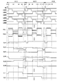
- FIG. 6 is a timing chart showing the operation of the liquid crystal display device. First, the first horizontal period 1H (1) will be described. As shown in FIG. 6, a high level matching instruction signal MA is simultaneously applied to all the discharge circuits 61 of the charge matching circuit 60 at time t1. As a result, all the discharge circuits 61 become conductive, and two source signal lines connected via the discharge circuit 61 are short-circuited by two. As a result, charge redistribution is performed between the shorted source signal lines, and the voltages of the source signal lines SLR1 to SLBm become 0V.
- high level selection signals ASWR1 to ASWRm are respectively applied to the selection circuits 50R1 to 50Rm connected to the source signal lines SLR1 to SLRm to which the display elements 15 functioning as red subpixels are connected.
- the selection circuits 50R1 to 50Rm become conductive, and the positive red video signals output from the source driver 40 to the video signal lines VSL1 to VSLm pass through the selection circuits 50R1 to 50Rm to the source signal lines SLR1 to SLRm. Given to each.
- the selection signals ASWR1 to ASWRm become low level, and at time t3, the gates of the selection circuits 50G1 to 50Gm connected to the source signal lines SLG1 to SLGm to which the display elements 15 functioning as green subpixels are connected are connected. High-level selection signals ASWG1 to ASWGm are respectively provided. As a result, the selection circuits 50G1 to 50Gm are turned on, and the negative green video signals output from the source driver 40 to the video signal lines VSL1 to VSLm are supplied to the source signal lines SLG1 to SLGm via the selection circuits 50G1 to 50Gm. Given to each.
- the selection signals ASWG1 to ASWGm go to a low level, and at time t4, the gates of the selection circuits 50B1 to 50Bm connected to the source signal lines SLB1 to SLBm to which the display elements 15 functioning as blue subpixels are connected are applied. High level selection signals ASWB1 to ASWBm are respectively provided. As a result, the selection circuits 50B1 to 50Bm are turned on, and the positive blue video signals output from the source driver 40 to the video signal lines VSL1 to VSLm are passed through the selection circuits 50B1 to 50Bm to the source signal lines SLB1 to SLBm. Given to each.
- the gate signal line GL1 is a period from when the voltage corresponding to the red video signal is applied to the source signal lines SLR1 to SLRm until the voltage corresponding to the blue video signal is applied to the source signal lines SLB1 to SLBm.
- a high-level scanning signal is applied to.
- a positive red video signal is applied to the pixel capacitor Cp of the red subpixel connected to the gate signal line GL1
- a negative green video signal is applied to the pixel capacitor Cp of the green subpixel.
- a positive blue video signal is applied to the pixel capacitor Cp of the sub-pixel.
- the scanning signal of the gate signal line GL1 is set to a low level.
- the TFT 11 of each subpixel is turned off, the red subpixel and the blue subpixel connected to the gate signal line GL1 store a positive video signal, and the green subpixel stores a negative video signal.
- the source signal lines SLR1 to SLRm and SLB1 to SLBm are given a positive video signal, and the source signal lines SLG1 to SLGm are given a negative video signal.
- the high level selection signals ASWG1 to ASWGm are simultaneously applied to the selection circuits 50G1 to 50Gm, respectively, in order to apply ⁇ 5V to the source signal lines SLG1 to SLGm to which the negative video signals are applied.
- the selection circuits 50G1 to 50Gm become conductive, and ⁇ 5V is applied to the source signal lines SLG1 to SLGm, respectively.
- the voltage of the source signal lines SLG1 to SLGm becomes ⁇ 5 V regardless of the voltage of the green video signal given at time t3.
- the high level selection signals ASWR1 to ASWRm and ASWB1 to ASWBm are selected by the selection circuit 50R1.
- the selection circuits 50R1 to 50Rm and 50B1 to 50Bm become conductive, and +5 V is applied to the source signal lines SLR1 to SLRm and SLB1 to SLBm, respectively.
- the voltages of the source signal lines SLR1 to SLRm and SLB1 to SLBm become + 5V regardless of the voltage of the red or blue video signal applied at time t2 or t4.
- a high-level matching instruction signal MA is simultaneously applied to the discharge circuit 61.
- all the discharge circuits 61 become conductive, and two source signal lines connected via the discharge circuit 61 are short-circuited by two.
- charge redistribution is performed between the shorted source signal lines, and the voltages of the source signal lines SLR1 to SLBm become 0V.
- a video signal obtained by inverting the polarity of the video signal applied in the first horizontal period 1H (1) is given to the source signal lines SLR1 to SLBm.
- a high-level scanning signal is applied to the gate signal line GL2 to activate it, the selection signals ASWR1 to ASWRm are set to high level, and negative red video is applied to the source signal lines SLR1 to SLRm.
- the selection signals ASWG1 to ASWGm are set to a high level, and positive green video signals are given to the source signal lines SLG1 to SLGm.
- the selection signals ASWB1 to ASWBm are set to a high level, and negative blue video signals are supplied to the source signal lines SLB1 to SLBm. Thereafter, the scanning signal applied to the gate signal line GL2 is set to the low level. As a result, the TFT 11 of each subpixel is turned off, the red subpixel and the blue subpixel connected to the gate signal line GL2 store a negative video signal, and the green subpixel stores a positive video signal. To do.
- the source signal lines SLR1 to SLRm and SLB1 to SLBm are given a negative video signal, and the source signal lines SLG1 to SLGm are given a positive video signal.
- the high level selection signals ASWG1 to ASWGm are simultaneously applied to the corresponding selection circuits 50G1 to 50Gm, respectively.
- the selection circuits 50G1 to 50Gm become conductive, and +5 V is applied to the source signal lines SLG1 to SLGm.
- the voltage of the source signal lines SLG1 to SLGm becomes + 5V regardless of the voltage of the green video signal given at time t9.
- the high level selection signals ASWR1 to ASWRm and ASWB1 to ASWBm are applied at time t12.
- the signals are simultaneously applied to the selection circuits 50R1 to 50Rm and 50B1 to 50Bm, respectively.
- the selection circuits 50R1 to 50Rm and 50B1 to 50Bm become conductive, and ⁇ 5V is applied to the source signal lines SLR1 to SLRm and SLB1 to SLBm.
- the voltages of the source signal lines SLR1 to SLRm and SLB1 to SLBm become ⁇ 5V regardless of the voltage of the red or blue video signal applied at time t8 or t10.
- high level matching instruction signal MA is simultaneously applied to discharge circuit 61.
- all the discharge circuits 61 become conductive, and two source signal lines connected via the discharge circuit 61 are short-circuited by two.
- charge redistribution is performed between the shorted source signal lines, and the voltages of the source signal lines SLR1 to SLBm become 0V.
- the next video signal is applied to the source signal lines SLR1 to SLBm whose voltages have become 0V.
- the reset voltage is a voltage having the same absolute value and different polarity, such as + 5V and -5V.
- voltages having the same absolute value and different polarities are, for example, + 5.1V and -5.2V, and if the source signal line is short-circuited, those voltages are close to 0V. It also includes a voltage that has substantially the same effect as the form. The same applies to the liquid crystal display devices according to second and third embodiments described later.
- the source signal line to which +5 V is applied and the source signal line to which ⁇ 5 V is applied are short-circuited, whereby charge is regenerated between the source signal lines. Distribution takes place and their voltage is 0V.
- the voltage of the source signal line is affected by the video signal applied in the immediately preceding one horizontal period.
- the voltage corresponds to the video signal. Therefore, such a liquid crystal display device can display a color image with little display unevenness and high uniformity.
- the selection circuits 50R1 to 50Bm analog switches with low power consumption during driving and high current driving capability are used. As a result, even if there are variations in characteristics of the thin film transistors constituting the analog switch, the source signal lines SLR1 to SLBm can be charged in a short time, so that display unevenness due to insufficient charging of the source signal lines SLR1 to SLBm can be reduced. it can.
- the discharge circuit 61 may be arranged so as to connect two adjacent source signal lines, the liquid crystal display device can be easily designed.
- Second Embodiment> ⁇ 2.1 Configuration of liquid crystal display device>
- the configuration of the liquid crystal display device according to the second embodiment of the present invention is the same as the configuration of the liquid crystal display device according to the first embodiment shown in FIG. Note that the liquid crystal display device according to this embodiment is driven by column inversion, unlike the liquid crystal display device of FIG.
- FIG. 7 is a diagram showing a configuration of the display unit 10 including the multiplexer 50 and the charge matching circuit 65 included in the liquid crystal display device according to the present embodiment. Since the configuration of the multiplexer 50 shown in FIG. 7 is the same as the configuration of the multiplexer 50 shown in FIG. 3, the same reference numerals as those in FIG.
- the charge matching circuit 65 also includes 3 m / 2 discharge circuits 66 formed of analog switches.
- the gate terminal of the N-channel TFT is directly connected to the display control circuit 20, and the gate terminal of the P-channel TFT is connected to the display control circuit 20 via an inverter. If the high-level matching instruction signal MA is given from the display control circuit 20 to the discharge circuit 66, both the N-channel and P-channel TFTs are turned on. As a result, all the discharge circuits 61 become conductive.
- the drain terminal of each TFT is connected to one source signal line of two source signal lines that give the same color video signal in adjacent pixels, and the source terminal is connected to the other source signal line. Yes.
- + 5V is applied to the source signal line SLR1 to which the positive red video signal is applied, and the source signal line SLR2 to which the negative red video signal is applied.
- -5V is applied to. Since the source signal line SLR1 and the source signal line SLR2 are connected via the discharge circuit 66, when the high level matching instruction signal MA is given to the discharge circuit 66 from the display control circuit 20, all the discharge circuits 66 are The conductive state is established, and the source signal line SLR1 and the source signal line SLR2 are short-circuited. As a result, the voltages of the source signal line SLR1 and the source signal line SLR2 are both 0V.
- a source signal line SLG1 and a source signal line SLG2 to which a green video signal is applied, and a source signal line SLB1 and a source signal line SLB2 to which a blue video signal is applied are connected via a discharge circuit 66, respectively. Yes. Therefore, when the high level matching instruction signal MA is applied, all the discharge circuits 66 are turned on. As a result, the source signal line SLG1 and the source signal line SLG2, and the source signal line SLB1 and the source signal line SLB2 are short-circuited, and their voltages are all 0V. In this way, the voltages of the source signal lines SLR1 to SLBm all become 0V.
- the polarity of the reset voltage applied to each of the source signal lines SLR1 to SLBm is the same as that in the first horizontal period 1H (1). Therefore, as in the case of the first horizontal period 1H (1), the voltages of the source signal lines SLR1 to SLBm become 0V for each horizontal period.
- FIG. 8 is a diagram showing source signal lines to which a voltage is applied in each horizontal period by the column inversion driving method. More specifically, FIG. 8A shows each color in the second horizontal period 1H (2).
- FIG. 8B is a diagram showing source signal lines in which video signals are stored in the sub-pixels of FIG. 8B and then a reset voltage is applied, and FIG. 8B is a source signal line short-circuited at the beginning of the third horizontal period 1H (3).
- FIG. 8 is a diagram showing source signal lines to which a voltage
- either of the source signal lines SLR1 to SLRm or the source signal lines SLB1 to SLBm to which the positive red video signal and the blue video signal are given, and the gate signal line GL2 Are stored in the red sub-pixel or blue sub-pixel in the second row connected to.
- a negative green video signal is stored in the second row of green sub-pixels connected to any of the supplied source signal lines SLG1 to SLGm and the gate signal line GL2.
- + 5V is applied to the source signal lines SLR1 to SLRm and the source signal lines SLB1 to SLBm
- ⁇ 5V is applied to the source signal lines SLG1 to SLGm.
- the video signals having the same polarity are stored in the sub-pixels of each color given the video signal to the source signal line. Thereafter, + 5V or -5V is applied to each source signal line, and two of them are short-circuited. In this way, the application of the next video signal to the source signal line at 0 V is repeated.
- FIG. 9 is a timing chart showing the operation of the liquid crystal display device according to the present embodiment. As shown in FIG. 9, the level of each signal in the first horizontal period 1H (1) is the same as the level of each signal in the timing chart shown in FIG. For this reason, the first horizontal period 1H (1) will be briefly described.
- the red subpixel and the blue subpixel connected to the gate signal line GL1 store a positive video signal, and the green subpixel stores a negative video signal. Further, + 5V is applied to the source signal lines SLR1 to SLRm and SLB1 to SLBm, and ⁇ 5V is applied to the source signal lines SLG1 to SLGm.
- the second horizontal period 1H (2) will be described.
- the high-level matching instruction signal MA is simultaneously applied to all the discharge circuits 66 of the charge matching circuit 65.
- all the discharge circuits 66 become conductive, and two source signal lines connected via the discharge circuit 66 are short-circuited by two.
- charge redistribution is performed between the two shorted source signal lines, and the voltages of the source signal lines SLR1 to SLBm become 0V.
- high-level selection signals ASWR1 to ASWRm are applied to the selection circuits 50R1 to 50Rm connected to the source signal lines SLR1 to SLRm to which the display elements functioning as red subpixels are connected, respectively.
- the selection circuits 50R1 to 50Rm become conductive, and the positive red video signals output from the source driver 40 to the video signal lines VSL1 to VSLm pass through the selection circuits 50R1 to 50Rm to the source signal lines SLR1 to SLRm.
- the selection signals ASWR1 to ASWRm go to the low level, and at time t9, the selection circuits 50G1 to 50Gm connected to the source signal lines SLG1 to SLGm connected to the display elements that function as the green subpixel are selected to the high level. Signals ASWG1 to ASWGm are respectively provided. As a result, the selection circuits 50G1 to 50Gm are turned on, and the negative green video signals output from the source driver 40 to the video signal lines VSL1 to VSLm are supplied to the source signal lines SLG1 to SLGm via the selection circuits 50G1 to 50Gm. Given to each.
- the selection signals ASWG1 and ASWG2 are set to the low level, and at time t10, the selection circuits 50B1 to 50Bm connected to the source signal lines SLB1 to SLBm connected to the display elements functioning as the blue subpixels are respectively set to the high level. Selection signals ASWB1 to ASWBm are applied. As a result, the selection circuits 50B1 to 50Bm are turned on, and the positive blue video signals output from the source driver 40 to the video signal lines VSL1 to VSLm are passed through the selection circuits 50B1 to 50Bm to the source signal lines SLB1 to SLBm. Given to each.
- the gate signal line GL2 has a period from when a voltage corresponding to the red video signal is applied to the source signal lines SLR1 to SLRm until a voltage corresponding to the blue video signal is applied to the source signal line SLBm.
- a high level scanning signal is applied.
- a positive red video signal is applied to the pixel capacitance Cp of the red subpixel connected to the gate signal line GL2, and a negative green video signal is applied to the pixel capacitance Cp of the green subpixel.
- a positive blue video signal is applied to the pixel capacitor Cp of the sub-pixel.
- the scanning signal of the gate signal line GL2 is set to the low level.
- the TFT 11 of each subpixel is turned off, the red subpixel and the blue subpixel connected to the gate signal line GL2 store a positive video signal, and the green subpixel stores a negative video signal.
- the source signal lines SLR1 to SLRm and SLB1 to SLBm are given a positive video signal, and the source signal lines SLG1 to SLGm are given a negative video signal.
- the high level selection signals ASWG1 to ASWGm are simultaneously applied to the selection circuits 50G1 to 50Gm, respectively.
- the selection circuits 50G1 to 50Gm become conductive, and ⁇ 5V is applied to the source signal lines SLG1 to SLGm.
- the voltage of the source signal lines SLG1 to SLGm becomes ⁇ 5 V regardless of the voltage of the green video signal given at time t9.
- the high level selection signals ASWR1 to ASWR1 and ASWB1 to ASWBm are selected by the selection circuits 50R1 to 50Rm and 50B1. ⁇ 50 Bm at the same time.
- the selection circuits 50R1 to 50Rm and 50B1 to 50Bm become conductive, and +5 V is applied to the source signal lines SLR1 to SLRm and SLB1 to SLBm.
- the voltages of the source signal lines SLR1 to SLRm and SLB1 to SLBm become + 5V regardless of the voltage of the red or blue video signal applied at time t8 or time t10.
- high-level matching instruction signal MA is applied to discharge circuit 66 at the same time. Thereby, all the discharge circuits 66 are made conductive, and the two source signal lines connected by the discharge circuit 66 are short-circuited. As a result, charge redistribution is performed between the shorted source signal lines, and the voltages of the source signal lines SLR1 to SLBm become 0V. In this way, the next video signal is applied to the source signal lines SLR1 to SLBm whose voltages have become 0V.
- the source signal lines are short-circuited two by two, whereby charge redistribution is performed between the source signal lines, and their voltage becomes 0V.
- the voltage of the source signal line is affected by the video signal applied in the immediately preceding one horizontal period.
- the voltage corresponds to the video signal. Therefore, such a liquid crystal display device can display a color image with little display unevenness and high uniformity.
- a liquid crystal display device driven by column inversion can be used as a monochromatic display device that displays only red video, for example.
- a reset voltage having the same polarity as the voltage corresponding to the video signal is alternately applied only to the source signal lines SLR1 to SLRm to which the video signal representing red is applied, and charge redistribution is performed between them.
- video signals are not applied to the source signal lines SLG1 to SLGm and SLB1 to SLBm. Therefore, it is not necessary to apply a reset voltage to the source signal lines SLG1 to SLGm and SLB1 to SLBm and perform charge redistribution between them.
- the charge redistribution is performed only between the source signal lines SLR1 to SLRm, so that the charge redistribution can be performed efficiently.
- the liquid crystal display device according to the present embodiment is a display device that is driven by dot inversion similarly to the liquid crystal display device according to the first embodiment, a diagram showing dot inversion driving and description thereof are omitted.
- FIG. 10 is a timing chart showing the operation of the liquid crystal display device according to the present embodiment.
- a high level matching instruction signal MA is given from the display control circuit 20 to the charge matching circuit 60 at time t1.
- all the discharge circuits 61 of the charge matching circuit 60 are turned on, and two source signal lines connected via the discharge circuit 61 are short-circuited two by two.
- charge redistribution is performed between the shorted source signal lines, and the voltages of the source signal lines SLR1 to SLBm become 0V.
- a positive video signal is applied to the red subpixel and the blue subpixel, and a negative video signal is applied to the green subpixel. Further, positive red video signals are supplied to the source signal lines SLR1 to SLRm, negative green video signals are supplied to the source signal lines SLG1 to SLGm, and positive blue video signals are supplied to the source signal lines SLB1 to SLBm, respectively. Applied.
- the high level selection signals ASWG1 to ASWGm are simultaneously applied to the corresponding selection circuits 50G1 to 50Gm, respectively. give.
- the selection circuits 50G1 to 50Gm become conductive, and ⁇ 5V is applied to the source signal lines SLG1 to SLGm.
- the voltage of the source signal lines SLG1 to SLGm becomes ⁇ 5 V regardless of the voltage of the green video signal given at time t3.
- the time for applying ⁇ 5V to the source signal lines SLG1 to SLGm is set to the same time as that for applying ⁇ 5V to the source signal lines SLG1 to SLGm at time t5 in FIG.
- the high level selection signals ASWR1 to ASWRm and ASWB1 to ASWBm are selected correspondingly.
- the signals are simultaneously applied to the circuits 50R1 to 50Rm and 50B1 to 50Bm, respectively.
- the selection circuits 50R1 to 50Rm and 50B1 to 50Bm become conductive, and +5 V is applied to the source signal lines SLR1 to SLRm and SLB1 to SLBm.
- the voltages of the source signal lines SLR1 to SLRm and SLB1 to SLBm become + 5V regardless of the voltage of the red or blue video signal applied at time t2 or t4.
- the time for applying + 5V to the source signal lines SLR1 to SLRm and SLB1 to SLBm is set to approximately twice the time for applying ⁇ 5V to the source signal lines SLG1 to SLGm at time t5.
- the second horizontal period 1H (2) will be described.
- the high-level matching instruction signal MA is simultaneously applied to all the discharge circuits 61 of the charge matching circuit 60.
- all the discharge circuits 61 become conductive, and two source signal lines connected via the discharge circuit 61 are short-circuited by two.
- charge redistribution is performed between the shorted source signal lines, and the voltages of the source signal lines SLR1 to SLBm become 0V.
- a negative video signal image is applied to the red subpixel and the blue subpixel, and a positive video signal is applied to the green subpixel.
- negative red video signals are supplied to the source signal lines SLR1 to SLRm
- positive green video signals are supplied to the source signal lines SLG1 to SLGm
- negative blue video signals are supplied to the source signal lines SLB1 to SLBm, respectively.
- high level selection signals ASWG1 to ASWGm are simultaneously applied to the selection circuits 50G1 to 50Gm in order to apply +5 V to the source signal lines SLG1 to SLGm to which the positive video signals are applied.
- the selection circuits 50G1 to 50Gm become conductive, and +5 V is applied to the source signal lines SLG1 to SLGm.
- the time for applying + 5V to the source signal lines SLG1 to SLGm is set to the same time as that for applying ⁇ 5V to the source signal lines SLG1 to SLGm at time t11 in FIG.
- the high level selection signals ASWR1 to ASWRm and ASWB1 to ASWBm are selected.
- 50R1 to 50Rm and 50B1 to 50Bm are respectively given simultaneously.
- the selection circuits 50R1 to 50Rm and 50B1 to 50Bm become conductive, and ⁇ 5V is applied to the source signal lines SLR1 to SLRm and SLB1 to SLBm.
- the voltages of the source signal lines SLR1 to SLRm and SLB1 to SLBm become ⁇ 5V regardless of the voltage of the red or blue video signal applied at time t8 or t10.
- the time for applying ⁇ 5V to the source signal lines SLR1 to SLRm and SLB1 to SLBm is set to approximately twice the time for applying + 5V to the source signal lines SLG1 to SLGm at time t11.
- a high-level matching instruction signal MA is simultaneously applied to all the discharge circuits 61 of the charge matching circuit 60.
- all the discharge circuits 61 become conductive, and two source signal lines connected to the discharge circuit 61 are short-circuited by two.
- charge redistribution is performed between the shorted source signal lines, and the voltages of the source signal lines SLR1 to SLBm become 0V.
- the next video signal is applied to the source signal lines SLR1 to SLBm whose voltages have become 0V.
- the reason why the time for applying the reset voltage to the source signal lines SLR1 to SLRm and the source signal lines SLB1 to SLBm is set longer than the time for applying the reset voltage to the source signal lines SLG1 to SLGm will be described.
- the selection signal ASWG1 is supplied to the selection circuit 50G1
- the source signal line SLG1 is connected to the video signal line VSL1
- the source signal line SLG1 is charged to ⁇ 5V.
- selection signals ASWR1 and ASWB1 are supplied to the selection circuits 50R1 and 50B1, respectively, and the source signal lines SLR1 and SLB1 are simultaneously connected to the video signal line VSL1, I have to charge it.
- the charging time of the two source signal lines SLR1 and SLB1 connected to the video signal line VSL1 is the same as the charging time of the one source signal line SLG1, the source signal line SLR1 to be charged to + 5V.
- the charging time ends before the voltage of SLB1 becomes + 5V, and the source signal lines SLR1 and SLB1 may be charged only to a voltage lower than + 5V. In this case, even if the source signal line SLG1 charged to ⁇ 5V and the source signal line SLR1 charged only to a voltage lower than + 5V are short-circuited, those voltages do not become 0V.
- the time for charging the source signal lines SLR1 and SLB1 connected to the video signal line VSL1 to + 5V is set to be approximately twice the time for charging the source signal line SLG1 to -5V, so that each source The signal lines SLR1 and SLB1 are reliably charged to + 5V, respectively.
- the source signal line SLR1 and the source signal line SLG1 are short-circuited, their voltages become 0V.
- the time for charging the source signal lines SLR1 and SLB1 connected to the video signal line VSL1 to + 5V is not twice the time for charging the source signal line SLG1 to -5V, but approximately twice. It was.
- the reason why it is approximately double is that charging is completed in a short time if the current value for charging the source signal lines SLR1 and SLB1 is large, and on the contrary, if the current value is small, it takes a long time. This is because even if the number of source signal lines is doubled, it is not always necessary to double the time.
- the time for charging the source signal lines SLR1 to SLRm and SLB1 to SLBm connected to the video signal lines VSL1 to VSLm to + 5V or ⁇ 5V is set.
- the voltage of the source signal lines SLR1 to SLB1 can be reliably charged to + 5V or ⁇ 5V by setting the source signal lines SLG1 to SLGm to approximately twice the time for charging to ⁇ 5V or + 5V. If the source signal lines charged in this way are short-circuited, their voltages are surely 0V. As a result, since a voltage corresponding to the next video signal is applied to the source signal line at 0 V, a color image with less display unevenness and higher uniformity can be displayed.
- the time for applying + 5V or ⁇ 5V to the source signal lines SLR1 to SLRm and SLB1 to SLBm is set to the source signal lines SLG1 to SLBm.
- the time during which + 5V or ⁇ 5V is applied to the source signal lines SLR1 to SLRm and SLB1 to SLBm is set to the source signal lines SLG1 to SLGm ⁇ You may make it longer than the time which applies 5V or + 5V. In this case, the same effect as in the case of the present embodiment can be obtained.
- the number of source signal lines to which +5 V is applied is twice the number of source signal lines to which ⁇ 5 V is applied, but is not limited to two times, and may be three times or more, or It may be less than half.
- the time for applying + 5V or ⁇ 5V depending on the number of source signal lines all the source signal lines can be charged until the reset voltage is reached.
- FIG. 11 is a diagram illustrating a configuration of the display unit 10 including the charge matching circuit 60 in the first modification of the liquid crystal display device according to the first embodiment.
- Each component shown in FIG. 11 is given the same reference numeral as the component shown in FIG. 3 or a corresponding reference symbol.
- the liquid crystal display device according to the first embodiment is a liquid crystal display device that can display a color image
- the present invention is also applicable to a liquid crystal display device that cannot display a color image.
- the video signal output from the source driver does not include the video signal of each color
- the video signals and + 5V and ⁇ 5V output from the source driver are directly applied to the source signal lines SL1 to SL.
- the liquid crystal display device according to the present modification can also display an image with little display unevenness and high uniformity.
- liquid crystal display device can display an image with little display unevenness and high uniformity by adopting the same configuration as that of the first modification.
- FIG. 12 is a diagram illustrating a configuration of the display unit 10 including the charge matching circuit 60 in the second modification of the liquid crystal display device according to the first embodiment.
- Each component shown in FIG. 11 is given the same reference numeral as the component shown in FIG. 3 or a corresponding reference symbol.
- the discharge circuit 61 is short-circuited for every two adjacent source signal lines, but the discharge circuit 61 is used for every four adjacent source signal lines. You may short-circuit.
- + 5V is applied to the two source signal lines
- ⁇ 5V is applied to the other two source signal lines. Therefore, these four source signal lines are connected by the discharge circuit 61, and the discharge circuit 61 is brought into conduction to short-circuit them.
- the voltages of the source signal lines SLR1 to SLBm can be set to 0V.
- the liquid crystal display device according to the present modification can also display an image with little display unevenness and high uniformity.
- the number of source signal lines connected by the discharge circuit 61 is not limited to two or four as long as the number of source signal lines to which + 5V is applied is equal to the number of source signal lines to which ⁇ 5V is applied.
- the liquid crystal display device according to the second embodiment can display an image with little display unevenness and high uniformity by adopting the same configuration as that of the first modification.
- the liquid crystal display device has been described as an example.
- the present invention is not limited to this, and can be applied to an organic EL (Electro Luminescence) display device or the like.
- the present invention is applied to a matrix display device such as an active matrix liquid crystal display device, and is particularly suitable for a display device that performs charge redistribution.
- SYMBOLS 10 Display part 15 ... Display element 30 ... Gate driver (scanning signal line drive circuit) 40 ... Source driver (data signal line drive circuit) 50 ... Multiplexer 50R1-50Bm ... Selection circuit 60, 65 ... Charge matching circuit 61, 66 ... Discharge circuit VSL1-VSLm ... Video signal line SLR1-SLBm ... Source signal line (sub data signal line) SL1 to SLm ... Source signal line (data signal line) GL1 to GLn: Gate signal lines (scanning signal lines) ASWR1 to ASWBm ... selection signal MA ... matching signal
Landscapes
- Engineering & Computer Science (AREA)
- Chemical & Material Sciences (AREA)
- Crystallography & Structural Chemistry (AREA)
- Physics & Mathematics (AREA)
- Computer Hardware Design (AREA)
- General Physics & Mathematics (AREA)
- Theoretical Computer Science (AREA)
- Control Of Indicators Other Than Cathode Ray Tubes (AREA)
- Liquid Crystal Display Device Control (AREA)
Abstract
La présente invention vise à proposer un dispositif d'affichage dans lequel l'uniformité d'une image affichée après répartition des charges n'est pas perdue ; et un procédé d'alimentation de celui-ci. Durant une première période horizontale, une tension positive et une tension négative correspondant à un signal d'image sont alternativement appliquées à chaque ligne de signal de source, et ensuite des tensions de réinitialisation de +5 V et de -5 V sont appliquées à chaque ligne de signal de source. En résultat, les tensions des lignes de signal de source sont de +5 V ou -5 V. Dans cet état, au début de la seconde période horizontale, un court-circuitage des lignes de signal de source auxquelles des tensions de +5 V et de -5 V ont été appliquées amène une répartition des charges à être effectuée entre les lignes de signal de source, et leur tension devient de 0 V. Ensuite, l'application d'une tension correspondant au signal d'image amène un dispositif LCD à être apte à afficher une image couleur ayant une uniformité élevée et ayant une faible quantité d'irrégularités d'affichage.
Priority Applications (1)
| Application Number | Priority Date | Filing Date | Title |
|---|---|---|---|
| US14/349,785 US9595233B2 (en) | 2011-10-11 | 2012-10-04 | Display device and driving method thereof |
Applications Claiming Priority (2)
| Application Number | Priority Date | Filing Date | Title |
|---|---|---|---|
| JP2011-223789 | 2011-10-11 | ||
| JP2011223789 | 2011-10-11 |
Publications (1)
| Publication Number | Publication Date |
|---|---|
| WO2013054724A1 true WO2013054724A1 (fr) | 2013-04-18 |
Family
ID=48081780
Family Applications (1)
| Application Number | Title | Priority Date | Filing Date |
|---|---|---|---|
| PCT/JP2012/075747 Ceased WO2013054724A1 (fr) | 2011-10-11 | 2012-10-04 | Dispositif d'affichage et procédé d'alimentation de celui-ci |
Country Status (2)
| Country | Link |
|---|---|
| US (1) | US9595233B2 (fr) |
| WO (1) | WO2013054724A1 (fr) |
Cited By (2)
| Publication number | Priority date | Publication date | Assignee | Title |
|---|---|---|---|---|
| CN104599644A (zh) * | 2013-10-30 | 2015-05-06 | 联咏科技股份有限公司 | 等化方法及其驱动装置 |
| WO2025100217A1 (fr) * | 2023-11-08 | 2025-05-15 | ソニーセミコンダクタソリューションズ株式会社 | Dispositif d'affichage |
Families Citing this family (6)
| Publication number | Priority date | Publication date | Assignee | Title |
|---|---|---|---|---|
| KR102219667B1 (ko) * | 2014-09-17 | 2021-02-24 | 엘지디스플레이 주식회사 | 표시장치 |
| CN104280960B (zh) * | 2014-10-21 | 2017-04-26 | 深圳市华星光电技术有限公司 | 液晶面板及其驱动方法、液晶显示器 |
| CN107357099B (zh) * | 2016-05-10 | 2021-05-07 | 群创光电股份有限公司 | 面板装置及其驱动方法 |
| KR102509164B1 (ko) * | 2016-09-29 | 2023-03-13 | 엘지디스플레이 주식회사 | 표시장치 및 그를 이용한 서브픽셀 트랜지션 방법 |
| CN113160733B (zh) * | 2020-01-22 | 2023-05-30 | 群创光电股份有限公司 | 电子装置 |
| KR20240068895A (ko) * | 2022-11-10 | 2024-05-20 | 삼성디스플레이 주식회사 | 표시 장치 |
Citations (3)
| Publication number | Priority date | Publication date | Assignee | Title |
|---|---|---|---|---|
| JP2001134245A (ja) * | 1999-11-10 | 2001-05-18 | Sony Corp | 液晶表示装置 |
| WO2004047067A1 (fr) * | 2002-11-20 | 2004-06-03 | Mitsubishi Denki Kabushiki Kaisha | Appareil d'affichage d'images |
| JP2008008928A (ja) * | 2006-06-27 | 2008-01-17 | Mitsubishi Electric Corp | 液晶表示装置及びその駆動方法 |
Family Cites Families (4)
| Publication number | Priority date | Publication date | Assignee | Title |
|---|---|---|---|---|
| JPH1130975A (ja) | 1997-05-13 | 1999-02-02 | Oki Electric Ind Co Ltd | 液晶表示装置の駆動回路及びその駆動方法 |
| JP2000148098A (ja) | 1998-11-13 | 2000-05-26 | Ind Technol Res Inst | 液晶ディスプレーの周辺回路 |
| JP4610843B2 (ja) * | 2002-06-20 | 2011-01-12 | カシオ計算機株式会社 | 表示装置及び表示装置の駆動方法 |
| TWI383231B (zh) * | 2009-02-27 | 2013-01-21 | Hannstar Display Corp | 像素結構及其驅動方法 |
-
2012
- 2012-10-04 US US14/349,785 patent/US9595233B2/en active Active
- 2012-10-04 WO PCT/JP2012/075747 patent/WO2013054724A1/fr not_active Ceased
Patent Citations (3)
| Publication number | Priority date | Publication date | Assignee | Title |
|---|---|---|---|---|
| JP2001134245A (ja) * | 1999-11-10 | 2001-05-18 | Sony Corp | 液晶表示装置 |
| WO2004047067A1 (fr) * | 2002-11-20 | 2004-06-03 | Mitsubishi Denki Kabushiki Kaisha | Appareil d'affichage d'images |
| JP2008008928A (ja) * | 2006-06-27 | 2008-01-17 | Mitsubishi Electric Corp | 液晶表示装置及びその駆動方法 |
Cited By (2)
| Publication number | Priority date | Publication date | Assignee | Title |
|---|---|---|---|---|
| CN104599644A (zh) * | 2013-10-30 | 2015-05-06 | 联咏科技股份有限公司 | 等化方法及其驱动装置 |
| WO2025100217A1 (fr) * | 2023-11-08 | 2025-05-15 | ソニーセミコンダクタソリューションズ株式会社 | Dispositif d'affichage |
Also Published As
| Publication number | Publication date |
|---|---|
| US9595233B2 (en) | 2017-03-14 |
| US20140267473A1 (en) | 2014-09-18 |
Similar Documents
| Publication | Publication Date | Title |
|---|---|---|
| US10242634B2 (en) | Display device | |
| EP2199850B1 (fr) | Ecran à cristaux liquides avec des paires de pixel utilisant une ligne de commande commune | |
| US9934736B2 (en) | Liquid crystal display and method for driving the same | |
| KR101127593B1 (ko) | 액정 표시 장치 | |
| KR102127510B1 (ko) | 표시장치 | |
| CN101271210B (zh) | 液晶显示器件及其驱动方法 | |
| EP3392870B1 (fr) | Circuit de pixels, son procédé d'excitation, circuit d'excitation et dispositif d'affichage | |
| US9035930B2 (en) | Display device and driving method thereof | |
| WO2013054724A1 (fr) | Dispositif d'affichage et procédé d'alimentation de celui-ci | |
| US20120327137A1 (en) | Display device and display driving method | |
| US9293100B2 (en) | Display apparatus and method of driving the same | |
| EP2874002A1 (fr) | Substrat matriciel, affichage à cristaux liquides et son procédé de pilotage | |
| KR20110067227A (ko) | 액정표시장치 및 그 구동방법 | |
| US20200081309A1 (en) | Display device | |
| JP2014186158A (ja) | 表示装置 | |
| KR20110070178A (ko) | 액정 표시장치의 구동장치와 그 구동방법 | |
| WO2017208954A1 (fr) | Circuit de pilotage de ligne de signal vidéo, dispositif d'affichage le comprenant et procédé de pilotage de ligne de signal vidéo | |
| KR20100118356A (ko) | 액정 표시 장치 및 그 구동 방법 | |
| KR20080057501A (ko) | 액정표시장치 및 이의 구동방법 | |
| CN106502008B (zh) | 液晶显示装置以及液晶显示方法 | |
| US20070013631A1 (en) | Liquid crystal display driving methodology with improved power consumption | |
| US8913046B2 (en) | Liquid crystal display and driving method thereof | |
| KR20080086617A (ko) | 액정표시장치 및 이의 구동방법 | |
| TW201333610A (zh) | 顯示裝置及其驅動方法 | |
| JP4781884B2 (ja) | 液晶表示パネルおよびそれを含む液晶表示装置 |
Legal Events
| Date | Code | Title | Description |
|---|---|---|---|
| 121 | Ep: the epo has been informed by wipo that ep was designated in this application |
Ref document number: 12839234 Country of ref document: EP Kind code of ref document: A1 |
|
| WWE | Wipo information: entry into national phase |
Ref document number: 14349785 Country of ref document: US |
|
| NENP | Non-entry into the national phase |
Ref country code: DE |
|
| 122 | Ep: pct application non-entry in european phase |
Ref document number: 12839234 Country of ref document: EP Kind code of ref document: A1 |
|
| NENP | Non-entry into the national phase |
Ref country code: JP |