WO2013054724A1 - Display device and method for powering same - Google Patents
Display device and method for powering same Download PDFInfo
- Publication number
- WO2013054724A1 WO2013054724A1 PCT/JP2012/075747 JP2012075747W WO2013054724A1 WO 2013054724 A1 WO2013054724 A1 WO 2013054724A1 JP 2012075747 W JP2012075747 W JP 2012075747W WO 2013054724 A1 WO2013054724 A1 WO 2013054724A1
- Authority
- WO
- WIPO (PCT)
- Prior art keywords
- signal lines
- data signal
- signal line
- voltage
- sub
- Prior art date
- Legal status (The legal status is an assumption and is not a legal conclusion. Google has not performed a legal analysis and makes no representation as to the accuracy of the status listed.)
- Ceased
Links
Images


Classifications
-
- G—PHYSICS
- G09—EDUCATION; CRYPTOGRAPHY; DISPLAY; ADVERTISING; SEALS
- G09G—ARRANGEMENTS OR CIRCUITS FOR CONTROL OF INDICATING DEVICES USING STATIC MEANS TO PRESENT VARIABLE INFORMATION
- G09G3/00—Control arrangements or circuits, of interest only in connection with visual indicators other than cathode-ray tubes
- G09G3/20—Control arrangements or circuits, of interest only in connection with visual indicators other than cathode-ray tubes for presentation of an assembly of a number of characters, e.g. a page, by composing the assembly by combination of individual elements arranged in a matrix no fixed position being assigned to or needed to be assigned to the individual characters or partial characters
- G09G3/34—Control arrangements or circuits, of interest only in connection with visual indicators other than cathode-ray tubes for presentation of an assembly of a number of characters, e.g. a page, by composing the assembly by combination of individual elements arranged in a matrix no fixed position being assigned to or needed to be assigned to the individual characters or partial characters by control of light from an independent source
- G09G3/36—Control arrangements or circuits, of interest only in connection with visual indicators other than cathode-ray tubes for presentation of an assembly of a number of characters, e.g. a page, by composing the assembly by combination of individual elements arranged in a matrix no fixed position being assigned to or needed to be assigned to the individual characters or partial characters by control of light from an independent source using liquid crystals
- G09G3/3611—Control of matrices with row and column drivers
- G09G3/3685—Details of drivers for data electrodes
- G09G3/3688—Details of drivers for data electrodes suitable for active matrices only
-
- G—PHYSICS
- G09—EDUCATION; CRYPTOGRAPHY; DISPLAY; ADVERTISING; SEALS
- G09G—ARRANGEMENTS OR CIRCUITS FOR CONTROL OF INDICATING DEVICES USING STATIC MEANS TO PRESENT VARIABLE INFORMATION
- G09G3/00—Control arrangements or circuits, of interest only in connection with visual indicators other than cathode-ray tubes
- G09G3/20—Control arrangements or circuits, of interest only in connection with visual indicators other than cathode-ray tubes for presentation of an assembly of a number of characters, e.g. a page, by composing the assembly by combination of individual elements arranged in a matrix no fixed position being assigned to or needed to be assigned to the individual characters or partial characters
- G09G3/34—Control arrangements or circuits, of interest only in connection with visual indicators other than cathode-ray tubes for presentation of an assembly of a number of characters, e.g. a page, by composing the assembly by combination of individual elements arranged in a matrix no fixed position being assigned to or needed to be assigned to the individual characters or partial characters by control of light from an independent source
- G09G3/36—Control arrangements or circuits, of interest only in connection with visual indicators other than cathode-ray tubes for presentation of an assembly of a number of characters, e.g. a page, by composing the assembly by combination of individual elements arranged in a matrix no fixed position being assigned to or needed to be assigned to the individual characters or partial characters by control of light from an independent source using liquid crystals
- G09G3/3611—Control of matrices with row and column drivers
- G09G3/3648—Control of matrices with row and column drivers using an active matrix
- G09G3/3659—Control of matrices with row and column drivers using an active matrix the addressing of the pixel involving the control of two or more scan electrodes or two or more data electrodes, e.g. pixel voltage dependant on signal of two data electrodes
-
- G—PHYSICS
- G09—EDUCATION; CRYPTOGRAPHY; DISPLAY; ADVERTISING; SEALS
- G09G—ARRANGEMENTS OR CIRCUITS FOR CONTROL OF INDICATING DEVICES USING STATIC MEANS TO PRESENT VARIABLE INFORMATION
- G09G3/00—Control arrangements or circuits, of interest only in connection with visual indicators other than cathode-ray tubes
- G09G3/20—Control arrangements or circuits, of interest only in connection with visual indicators other than cathode-ray tubes for presentation of an assembly of a number of characters, e.g. a page, by composing the assembly by combination of individual elements arranged in a matrix no fixed position being assigned to or needed to be assigned to the individual characters or partial characters
- G09G3/34—Control arrangements or circuits, of interest only in connection with visual indicators other than cathode-ray tubes for presentation of an assembly of a number of characters, e.g. a page, by composing the assembly by combination of individual elements arranged in a matrix no fixed position being assigned to or needed to be assigned to the individual characters or partial characters by control of light from an independent source
- G09G3/36—Control arrangements or circuits, of interest only in connection with visual indicators other than cathode-ray tubes for presentation of an assembly of a number of characters, e.g. a page, by composing the assembly by combination of individual elements arranged in a matrix no fixed position being assigned to or needed to be assigned to the individual characters or partial characters by control of light from an independent source using liquid crystals
- G09G3/3607—Control arrangements or circuits, of interest only in connection with visual indicators other than cathode-ray tubes for presentation of an assembly of a number of characters, e.g. a page, by composing the assembly by combination of individual elements arranged in a matrix no fixed position being assigned to or needed to be assigned to the individual characters or partial characters by control of light from an independent source using liquid crystals for displaying colours or for displaying grey scales with a specific pixel layout, e.g. using sub-pixels
-
- G—PHYSICS
- G09—EDUCATION; CRYPTOGRAPHY; DISPLAY; ADVERTISING; SEALS
- G09G—ARRANGEMENTS OR CIRCUITS FOR CONTROL OF INDICATING DEVICES USING STATIC MEANS TO PRESENT VARIABLE INFORMATION
- G09G2310/00—Command of the display device
- G09G2310/02—Addressing, scanning or driving the display screen or processing steps related thereto
- G09G2310/0243—Details of the generation of driving signals
- G09G2310/0248—Precharge or discharge of column electrodes before or after applying exact column voltages
-
- G—PHYSICS
- G09—EDUCATION; CRYPTOGRAPHY; DISPLAY; ADVERTISING; SEALS
- G09G—ARRANGEMENTS OR CIRCUITS FOR CONTROL OF INDICATING DEVICES USING STATIC MEANS TO PRESENT VARIABLE INFORMATION
- G09G3/00—Control arrangements or circuits, of interest only in connection with visual indicators other than cathode-ray tubes
- G09G3/20—Control arrangements or circuits, of interest only in connection with visual indicators other than cathode-ray tubes for presentation of an assembly of a number of characters, e.g. a page, by composing the assembly by combination of individual elements arranged in a matrix no fixed position being assigned to or needed to be assigned to the individual characters or partial characters
- G09G3/34—Control arrangements or circuits, of interest only in connection with visual indicators other than cathode-ray tubes for presentation of an assembly of a number of characters, e.g. a page, by composing the assembly by combination of individual elements arranged in a matrix no fixed position being assigned to or needed to be assigned to the individual characters or partial characters by control of light from an independent source
- G09G3/36—Control arrangements or circuits, of interest only in connection with visual indicators other than cathode-ray tubes for presentation of an assembly of a number of characters, e.g. a page, by composing the assembly by combination of individual elements arranged in a matrix no fixed position being assigned to or needed to be assigned to the individual characters or partial characters by control of light from an independent source using liquid crystals
- G09G3/3611—Control of matrices with row and column drivers
- G09G3/3614—Control of polarity reversal in general
Definitions
- the present invention relates to a display device and a driving method thereof, and more particularly to a display device that performs charge redistribution (charge sharing) and a driving method thereof.
- a dot voltage is applied to a counter electrode of each pixel to alternately apply a positive video signal and a negative video signal for each source signal line.
- Image display quality is improved by performing inversion driving or column inversion driving.
- a discharge circuit is provided for each of two adjacent source signal lines, and the discharge circuits are simultaneously turned on every horizontal period. At this time, a positive video signal is given to one source signal line, and a negative video signal is given to the other source signal line. Charge redistribution is performed. The charge redistribution reduces the swing width of the video signal required when inverting the polarity of the video signal, thereby reducing power consumption.
- the voltage corresponding to the video signal applied to each source signal line is different for each video signal, the voltage of the source signal line after charge redistribution between two adjacent source signal lines is different each time. . That is, the voltage of the source signal line after charge redistribution becomes 0V, a positive voltage, or a negative voltage. Even if the next video signal is applied to such a source signal line, the voltage of the source signal line is affected by the voltage after charge redistribution and may be higher or lower than the voltage of the applied video signal. There is a case. In such a case, there is a problem that the uniformity of the image displayed on the display unit is impaired.
- an object of the present invention is to provide a display device in which the uniformity of an image displayed after charge redistribution is not impaired, and a driving method thereof.
- a first aspect of the present invention is an active matrix display device,
- the plurality of data signal lines, the plurality of scanning signal lines intersecting with the plurality of data signal lines, and the intersections of the plurality of data signal lines and the plurality of scanning signal lines are arranged in a matrix.
- a display unit having a plurality of pixels; A scanning signal line driving circuit for sequentially selecting and activating the plurality of scanning signal lines; A data signal line driving circuit for alternately applying a positive voltage and a negative voltage for each data signal line; A plurality of discharge circuits that connect the same number of data signal lines to which a positive voltage is applied and the data signal lines to which a negative voltage is applied; The data signal line driving circuit alternately applies a positive voltage and a negative voltage corresponding to the video signal for each data signal line, and then the absolute value is equal and the polarity corresponds to the video signal.
- a first reset voltage equal to the voltage is applied to each of the data signal lines;
- the discharge circuit may be short-circuited for each data signal line connected to the discharge circuit after the first reset voltage is applied to the data signal line every horizontal period.
- a selection circuit for dividing the video signal including a plurality of color video signals each representing a plurality of colors of video into each color video signal;
- the pixels arranged in the display unit include a plurality of sub-pixels corresponding to the plurality of color video signals,
- the data signal line includes a video signal line for time-dividing and outputting the plurality of color video signals, and a plurality of sub data signal lines respectively connected to the plurality of sub pixels.
- the selection circuit applies voltages corresponding to the plurality of color video signals to the plurality of sub data signal lines, respectively.
- the discharge circuit connects the same number of sub data signal lines to which a positive voltage is applied and sub data signal lines to which a negative voltage is applied,
- the data signal line driving circuit alternately applies a positive voltage and a negative voltage corresponding to the color video signal for each sub data signal line, and then the absolute value is equal and the polarity is the color video.
- a second reset voltage that is the same as the voltage corresponding to the signal is applied to each of the sub data signal lines;
- the discharge circuit may be short-circuited for each sub-data signal line connected to the discharge circuit after the second reset voltage is applied to the sub-data signal line every horizontal period.
- the time for applying the second reset voltage to the sub data signal line is longer according to the number of sub data signal lines connected to each video signal line.
- the absolute value of the second reset voltage is less than or equal to the absolute value of the maximum voltage and the minimum voltage according to the color video signal.
- the selection circuit is constituted by an analog switch.
- the discharge circuit connects two adjacent sub data signal lines.
- the discharge circuit connects the two closest sub data signal lines among the sub data signal lines to which the color video signal of the same color is applied.
- the pixel includes a red subpixel, a green subpixel, and a blue subpixel.
- a ninth aspect of the present invention is the eighth aspect of the present invention,
- the sub-data signal line connected to the red sub-pixel and the sub-data signal line connected to the blue sub-pixel and the sub-data signal line connected to the green sub-pixel have different polarities.
- a second reset voltage is applied;
- the time for applying the second reset voltage to the sub-data signal line connected to the red sub-pixel and the sub-data signal line connected to the blue sub-pixel is the sub-data connected to the green sub-pixel.
- the time is longer than the time for applying the second reset voltage to the data signal line.
- the data signal line driving circuit performs dot inversion driving.
- An eleventh aspect of the present invention is the second aspect of the present invention,
- the data signal line driving circuit performs column inversion driving.
- a plurality of data signal lines, a plurality of scanning signal lines intersecting with the plurality of data signal lines, and intersections of the plurality of data signal lines and the plurality of scanning signal lines are respectively provided.
- a display unit having a plurality of pixels correspondingly arranged in a matrix;
- a scanning signal line driving circuit for sequentially selecting and activating the plurality of scanning signal lines;
- a data signal line driving circuit for alternately applying a positive voltage and a negative voltage for each data signal line;
- Driving an active matrix display device comprising: the data signal line to which a positive voltage is applied; and a plurality of discharge circuits that connect the same number of data signal lines to which a negative voltage is applied.
- a method A first voltage application step of alternately applying a positive voltage and a negative voltage corresponding to the video signal for each data signal line; After applying a positive voltage and a negative voltage corresponding to the video signal, a first reset voltage having the same absolute value and the same polarity as the voltage corresponding to the video signal is applied to the data signal line.
- a second voltage application step A short-circuiting step for short-circuiting each data signal line connected to the discharge circuit by conducting the discharge circuit after applying the first reset voltage every horizontal period.
- a thirteenth aspect of the present invention is the twelfth aspect of the present invention,
- a selection circuit for dividing the video signal including a plurality of color video signals each representing a plurality of colors of video into each color video signal;
- the pixels arranged in the display unit include a plurality of sub-pixels corresponding to the plurality of colors,
- the data signal line includes a video signal line for time-dividing and outputting the plurality of color video signals, and a plurality of sub data signal lines respectively connected to the sub-pixels.
- the first voltage application step a positive voltage and a negative voltage corresponding to the plurality of color video signals are alternately applied to the plurality of sub data signal lines
- the second voltage applying step after applying voltages corresponding to the plurality of color video signals to the plurality of sub data signal lines, the absolute values are equal and the polarities are the same as the voltages corresponding to the color video signals.
- the second reset voltage is applied every horizontal period, and then the sub-data signal line connected to the discharge circuit is short-circuited.
- a positive voltage and a negative voltage corresponding to the video signal are alternately applied to each data signal line every horizontal period.
- a first reset voltage having the same absolute value and the same polarity as the voltage corresponding to the video signal is applied to each data signal line.
- the first reset voltage having the same absolute value and different polarity is alternately applied to each data signal line. In this state, when the data signal line to which the first reset voltage is applied is short-circuited, charge redistribution is performed between the data signal lines, and these voltages become 0V.
- the positive voltage and the negative voltage corresponding to the color video signal are alternately applied to the sub-data signal lines every horizontal period.
- a second reset voltage having the same absolute value and the same polarity as the voltage corresponding to the color video signal is applied to the sub data signal line.
- a second reset voltage having the same absolute value and different polarity is applied alternately to each sub data signal line, not the voltage corresponding to the color video signal line.
- the display device can display a color image with little display unevenness and high uniformity.
- the second reset voltage is simultaneously applied from one video signal line to one or more sub data signal lines with the same polarity. Therefore, when the number of sub data signal lines to which the second reset voltage is applied is large, it is necessary to lengthen the time for charging the voltages of these sub data signal lines to the second reset voltage at the same time. As described above, the charging time is lengthened according to the number of the sub data signal lines, and the voltages of all the sub data signal lines are charged until the second reset voltage is reached. The absolute values of the different voltages are equal. Next, the sub data signal lines charged with the second reset voltages having different polarities are short-circuited, and those voltages are set to 0V. Accordingly, the display device can display a color image with little display unevenness and high uniformity.
- the absolute value of the second reset voltage is smaller than the absolute value of the maximum value and the minimum value of the voltage according to the video signal, data when generating the second reset voltage
- the power consumption of the signal line driver circuit can be reduced.
- the analog switch is a switch with low power consumption during driving and high current driving capability. Therefore, if an analog switch is used as the selection circuit, the sub data signal line can be charged in a short time even if the characteristics of the thin film transistors constituting the analog switch vary. As a result, the sub data signal line can be charged to the second reset voltage in a short time, so that display unevenness due to insufficient charging of the sub data signal line can be reduced.
- the discharge circuit may be arranged so as to connect two adjacent sub data signal lines, the display device can be easily designed.
- a display device in which two closest sub data signal lines among sub data signal lines to which a color video signal of the same color is given is connected by a discharge circuit is connected to a specific color.
- the second reset voltage is applied only to the sub-data signal line to which the color video signal representing a specific color is applied, and the color video signal is not applied to the other sub-data signal lines.
- the second reset voltage is not applied to the data signal line. In such a case, charge redistribution is performed only between sub-data signal lines to which a color video signal representing a specific color is applied, so that charge redistribution can be performed efficiently.
- the display device can display a color image.
- the time for simultaneously applying the second reset voltage to the sub-data signal lines connected to the red sub-pixel and the blue sub-pixel is set to the sub-data signal line connected to the green sub-pixel.
- the time is longer than the time for applying the second reset voltage.
- a display device including a data signal line driving circuit that performs dot inversion driving displays a short circuit by a sub data signal line to which a second reset voltage having a different polarity is applied. An image with little unevenness and high uniformity can be displayed.
- a display device including a data signal line driving circuit that performs column inversion driving displays a display by short-circuiting a sub data signal line to which a second reset voltage having a different polarity is applied. An image with little unevenness and high uniformity can be displayed.
- FIG. 1 is a block diagram illustrating a configuration of a liquid crystal display device according to a first embodiment of the present invention. It is a figure which shows the structure of the display element arrange
- FIG. 2 is a diagram showing source signal lines to which a voltage is applied in each horizontal period by the dot inversion driving method in the liquid crystal display device shown in FIG. 1, and more specifically, (A) shows a sub-color of each color in the first horizontal period.
- FIG. 2 is a diagram showing source signal lines to which a voltage is applied in each horizontal period by the dot inversion driving method in the liquid crystal display device shown in FIG. 1, and more specifically, (A) shows the sub-colors of each color in the second horizontal period. It is a figure which shows the source signal line which memorize
- FIG. 2 is a timing chart illustrating an operation of the liquid crystal display device illustrated in FIG. 1. It is a figure which shows the structure of the display part containing the multiplexer contained in the liquid crystal display device which concerns on 2nd Embodiment, and an electric charge matching circuit.
- the liquid crystal display device according to the second embodiment it is a diagram showing a source signal line to which a voltage is applied in each horizontal period by the column inversion driving method, and more specifically, (A) is in the second horizontal period. It is a figure which shows the source signal line which memorize
- FIG. 6 is a timing chart illustrating an operation of the liquid crystal display device according to the second embodiment.
- 10 is a timing chart illustrating an operation of a liquid crystal display device according to a third embodiment. It is a figure which shows the structure of the display part containing the electric charge matching circuit in the 1st modification of the liquid crystal display device shown in FIG. It is a figure which shows the structure of the display part containing the electric charge matching circuit in the 2nd modification of the liquid crystal display device shown in FIG.
- FIG. 1 is a block diagram showing the configuration of the liquid crystal display device according to the first embodiment of the present invention.
- 1 includes a display unit (liquid crystal panel) 10, a display control circuit 20, a gate driver (scanning signal line driving circuit) 30, a source driver (data signal line driving circuit) 40, a multiplexer 50, and charge matching.
- a circuit 60 is provided.
- m and n are integers of 1 or more, i is an integer of 1 to 3 m, and j is an integer of 1 to n.
- the display unit 10 includes (n ⁇ 3m) display elements 15, n gate signal lines GL1 to GLn, 3m source signal lines SLR1 to SLRm, SLG1 to SLGm, SLB1 to SLBm (hereinafter, “SLR1”). ⁇ SLBm ").
- the (n ⁇ 3 m) display elements 15 have the same shape and the same size, and are 3 m in the row direction (horizontal direction in FIG. 1) and n in the column direction (vertical direction in FIG. 1). Arranged in a shape.
- the n gate signal lines GL1 to GLn are arranged in parallel to each other, and the 3m source signal lines SLR1 to SLBm are arranged in parallel to each other in a direction orthogonal to the gate signal lines GL1 to GLn.
- the 3m display elements 15 arranged in the same row are commonly connected to any one of the n gate signal lines GL1 to GLn.
- the n display elements 15 arranged in the same column are commonly connected to any of the 3m source signal lines SLR1 to SLBm.
- the n gate signal lines GL1 to GLn are referred to as scanning signal lines
- the 3m source signal lines SLR1 to SLBm are referred to as sub data signal lines
- the video signal lines and the source signal lines corresponding to the video signal lines.
- the three display elements 15 arranged continuously in the row direction in the display unit 10 are provided with color filters (not shown) that transmit light of different colors. These three display elements 15 function as a red subpixel, a green subpixel, and a blue subpixel, respectively, and three form one pixel. In FIG. 1, the display elements 15 described as R, G, and B function as a red subpixel, a green subpixel, and a blue subpixel, respectively.
- the display control circuit 20 controls the operation of the liquid crystal display device. More specifically, the display control circuit 20 receives a video signal DAT and a timing signal group TG such as a horizontal synchronization signal and a vertical synchronization signal sent from the outside, and sends a digital video signal DV (hereinafter, “video” to the source driver 40.
- a source start pulse signal SSP for controlling video display on the display unit 10 a source clock signal SCK, and a latch strobe signal LS.
- the gate driver 30 outputs a gate start pulse signal GSP as a scanning start signal and a gate clock signal GCK.
- the display control circuit 20 also supplies the multiplexer 50 with selection signals ASWR1 to ASWRm, ASWG1 to ASWGm, and ASWB1 to ASWBm (hereinafter referred to as “the source signal lines SLR1 to SLBm” for outputting voltages corresponding to the video signals).
- ASWR1 to ASWBm selection signals ASWR1 to ASWRm, ASWG1 to ASWGm, and ASWB1 to ASWBm (hereinafter referred to as “the source signal lines SLR1 to SLBm” for outputting voltages corresponding to the video signals).
- ASWR1 to ASWBm a matching instruction signal MA for charge redistribution between two adjacent source signal lines is output to the charge matching circuit 60.
- the gate driver 30 Based on the gate start pulse signal GSP and the gate clock signal GCK, the gate driver 30 sequentially selects one gate signal line from the n gate signal lines GL1 to GLn, and sets the selected gate signal line to the high level. Provides a level scanning signal. As a result, the selected gate signal line is activated, and among the display elements 15 arranged in the display unit 10, 3m display elements 15 arranged in the same row are selected at once.
- the source driver 40 Based on the source start pulse signal SSP, the source clock signal SCK, and the latch strobe signal LS, the source driver 40 applies m video signal lines VSL1 to VSLm to any one of red, green, and blue video signals. Is applied in a time-sharing manner. In order to perform dot inversion driving, the source driver 40 changes the polarity of the voltage corresponding to the video signal applied to the source signal line from positive to negative or negative from frame period, horizontal period, and source signal line. Invert to positive.
- the multiplexer 50 applies voltages corresponding to the video signals of the respective colors to the corresponding source signal lines based on the selection signals ASWR1 to ASWBm given from the display control circuit 20. Specifically, the multiplexer 50 simultaneously applies voltages corresponding to the red video signals applied to the video signal lines VSL1 to VSLm to the source signal lines SLR1 to SLRm when the selection signals ASWR1 to ASWRm become high level. Apply. Next, when the selection signals ASWG1 to ASWGm are at a high level, voltages corresponding to the green video signals applied to the video signal lines VSL1 to VSLm are simultaneously applied to the source signal lines SLG1 to SLGm. Next, when the selection signals ASWB1 to ASWBm are at a high level, voltages corresponding to the blue video signals applied to the video signal lines VSL1 to VSLm are simultaneously applied to the source signal lines SLB1 to SLBm.
- FIG. 2 is a diagram showing a configuration of the display element 15 arranged in the display unit 10.
- the display element 15 has an N-channel type in which a gate terminal is connected to a gate signal line GLj passing through a corresponding intersection and a source terminal is connected to a source signal line SLi passing through the intersection.
- a liquid crystal capacitor formed by the pixel electrode Ep and the counter electrode Ec constitutes a pixel capacitor Cp.
- the pixel capacitor Cp also has an auxiliary capacitor arranged in parallel with the liquid crystal capacitor so that a video signal can be reliably stored.
- the auxiliary capacitor is not directly related to the present invention, in the present specification, the pixel capacitor Cp will be described as being composed of only a liquid crystal capacitor.
- the TFT 11 may be a P-channel TFT.
- the display element 15 connected to the jth gate signal line GLj and the ith source signal line SLi while the jth gate signal line GLj is activated, the ith source signal line SLi and the pixel electrode Ep. Are electrically connected to each other, and a video signal is supplied to the pixel capacitor Cp. Thereafter, when the j-th gate signal line GLj is deactivated, the video signal given to the i-th source signal line SLi is stored in the pixel capacitor Cp.
- the light transmittance in the display element 15 changes according to the video signal stored in the capacitor in the display element 15. Therefore, a desired screen can be displayed on the display unit 10 by storing the video signal in the pixel capacitor Cp in each display element 15.
- the charge matching circuit 60 is connected to each of two adjacent source signal lines via a discharge circuit (not shown). For this reason, the charge matching circuit 60 includes 3 m / 2 discharge circuits.
- the source signal line SLR1 and the source signal line SLG1, and the source signal line SLB1 and the source signal line SLR2 are connected to each other via a discharge circuit.
- the display control circuit 20 instructs the discharge circuit to match.
- the discharge circuit is turned on by applying the signal MA.
- the two source signal lines are short-circuited, and charge redistribution is performed between them, so that the voltage of each source signal line becomes 0V. Note that these voltages applied to the source signal line are referred to as a positive reset voltage and a negative reset voltage, respectively.
- FIG. 3 is a diagram illustrating a configuration of the display unit 10 including the multiplexer 50 and the charge matching circuit 60.
- the multiplexer 50 includes 3m selection circuits 50R1 to 50Rm, 50G1 to 50Gm, and 50B1 to 50Gm (hereinafter abbreviated as “50R1 to 50Bm”) connected to the 3m source signal lines SLR1 to SLBm, respectively.
- the selection circuits 50R1 to 50Bm are composed of CMOS (Complimentary / Metal / Oxide / Semiconductor) analog switches (hereinafter abbreviated as "analog switches"). Circuit).
- the drain terminals of the N-channel TFT and the P-channel TFT are connected to the video signal lines VSL1 to VSLm, and the source terminals are connected to the source signal lines SLR1 to SLBm, respectively.
- the gate terminal of the N-channel TFT receives a selection signal from the display control circuit 20, and the gate terminal of the P-channel TFT receives a signal obtained by logically inverting the selection signal through an inverter. Accordingly, the selection circuits 50R1 to 50Bm to which the high level selection signals ASWG1 to ASWRm are applied are turned on, and the drain terminal and the source terminal are brought into conduction.
- the video signal lines VSL1 to VSLm are connected to three of the source signal lines SLR1 to SLBm via selection circuits 50R1 to 50Rm, respectively.
- the selection circuits 50R1 to 50Rm are turned on, and red video signals are respectively transmitted from the video signal lines VSL1 to VSLm to the source signal lines SLR1 to SLRm.
- the selection circuits 50G1 to 50Gm are turned on, and green video signals are given from the video signal lines VSL1 to VSLm to the source signal lines SLG1 to SLGm, respectively.
- the selection circuits 50B1 to 50Bm are turned on, and blue video signals are supplied from the video signal lines VSL1 to VSLm to the source signal lines SLB1 to SLBm. In this way, video signals of colors corresponding to the source signal lines SLR1 to SLBm are given in one horizontal period.
- the charge matching circuit 60 is constituted by 3 m / 2 discharge circuits 61.
- the discharge circuit 61 also includes an analog switch.
- the analog switch includes an N-channel TFT, a P-channel TFT, and an inverter.
- the gate terminal of the N-channel TFT is directly connected to the display control circuit 20, and the gate terminal of the P-channel TFT is connected to the display control circuit 20 via an inverter (logic inversion circuit).
- the drain terminal of each TFT is connected to one of the two adjacent source signal lines, and the source terminal is connected to the other source signal line.
- the selection circuits 50R1 to 50Bm and the discharge circuit 61 are configured by analog switches.
- any one or both of the selection circuits 50R1 to 50Bm and the discharge circuit 61 may be configured by N-channel type or P-channel type TFTs.
- these selection circuits 50R1 to 50Bm, 61 can perform the same function as that formed by analog switches. The same applies to the liquid crystal display devices according to second and third embodiments described later.
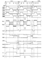
- FIG. 4 is a diagram showing source signal lines to which a voltage is applied in each horizontal period by the dot inversion driving method, and more specifically, FIG. 4A shows each color in the first horizontal period 1H (1).
- FIG. 4B is a diagram showing a source signal line in which a video signal is stored in a sub-pixel and then a reset voltage is applied.
- FIG. 4B shows a source signal line short-circuited at the beginning of the second horizontal period 1H (2).
- FIG. FIG. 5 is a diagram showing source signal lines to which a voltage is applied in each horizontal period by the dot inversion driving method. More specifically, FIG. 5A shows the second horizontal period 1H (2).
- FIG. 5 shows the second horizontal period 1H (2).
- FIG. 5B is a diagram showing source signal lines in which video signals are stored in sub-pixels of respective colors and then a reset voltage is applied, and FIG. 5B is a source signal short-circuited at the beginning of the third horizontal period 1H (3). It is a figure which shows a line.
- the dot inversion driving method in the first horizontal period 1H (1), positive red video signals and blue video signals are converted into source signal lines SLR1 to SLRm or source signal lines.
- the data is stored in one of the red subpixels and blue subpixels in the first row connected to any one of SLB1 to SLBm and the gate signal line GL1.
- the negative green video signal is stored in the first row of green subpixels connected to one of the source signal lines SLG1 to SLGm and the gate signal line GL1.
- the scanning signal applied to the gate signal line GL1 is changed from the high level to the low level, the positive reset voltage +5 V is applied to the source signal lines SLR1 to SLRm and the source signal lines SLB1 to SLBm, and the source signal lines SLG1 to A negative reset voltage of ⁇ 5 V is applied to SLGm.
- the voltages of the source signal lines SLR1 to SLRm and SLB1 to SLBm become + 5V, and the voltages of the source signal lines SLG1 to SLGm become ⁇ 5V.
- + 5V is the maximum voltage among the positive voltages corresponding to the video signal
- -5V is the minimum voltage (the absolute value is the maximum voltage) among the negative voltages corresponding to the video signal. .
- the negative red video signal and the blue video signal are connected to the source signal lines SLR1 to SLRm or the source signal lines SLB1 to SLBm and the gate signal line GL2.
- the positive green video signal is stored in the second row of green subpixels connected to one of the source signal lines SLG1 to SLGm and the gate signal line GL2.
- the scanning signal applied to the gate signal line GL2 is changed from the high level to the low level, + 5V is applied to the source signal lines SLG1 to SLGm, and ⁇ 5V is applied to the source signal lines SLR1 to SLRm and the source signal lines SLB1 to SLBm.
- the source signal lines SLG1 to SLGm have a voltage of + 5V
- the source signal lines SLR1 to SLRm and SLB1 to SLBm have a voltage of -5V.
- a video signal is supplied to the source signal line and stored in each sub-pixel every horizontal period up to the nth horizontal period 1H (n). Thereafter, + 5V or -5V is applied to each source signal line, and two of them are short-circuited. In this manner, the next video signal is repeatedly applied to the source signal lines SLR1 to SLBm that have reached 0V.
- the reset voltage is set to + 5V and ⁇ 5V which are the maximum and minimum values of the voltage according to the video signal.
- the reset voltage is not limited to this, and may be, for example, an intermediate voltage on the positive polarity side such as +3 V and -3 V and an intermediate voltage on the negative polarity side.
- a driver video amplifier for inverting the polarity of the reset voltage provided in the source driver 40 Power consumption can be reduced.
- the reset voltage may be a voltage whose absolute value is larger than the absolute value of the maximum value and the minimum value of the voltage corresponding to the video signal, for example, + 7V and ⁇ 7V.
- these voltages are used as the power source of the liquid crystal display device, they can be used as the reset voltage, so that it is not necessary to newly provide a circuit for generating the reset voltage. Thereby, the manufacturing cost of a liquid crystal display device can be reduced.
- the reset voltage is not only a positive voltage and a negative voltage, but it is necessary that their absolute values are equal as described above.
- the voltage of each source signal line is 0 V by charge redistribution described later. become.
- the above description regarding the reset voltage is applied not only to the liquid crystal display device according to the present embodiment, but also to the liquid crystal display devices according to second and third embodiments described later.
- the polarities of the voltages corresponding to the video signals of the respective colors applied to the respective source signal lines are shown in FIGS. 4A to 5B. And may have opposite polarities.
- FIG. 6 is a timing chart showing the operation of the liquid crystal display device. First, the first horizontal period 1H (1) will be described. As shown in FIG. 6, a high level matching instruction signal MA is simultaneously applied to all the discharge circuits 61 of the charge matching circuit 60 at time t1. As a result, all the discharge circuits 61 become conductive, and two source signal lines connected via the discharge circuit 61 are short-circuited by two. As a result, charge redistribution is performed between the shorted source signal lines, and the voltages of the source signal lines SLR1 to SLBm become 0V.
- high level selection signals ASWR1 to ASWRm are respectively applied to the selection circuits 50R1 to 50Rm connected to the source signal lines SLR1 to SLRm to which the display elements 15 functioning as red subpixels are connected.
- the selection circuits 50R1 to 50Rm become conductive, and the positive red video signals output from the source driver 40 to the video signal lines VSL1 to VSLm pass through the selection circuits 50R1 to 50Rm to the source signal lines SLR1 to SLRm. Given to each.
- the selection signals ASWR1 to ASWRm become low level, and at time t3, the gates of the selection circuits 50G1 to 50Gm connected to the source signal lines SLG1 to SLGm to which the display elements 15 functioning as green subpixels are connected are connected. High-level selection signals ASWG1 to ASWGm are respectively provided. As a result, the selection circuits 50G1 to 50Gm are turned on, and the negative green video signals output from the source driver 40 to the video signal lines VSL1 to VSLm are supplied to the source signal lines SLG1 to SLGm via the selection circuits 50G1 to 50Gm. Given to each.
- the selection signals ASWG1 to ASWGm go to a low level, and at time t4, the gates of the selection circuits 50B1 to 50Bm connected to the source signal lines SLB1 to SLBm to which the display elements 15 functioning as blue subpixels are connected are applied. High level selection signals ASWB1 to ASWBm are respectively provided. As a result, the selection circuits 50B1 to 50Bm are turned on, and the positive blue video signals output from the source driver 40 to the video signal lines VSL1 to VSLm are passed through the selection circuits 50B1 to 50Bm to the source signal lines SLB1 to SLBm. Given to each.
- the gate signal line GL1 is a period from when the voltage corresponding to the red video signal is applied to the source signal lines SLR1 to SLRm until the voltage corresponding to the blue video signal is applied to the source signal lines SLB1 to SLBm.
- a high-level scanning signal is applied to.
- a positive red video signal is applied to the pixel capacitor Cp of the red subpixel connected to the gate signal line GL1
- a negative green video signal is applied to the pixel capacitor Cp of the green subpixel.
- a positive blue video signal is applied to the pixel capacitor Cp of the sub-pixel.
- the scanning signal of the gate signal line GL1 is set to a low level.
- the TFT 11 of each subpixel is turned off, the red subpixel and the blue subpixel connected to the gate signal line GL1 store a positive video signal, and the green subpixel stores a negative video signal.
- the source signal lines SLR1 to SLRm and SLB1 to SLBm are given a positive video signal, and the source signal lines SLG1 to SLGm are given a negative video signal.
- the high level selection signals ASWG1 to ASWGm are simultaneously applied to the selection circuits 50G1 to 50Gm, respectively, in order to apply ⁇ 5V to the source signal lines SLG1 to SLGm to which the negative video signals are applied.
- the selection circuits 50G1 to 50Gm become conductive, and ⁇ 5V is applied to the source signal lines SLG1 to SLGm, respectively.
- the voltage of the source signal lines SLG1 to SLGm becomes ⁇ 5 V regardless of the voltage of the green video signal given at time t3.
- the high level selection signals ASWR1 to ASWRm and ASWB1 to ASWBm are selected by the selection circuit 50R1.
- the selection circuits 50R1 to 50Rm and 50B1 to 50Bm become conductive, and +5 V is applied to the source signal lines SLR1 to SLRm and SLB1 to SLBm, respectively.
- the voltages of the source signal lines SLR1 to SLRm and SLB1 to SLBm become + 5V regardless of the voltage of the red or blue video signal applied at time t2 or t4.
- a high-level matching instruction signal MA is simultaneously applied to the discharge circuit 61.
- all the discharge circuits 61 become conductive, and two source signal lines connected via the discharge circuit 61 are short-circuited by two.
- charge redistribution is performed between the shorted source signal lines, and the voltages of the source signal lines SLR1 to SLBm become 0V.
- a video signal obtained by inverting the polarity of the video signal applied in the first horizontal period 1H (1) is given to the source signal lines SLR1 to SLBm.
- a high-level scanning signal is applied to the gate signal line GL2 to activate it, the selection signals ASWR1 to ASWRm are set to high level, and negative red video is applied to the source signal lines SLR1 to SLRm.
- the selection signals ASWG1 to ASWGm are set to a high level, and positive green video signals are given to the source signal lines SLG1 to SLGm.
- the selection signals ASWB1 to ASWBm are set to a high level, and negative blue video signals are supplied to the source signal lines SLB1 to SLBm. Thereafter, the scanning signal applied to the gate signal line GL2 is set to the low level. As a result, the TFT 11 of each subpixel is turned off, the red subpixel and the blue subpixel connected to the gate signal line GL2 store a negative video signal, and the green subpixel stores a positive video signal. To do.
- the source signal lines SLR1 to SLRm and SLB1 to SLBm are given a negative video signal, and the source signal lines SLG1 to SLGm are given a positive video signal.
- the high level selection signals ASWG1 to ASWGm are simultaneously applied to the corresponding selection circuits 50G1 to 50Gm, respectively.
- the selection circuits 50G1 to 50Gm become conductive, and +5 V is applied to the source signal lines SLG1 to SLGm.
- the voltage of the source signal lines SLG1 to SLGm becomes + 5V regardless of the voltage of the green video signal given at time t9.
- the high level selection signals ASWR1 to ASWRm and ASWB1 to ASWBm are applied at time t12.
- the signals are simultaneously applied to the selection circuits 50R1 to 50Rm and 50B1 to 50Bm, respectively.
- the selection circuits 50R1 to 50Rm and 50B1 to 50Bm become conductive, and ⁇ 5V is applied to the source signal lines SLR1 to SLRm and SLB1 to SLBm.
- the voltages of the source signal lines SLR1 to SLRm and SLB1 to SLBm become ⁇ 5V regardless of the voltage of the red or blue video signal applied at time t8 or t10.
- high level matching instruction signal MA is simultaneously applied to discharge circuit 61.
- all the discharge circuits 61 become conductive, and two source signal lines connected via the discharge circuit 61 are short-circuited by two.
- charge redistribution is performed between the shorted source signal lines, and the voltages of the source signal lines SLR1 to SLBm become 0V.
- the next video signal is applied to the source signal lines SLR1 to SLBm whose voltages have become 0V.
- the reset voltage is a voltage having the same absolute value and different polarity, such as + 5V and -5V.
- voltages having the same absolute value and different polarities are, for example, + 5.1V and -5.2V, and if the source signal line is short-circuited, those voltages are close to 0V. It also includes a voltage that has substantially the same effect as the form. The same applies to the liquid crystal display devices according to second and third embodiments described later.
- the source signal line to which +5 V is applied and the source signal line to which ⁇ 5 V is applied are short-circuited, whereby charge is regenerated between the source signal lines. Distribution takes place and their voltage is 0V.
- the voltage of the source signal line is affected by the video signal applied in the immediately preceding one horizontal period.
- the voltage corresponds to the video signal. Therefore, such a liquid crystal display device can display a color image with little display unevenness and high uniformity.
- the selection circuits 50R1 to 50Bm analog switches with low power consumption during driving and high current driving capability are used. As a result, even if there are variations in characteristics of the thin film transistors constituting the analog switch, the source signal lines SLR1 to SLBm can be charged in a short time, so that display unevenness due to insufficient charging of the source signal lines SLR1 to SLBm can be reduced. it can.
- the discharge circuit 61 may be arranged so as to connect two adjacent source signal lines, the liquid crystal display device can be easily designed.
- Second Embodiment> ⁇ 2.1 Configuration of liquid crystal display device>
- the configuration of the liquid crystal display device according to the second embodiment of the present invention is the same as the configuration of the liquid crystal display device according to the first embodiment shown in FIG. Note that the liquid crystal display device according to this embodiment is driven by column inversion, unlike the liquid crystal display device of FIG.
- FIG. 7 is a diagram showing a configuration of the display unit 10 including the multiplexer 50 and the charge matching circuit 65 included in the liquid crystal display device according to the present embodiment. Since the configuration of the multiplexer 50 shown in FIG. 7 is the same as the configuration of the multiplexer 50 shown in FIG. 3, the same reference numerals as those in FIG.
- the charge matching circuit 65 also includes 3 m / 2 discharge circuits 66 formed of analog switches.
- the gate terminal of the N-channel TFT is directly connected to the display control circuit 20, and the gate terminal of the P-channel TFT is connected to the display control circuit 20 via an inverter. If the high-level matching instruction signal MA is given from the display control circuit 20 to the discharge circuit 66, both the N-channel and P-channel TFTs are turned on. As a result, all the discharge circuits 61 become conductive.
- the drain terminal of each TFT is connected to one source signal line of two source signal lines that give the same color video signal in adjacent pixels, and the source terminal is connected to the other source signal line. Yes.
- + 5V is applied to the source signal line SLR1 to which the positive red video signal is applied, and the source signal line SLR2 to which the negative red video signal is applied.
- -5V is applied to. Since the source signal line SLR1 and the source signal line SLR2 are connected via the discharge circuit 66, when the high level matching instruction signal MA is given to the discharge circuit 66 from the display control circuit 20, all the discharge circuits 66 are The conductive state is established, and the source signal line SLR1 and the source signal line SLR2 are short-circuited. As a result, the voltages of the source signal line SLR1 and the source signal line SLR2 are both 0V.
- a source signal line SLG1 and a source signal line SLG2 to which a green video signal is applied, and a source signal line SLB1 and a source signal line SLB2 to which a blue video signal is applied are connected via a discharge circuit 66, respectively. Yes. Therefore, when the high level matching instruction signal MA is applied, all the discharge circuits 66 are turned on. As a result, the source signal line SLG1 and the source signal line SLG2, and the source signal line SLB1 and the source signal line SLB2 are short-circuited, and their voltages are all 0V. In this way, the voltages of the source signal lines SLR1 to SLBm all become 0V.
- the polarity of the reset voltage applied to each of the source signal lines SLR1 to SLBm is the same as that in the first horizontal period 1H (1). Therefore, as in the case of the first horizontal period 1H (1), the voltages of the source signal lines SLR1 to SLBm become 0V for each horizontal period.
- FIG. 8 is a diagram showing source signal lines to which a voltage is applied in each horizontal period by the column inversion driving method. More specifically, FIG. 8A shows each color in the second horizontal period 1H (2).
- FIG. 8B is a diagram showing source signal lines in which video signals are stored in the sub-pixels of FIG. 8B and then a reset voltage is applied, and FIG. 8B is a source signal line short-circuited at the beginning of the third horizontal period 1H (3).
- FIG. 8 is a diagram showing source signal lines to which a voltage
- either of the source signal lines SLR1 to SLRm or the source signal lines SLB1 to SLBm to which the positive red video signal and the blue video signal are given, and the gate signal line GL2 Are stored in the red sub-pixel or blue sub-pixel in the second row connected to.
- a negative green video signal is stored in the second row of green sub-pixels connected to any of the supplied source signal lines SLG1 to SLGm and the gate signal line GL2.
- + 5V is applied to the source signal lines SLR1 to SLRm and the source signal lines SLB1 to SLBm
- ⁇ 5V is applied to the source signal lines SLG1 to SLGm.
- the video signals having the same polarity are stored in the sub-pixels of each color given the video signal to the source signal line. Thereafter, + 5V or -5V is applied to each source signal line, and two of them are short-circuited. In this way, the application of the next video signal to the source signal line at 0 V is repeated.
- FIG. 9 is a timing chart showing the operation of the liquid crystal display device according to the present embodiment. As shown in FIG. 9, the level of each signal in the first horizontal period 1H (1) is the same as the level of each signal in the timing chart shown in FIG. For this reason, the first horizontal period 1H (1) will be briefly described.
- the red subpixel and the blue subpixel connected to the gate signal line GL1 store a positive video signal, and the green subpixel stores a negative video signal. Further, + 5V is applied to the source signal lines SLR1 to SLRm and SLB1 to SLBm, and ⁇ 5V is applied to the source signal lines SLG1 to SLGm.
- the second horizontal period 1H (2) will be described.
- the high-level matching instruction signal MA is simultaneously applied to all the discharge circuits 66 of the charge matching circuit 65.
- all the discharge circuits 66 become conductive, and two source signal lines connected via the discharge circuit 66 are short-circuited by two.
- charge redistribution is performed between the two shorted source signal lines, and the voltages of the source signal lines SLR1 to SLBm become 0V.
- high-level selection signals ASWR1 to ASWRm are applied to the selection circuits 50R1 to 50Rm connected to the source signal lines SLR1 to SLRm to which the display elements functioning as red subpixels are connected, respectively.
- the selection circuits 50R1 to 50Rm become conductive, and the positive red video signals output from the source driver 40 to the video signal lines VSL1 to VSLm pass through the selection circuits 50R1 to 50Rm to the source signal lines SLR1 to SLRm.
- the selection signals ASWR1 to ASWRm go to the low level, and at time t9, the selection circuits 50G1 to 50Gm connected to the source signal lines SLG1 to SLGm connected to the display elements that function as the green subpixel are selected to the high level. Signals ASWG1 to ASWGm are respectively provided. As a result, the selection circuits 50G1 to 50Gm are turned on, and the negative green video signals output from the source driver 40 to the video signal lines VSL1 to VSLm are supplied to the source signal lines SLG1 to SLGm via the selection circuits 50G1 to 50Gm. Given to each.
- the selection signals ASWG1 and ASWG2 are set to the low level, and at time t10, the selection circuits 50B1 to 50Bm connected to the source signal lines SLB1 to SLBm connected to the display elements functioning as the blue subpixels are respectively set to the high level. Selection signals ASWB1 to ASWBm are applied. As a result, the selection circuits 50B1 to 50Bm are turned on, and the positive blue video signals output from the source driver 40 to the video signal lines VSL1 to VSLm are passed through the selection circuits 50B1 to 50Bm to the source signal lines SLB1 to SLBm. Given to each.
- the gate signal line GL2 has a period from when a voltage corresponding to the red video signal is applied to the source signal lines SLR1 to SLRm until a voltage corresponding to the blue video signal is applied to the source signal line SLBm.
- a high level scanning signal is applied.
- a positive red video signal is applied to the pixel capacitance Cp of the red subpixel connected to the gate signal line GL2, and a negative green video signal is applied to the pixel capacitance Cp of the green subpixel.
- a positive blue video signal is applied to the pixel capacitor Cp of the sub-pixel.
- the scanning signal of the gate signal line GL2 is set to the low level.
- the TFT 11 of each subpixel is turned off, the red subpixel and the blue subpixel connected to the gate signal line GL2 store a positive video signal, and the green subpixel stores a negative video signal.
- the source signal lines SLR1 to SLRm and SLB1 to SLBm are given a positive video signal, and the source signal lines SLG1 to SLGm are given a negative video signal.
- the high level selection signals ASWG1 to ASWGm are simultaneously applied to the selection circuits 50G1 to 50Gm, respectively.
- the selection circuits 50G1 to 50Gm become conductive, and ⁇ 5V is applied to the source signal lines SLG1 to SLGm.
- the voltage of the source signal lines SLG1 to SLGm becomes ⁇ 5 V regardless of the voltage of the green video signal given at time t9.
- the high level selection signals ASWR1 to ASWR1 and ASWB1 to ASWBm are selected by the selection circuits 50R1 to 50Rm and 50B1. ⁇ 50 Bm at the same time.
- the selection circuits 50R1 to 50Rm and 50B1 to 50Bm become conductive, and +5 V is applied to the source signal lines SLR1 to SLRm and SLB1 to SLBm.
- the voltages of the source signal lines SLR1 to SLRm and SLB1 to SLBm become + 5V regardless of the voltage of the red or blue video signal applied at time t8 or time t10.
- high-level matching instruction signal MA is applied to discharge circuit 66 at the same time. Thereby, all the discharge circuits 66 are made conductive, and the two source signal lines connected by the discharge circuit 66 are short-circuited. As a result, charge redistribution is performed between the shorted source signal lines, and the voltages of the source signal lines SLR1 to SLBm become 0V. In this way, the next video signal is applied to the source signal lines SLR1 to SLBm whose voltages have become 0V.
- the source signal lines are short-circuited two by two, whereby charge redistribution is performed between the source signal lines, and their voltage becomes 0V.
- the voltage of the source signal line is affected by the video signal applied in the immediately preceding one horizontal period.
- the voltage corresponds to the video signal. Therefore, such a liquid crystal display device can display a color image with little display unevenness and high uniformity.
- a liquid crystal display device driven by column inversion can be used as a monochromatic display device that displays only red video, for example.
- a reset voltage having the same polarity as the voltage corresponding to the video signal is alternately applied only to the source signal lines SLR1 to SLRm to which the video signal representing red is applied, and charge redistribution is performed between them.
- video signals are not applied to the source signal lines SLG1 to SLGm and SLB1 to SLBm. Therefore, it is not necessary to apply a reset voltage to the source signal lines SLG1 to SLGm and SLB1 to SLBm and perform charge redistribution between them.
- the charge redistribution is performed only between the source signal lines SLR1 to SLRm, so that the charge redistribution can be performed efficiently.
- the liquid crystal display device according to the present embodiment is a display device that is driven by dot inversion similarly to the liquid crystal display device according to the first embodiment, a diagram showing dot inversion driving and description thereof are omitted.
- FIG. 10 is a timing chart showing the operation of the liquid crystal display device according to the present embodiment.
- a high level matching instruction signal MA is given from the display control circuit 20 to the charge matching circuit 60 at time t1.
- all the discharge circuits 61 of the charge matching circuit 60 are turned on, and two source signal lines connected via the discharge circuit 61 are short-circuited two by two.
- charge redistribution is performed between the shorted source signal lines, and the voltages of the source signal lines SLR1 to SLBm become 0V.
- a positive video signal is applied to the red subpixel and the blue subpixel, and a negative video signal is applied to the green subpixel. Further, positive red video signals are supplied to the source signal lines SLR1 to SLRm, negative green video signals are supplied to the source signal lines SLG1 to SLGm, and positive blue video signals are supplied to the source signal lines SLB1 to SLBm, respectively. Applied.
- the high level selection signals ASWG1 to ASWGm are simultaneously applied to the corresponding selection circuits 50G1 to 50Gm, respectively. give.
- the selection circuits 50G1 to 50Gm become conductive, and ⁇ 5V is applied to the source signal lines SLG1 to SLGm.
- the voltage of the source signal lines SLG1 to SLGm becomes ⁇ 5 V regardless of the voltage of the green video signal given at time t3.
- the time for applying ⁇ 5V to the source signal lines SLG1 to SLGm is set to the same time as that for applying ⁇ 5V to the source signal lines SLG1 to SLGm at time t5 in FIG.
- the high level selection signals ASWR1 to ASWRm and ASWB1 to ASWBm are selected correspondingly.
- the signals are simultaneously applied to the circuits 50R1 to 50Rm and 50B1 to 50Bm, respectively.
- the selection circuits 50R1 to 50Rm and 50B1 to 50Bm become conductive, and +5 V is applied to the source signal lines SLR1 to SLRm and SLB1 to SLBm.
- the voltages of the source signal lines SLR1 to SLRm and SLB1 to SLBm become + 5V regardless of the voltage of the red or blue video signal applied at time t2 or t4.
- the time for applying + 5V to the source signal lines SLR1 to SLRm and SLB1 to SLBm is set to approximately twice the time for applying ⁇ 5V to the source signal lines SLG1 to SLGm at time t5.
- the second horizontal period 1H (2) will be described.
- the high-level matching instruction signal MA is simultaneously applied to all the discharge circuits 61 of the charge matching circuit 60.
- all the discharge circuits 61 become conductive, and two source signal lines connected via the discharge circuit 61 are short-circuited by two.
- charge redistribution is performed between the shorted source signal lines, and the voltages of the source signal lines SLR1 to SLBm become 0V.
- a negative video signal image is applied to the red subpixel and the blue subpixel, and a positive video signal is applied to the green subpixel.
- negative red video signals are supplied to the source signal lines SLR1 to SLRm
- positive green video signals are supplied to the source signal lines SLG1 to SLGm
- negative blue video signals are supplied to the source signal lines SLB1 to SLBm, respectively.
- high level selection signals ASWG1 to ASWGm are simultaneously applied to the selection circuits 50G1 to 50Gm in order to apply +5 V to the source signal lines SLG1 to SLGm to which the positive video signals are applied.
- the selection circuits 50G1 to 50Gm become conductive, and +5 V is applied to the source signal lines SLG1 to SLGm.
- the time for applying + 5V to the source signal lines SLG1 to SLGm is set to the same time as that for applying ⁇ 5V to the source signal lines SLG1 to SLGm at time t11 in FIG.
- the high level selection signals ASWR1 to ASWRm and ASWB1 to ASWBm are selected.
- 50R1 to 50Rm and 50B1 to 50Bm are respectively given simultaneously.
- the selection circuits 50R1 to 50Rm and 50B1 to 50Bm become conductive, and ⁇ 5V is applied to the source signal lines SLR1 to SLRm and SLB1 to SLBm.
- the voltages of the source signal lines SLR1 to SLRm and SLB1 to SLBm become ⁇ 5V regardless of the voltage of the red or blue video signal applied at time t8 or t10.
- the time for applying ⁇ 5V to the source signal lines SLR1 to SLRm and SLB1 to SLBm is set to approximately twice the time for applying + 5V to the source signal lines SLG1 to SLGm at time t11.
- a high-level matching instruction signal MA is simultaneously applied to all the discharge circuits 61 of the charge matching circuit 60.
- all the discharge circuits 61 become conductive, and two source signal lines connected to the discharge circuit 61 are short-circuited by two.
- charge redistribution is performed between the shorted source signal lines, and the voltages of the source signal lines SLR1 to SLBm become 0V.
- the next video signal is applied to the source signal lines SLR1 to SLBm whose voltages have become 0V.
- the reason why the time for applying the reset voltage to the source signal lines SLR1 to SLRm and the source signal lines SLB1 to SLBm is set longer than the time for applying the reset voltage to the source signal lines SLG1 to SLGm will be described.
- the selection signal ASWG1 is supplied to the selection circuit 50G1
- the source signal line SLG1 is connected to the video signal line VSL1
- the source signal line SLG1 is charged to ⁇ 5V.
- selection signals ASWR1 and ASWB1 are supplied to the selection circuits 50R1 and 50B1, respectively, and the source signal lines SLR1 and SLB1 are simultaneously connected to the video signal line VSL1, I have to charge it.
- the charging time of the two source signal lines SLR1 and SLB1 connected to the video signal line VSL1 is the same as the charging time of the one source signal line SLG1, the source signal line SLR1 to be charged to + 5V.
- the charging time ends before the voltage of SLB1 becomes + 5V, and the source signal lines SLR1 and SLB1 may be charged only to a voltage lower than + 5V. In this case, even if the source signal line SLG1 charged to ⁇ 5V and the source signal line SLR1 charged only to a voltage lower than + 5V are short-circuited, those voltages do not become 0V.
- the time for charging the source signal lines SLR1 and SLB1 connected to the video signal line VSL1 to + 5V is set to be approximately twice the time for charging the source signal line SLG1 to -5V, so that each source The signal lines SLR1 and SLB1 are reliably charged to + 5V, respectively.
- the source signal line SLR1 and the source signal line SLG1 are short-circuited, their voltages become 0V.
- the time for charging the source signal lines SLR1 and SLB1 connected to the video signal line VSL1 to + 5V is not twice the time for charging the source signal line SLG1 to -5V, but approximately twice. It was.
- the reason why it is approximately double is that charging is completed in a short time if the current value for charging the source signal lines SLR1 and SLB1 is large, and on the contrary, if the current value is small, it takes a long time. This is because even if the number of source signal lines is doubled, it is not always necessary to double the time.
- the time for charging the source signal lines SLR1 to SLRm and SLB1 to SLBm connected to the video signal lines VSL1 to VSLm to + 5V or ⁇ 5V is set.
- the voltage of the source signal lines SLR1 to SLB1 can be reliably charged to + 5V or ⁇ 5V by setting the source signal lines SLG1 to SLGm to approximately twice the time for charging to ⁇ 5V or + 5V. If the source signal lines charged in this way are short-circuited, their voltages are surely 0V. As a result, since a voltage corresponding to the next video signal is applied to the source signal line at 0 V, a color image with less display unevenness and higher uniformity can be displayed.
- the time for applying + 5V or ⁇ 5V to the source signal lines SLR1 to SLRm and SLB1 to SLBm is set to the source signal lines SLG1 to SLBm.
- the time during which + 5V or ⁇ 5V is applied to the source signal lines SLR1 to SLRm and SLB1 to SLBm is set to the source signal lines SLG1 to SLGm ⁇ You may make it longer than the time which applies 5V or + 5V. In this case, the same effect as in the case of the present embodiment can be obtained.
- the number of source signal lines to which +5 V is applied is twice the number of source signal lines to which ⁇ 5 V is applied, but is not limited to two times, and may be three times or more, or It may be less than half.
- the time for applying + 5V or ⁇ 5V depending on the number of source signal lines all the source signal lines can be charged until the reset voltage is reached.
- FIG. 11 is a diagram illustrating a configuration of the display unit 10 including the charge matching circuit 60 in the first modification of the liquid crystal display device according to the first embodiment.
- Each component shown in FIG. 11 is given the same reference numeral as the component shown in FIG. 3 or a corresponding reference symbol.
- the liquid crystal display device according to the first embodiment is a liquid crystal display device that can display a color image
- the present invention is also applicable to a liquid crystal display device that cannot display a color image.
- the video signal output from the source driver does not include the video signal of each color
- the video signals and + 5V and ⁇ 5V output from the source driver are directly applied to the source signal lines SL1 to SL.
- the liquid crystal display device according to the present modification can also display an image with little display unevenness and high uniformity.
- liquid crystal display device can display an image with little display unevenness and high uniformity by adopting the same configuration as that of the first modification.
- FIG. 12 is a diagram illustrating a configuration of the display unit 10 including the charge matching circuit 60 in the second modification of the liquid crystal display device according to the first embodiment.
- Each component shown in FIG. 11 is given the same reference numeral as the component shown in FIG. 3 or a corresponding reference symbol.
- the discharge circuit 61 is short-circuited for every two adjacent source signal lines, but the discharge circuit 61 is used for every four adjacent source signal lines. You may short-circuit.
- + 5V is applied to the two source signal lines
- ⁇ 5V is applied to the other two source signal lines. Therefore, these four source signal lines are connected by the discharge circuit 61, and the discharge circuit 61 is brought into conduction to short-circuit them.
- the voltages of the source signal lines SLR1 to SLBm can be set to 0V.
- the liquid crystal display device according to the present modification can also display an image with little display unevenness and high uniformity.
- the number of source signal lines connected by the discharge circuit 61 is not limited to two or four as long as the number of source signal lines to which + 5V is applied is equal to the number of source signal lines to which ⁇ 5V is applied.
- the liquid crystal display device according to the second embodiment can display an image with little display unevenness and high uniformity by adopting the same configuration as that of the first modification.
- the liquid crystal display device has been described as an example.
- the present invention is not limited to this, and can be applied to an organic EL (Electro Luminescence) display device or the like.
- the present invention is applied to a matrix display device such as an active matrix liquid crystal display device, and is particularly suitable for a display device that performs charge redistribution.
- SYMBOLS 10 Display part 15 ... Display element 30 ... Gate driver (scanning signal line drive circuit) 40 ... Source driver (data signal line drive circuit) 50 ... Multiplexer 50R1-50Bm ... Selection circuit 60, 65 ... Charge matching circuit 61, 66 ... Discharge circuit VSL1-VSLm ... Video signal line SLR1-SLBm ... Source signal line (sub data signal line) SL1 to SLm ... Source signal line (data signal line) GL1 to GLn: Gate signal lines (scanning signal lines) ASWR1 to ASWBm ... selection signal MA ... matching signal
Landscapes
- Engineering & Computer Science (AREA)
- Chemical & Material Sciences (AREA)
- Crystallography & Structural Chemistry (AREA)
- Physics & Mathematics (AREA)
- Computer Hardware Design (AREA)
- General Physics & Mathematics (AREA)
- Theoretical Computer Science (AREA)
- Control Of Indicators Other Than Cathode Ray Tubes (AREA)
- Liquid Crystal Display Device Control (AREA)
Abstract
Description
本発明は、表示装置およびその駆動方法に関し、特に、電荷再分配(チャージシェア)を行なう表示装置およびその駆動方法に関する。 The present invention relates to a display device and a driving method thereof, and more particularly to a display device that performs charge redistribution (charge sharing) and a driving method thereof.
近年、表示部の高精細化、大型化が進展し、表示部に表示される映像の品位に影響を及ぼす駆動時のノイズが問題になっている。このようなノイズを低減するために、液晶表示装置では、各画素の対向電極に直流電圧を印加し、ソース信号線ごとに、正極性の映像信号と負極性の映像信号とを交互に与えるドット反転駆動またはカラム反転駆動を行なうことによって、映像の表示品位を向上させている。 In recent years, high-definition and large-sized display units have progressed, and driving noise that affects the quality of images displayed on the display unit has become a problem. In order to reduce such noise, in a liquid crystal display device, a dot voltage is applied to a counter electrode of each pixel to alternately apply a positive video signal and a negative video signal for each source signal line. Image display quality is improved by performing inversion driving or column inversion driving.
しかし、フレーム期間ごとに、ソース信号線に与える映像信号の極性を反転させる必要があり、特にドット反転駆動ではさらに1水平期間(1H)ごとにも映像信号の極性を反転させる必要がある。このように映像信号の極性を反転させる場合、その都度ドライバビデオアンプの極性を切り替えて映像信号のスイング幅を大きくしなければならないので、消費電力が大きくなる。 However, it is necessary to invert the polarity of the video signal applied to the source signal line for each frame period. In particular, in the case of dot inversion driving, it is necessary to invert the polarity of the video signal every horizontal period (1H). When the polarity of the video signal is inverted in this way, the polarity of the driver video amplifier must be switched each time to increase the swing width of the video signal, resulting in an increase in power consumption.
そこで、例えば特許文献1および2に記載されているように、隣接する2本のソース信号線ごとに放電回路を設け、1水平期間ごとに放電回路を同時に導通させる。このとき、一方のソース信号線に正極性の映像信号が与えられ、他方のソース信号線に負極性の映像信号があたえられているので、それらを導通させることによって、隣接するソース信号線間で電荷再分配が行なわれる。電荷再分配によって、映像信号の極性を反転させる際に必要な映像信号のスイング幅が小さくなるので、消費電力が低減される。
Therefore, for example, as described in
しかし、各ソース信号線に印加される映像信号に応じた電圧は映像信号ごとに異なるので、隣接する2本のソース信号線の電荷再分配を行なった後のソース信号線の電圧はその都度異なる。すなわち、電荷再分配後のソース信号線の電圧が、0Vになったり、正電圧になったり、負電圧になったりする。このようなソース信号線に、次の映像信号を与えても、ソース信号線の電圧は電荷再分配後の電圧の影響を受け、与えられた映像信号の電圧よりも高くなったり、低くなったりする場合がある。このような場合、表示部に表示される映像の均一性が損なわれるという問題がある。 However, since the voltage corresponding to the video signal applied to each source signal line is different for each video signal, the voltage of the source signal line after charge redistribution between two adjacent source signal lines is different each time. . That is, the voltage of the source signal line after charge redistribution becomes 0V, a positive voltage, or a negative voltage. Even if the next video signal is applied to such a source signal line, the voltage of the source signal line is affected by the voltage after charge redistribution and may be higher or lower than the voltage of the applied video signal. There is a case. In such a case, there is a problem that the uniformity of the image displayed on the display unit is impaired.
そこで、本発明は、電荷再分配後に表示される映像の均一性が損なわれない表示装置およびその駆動方法を提供することを目的とする。 Therefore, an object of the present invention is to provide a display device in which the uniformity of an image displayed after charge redistribution is not impaired, and a driving method thereof.
本発明の第1の局面は、アクティブマトリクス型の表示装置であって、
複数のデータ信号線と、前記複数のデータ信号線と交差する複数の走査信号線と、前記複数のデータ信号線と前記複数の走査信号線との交差点にそれぞれ対応してマトリクス状に配置された複数の画素とを有する表示部と、
前記複数の走査信号線を順に選択して活性化する走査信号線駆動回路と、
正極性の電圧と負極性の電圧とをデータ信号線ごとに交互に印加するデータ信号線駆動回路と、
正極性の電圧が印加された前記データ信号線と、負極性の電圧が印加された前記データ信号線とを同じ本数ずつ接続する複数の放電回路とを備え、
前記データ信号線駆動回路は、映像信号に応じた正極性の電圧と負極性の電圧とを前記データ信号線ごとに交互に印加し、次に絶対値が等しくかつ極性が前記映像信号に応じた電圧と同じ第1リセット電圧を前記データ信号線にそれぞれ印加し、
前記放電回路は、1水平期間ごとに、前記第1リセット電圧が前記データ信号線に印加された後に、前記放電回路に接続された前記データ信号線ごとに短絡させることを特徴とする。
A first aspect of the present invention is an active matrix display device,
The plurality of data signal lines, the plurality of scanning signal lines intersecting with the plurality of data signal lines, and the intersections of the plurality of data signal lines and the plurality of scanning signal lines are arranged in a matrix. A display unit having a plurality of pixels;
A scanning signal line driving circuit for sequentially selecting and activating the plurality of scanning signal lines;
A data signal line driving circuit for alternately applying a positive voltage and a negative voltage for each data signal line;
A plurality of discharge circuits that connect the same number of data signal lines to which a positive voltage is applied and the data signal lines to which a negative voltage is applied;
The data signal line driving circuit alternately applies a positive voltage and a negative voltage corresponding to the video signal for each data signal line, and then the absolute value is equal and the polarity corresponds to the video signal. A first reset voltage equal to the voltage is applied to each of the data signal lines;
The discharge circuit may be short-circuited for each data signal line connected to the discharge circuit after the first reset voltage is applied to the data signal line every horizontal period.
本発明の第2の局面は、本発明の第1の局面において、
複数色の映像をそれぞれ表わす複数の色映像信号を含む前記映像信号を色映像信号ごとに分割する選択回路をさらに備え、
前記表示部に配置された前記画素は前記複数の色映像信号にそれぞれ対応する複数の副画素からなり、
前記データ信号線は、前記複数の色映像信号を時分割して出力する映像信号線と、前記複数の副画素にそれぞれ接続された複数の副データ信号線とからなり、
前記選択回路は前記複数の色映像信号に応じた電圧を前記複数の副データ信号線にそれぞれ与え、
前記放電回路は、正極性の電圧を印加された副データ信号線と、負極性の電圧を印加された副データ信号線とを同じ本数ずつ接続し、
前記データ信号線駆動回路は、前記色映像信号に応じた正極性の電圧と負極性の電圧とを前記副データ信号線ごとに交互に印加し、次に絶対値が等しくかつ極性が前記色映像信号に応じた電圧と同じ第2リセット電圧を前記副データ信号線にそれぞれ印加し、
前記放電回路は、1水平期間ごとに、前記第2リセット電圧が前記副データ信号線に印加された後に、前記放電回路に接続された前記副データ信号線ごとに短絡させることを特徴とする。
According to a second aspect of the present invention, in the first aspect of the present invention,
A selection circuit for dividing the video signal including a plurality of color video signals each representing a plurality of colors of video into each color video signal;
The pixels arranged in the display unit include a plurality of sub-pixels corresponding to the plurality of color video signals,
The data signal line includes a video signal line for time-dividing and outputting the plurality of color video signals, and a plurality of sub data signal lines respectively connected to the plurality of sub pixels.
The selection circuit applies voltages corresponding to the plurality of color video signals to the plurality of sub data signal lines, respectively.
The discharge circuit connects the same number of sub data signal lines to which a positive voltage is applied and sub data signal lines to which a negative voltage is applied,
The data signal line driving circuit alternately applies a positive voltage and a negative voltage corresponding to the color video signal for each sub data signal line, and then the absolute value is equal and the polarity is the color video. A second reset voltage that is the same as the voltage corresponding to the signal is applied to each of the sub data signal lines;
The discharge circuit may be short-circuited for each sub-data signal line connected to the discharge circuit after the second reset voltage is applied to the sub-data signal line every horizontal period.
本発明の第3の局面は、本発明の第2の局面において、
前記第2リセット電圧を前記副データ信号線に印加する時間は、前記映像信号線ごとに接続された前記副データ信号線の本数に応じて長くなることを特徴とする。
According to a third aspect of the present invention, in the second aspect of the present invention,
The time for applying the second reset voltage to the sub data signal line is longer according to the number of sub data signal lines connected to each video signal line.
本発明の第4の局面は、本発明の第2の局面において、第2の発明において、
前記第2リセット電圧の絶対値は、前記色映像信号に応じた最大電圧および最小電圧の絶対値以下であることを特徴とする。
According to a fourth aspect of the present invention, in the second aspect of the present invention,
The absolute value of the second reset voltage is less than or equal to the absolute value of the maximum voltage and the minimum voltage according to the color video signal.
本発明の第5の局面は、本発明の第2の局面において、
前記選択回路はアナログスイッチによって構成されていることを特徴とする。
According to a fifth aspect of the present invention, in the second aspect of the present invention,
The selection circuit is constituted by an analog switch.
本発明の第6の局面は、本発明の第2の局面において、
前記放電回路は、隣接する2本の前記副データ信号線を接続することを特徴とする。
According to a sixth aspect of the present invention, in the second aspect of the present invention,
The discharge circuit connects two adjacent sub data signal lines.
本発明の第7の局面は、本発明の第2の局面において、
前記放電回路は、同じ色の前記色映像信号を与えられた副データ信号線のうち、最も近い2本の前記副データ信号線を接続することを特徴とする。
According to a seventh aspect of the present invention, in the second aspect of the present invention,
The discharge circuit connects the two closest sub data signal lines among the sub data signal lines to which the color video signal of the same color is applied.
本発明の第8の局面は、本発明の第2の局面において、
前記画素は、赤色副画素、緑色副画素および青色副画素を含むことを特徴とする。
According to an eighth aspect of the present invention, in the second aspect of the present invention,
The pixel includes a red subpixel, a green subpixel, and a blue subpixel.
本発明の第9の局面は、本発明の第8の局面において、
前記赤色副画素に接続された前記副データ信号線および前記青色副画素に接続された前記副データ信号線と、前記緑色副画素に接続された前記副データ信号線とに、それぞれ異なる極性の前記第2リセット電圧が印加され、
前記赤色副画素に接続された前記副データ信号線と前記青色副画素に接続された前記副データ信号線とに前記第2リセット電圧を印加する時間は、前記緑色副画素に接続された前記副データ信号線に前記第2リセット電圧を印加する時間よりも長いことを特徴とする。
A ninth aspect of the present invention is the eighth aspect of the present invention,
The sub-data signal line connected to the red sub-pixel and the sub-data signal line connected to the blue sub-pixel and the sub-data signal line connected to the green sub-pixel have different polarities. A second reset voltage is applied;
The time for applying the second reset voltage to the sub-data signal line connected to the red sub-pixel and the sub-data signal line connected to the blue sub-pixel is the sub-data connected to the green sub-pixel. The time is longer than the time for applying the second reset voltage to the data signal line.
本発明の第10の局面は、本発明の第2の局面において、
前記データ信号線駆動回路はドット反転駆動を行なうことを特徴とする。
According to a tenth aspect of the present invention, in the second aspect of the present invention,
The data signal line driving circuit performs dot inversion driving.
本発明の第11の局面は、本発明の第2の局面において、
前記データ信号線駆動回路はカラム反転駆動を行なうことを特徴とする。
An eleventh aspect of the present invention is the second aspect of the present invention,
The data signal line driving circuit performs column inversion driving.
本発明の第12の局面は、複数のデータ信号線と、前記複数のデータ信号線と交差する複数の走査信号線と、前記複数のデータ信号線と前記複数の走査信号線との交差点にそれぞれ対応してマトリクス状に配置された複数の画素とを有する表示部と、
前記複数の走査信号線を順に選択して活性化する走査信号線駆動回路と、
正極性の電圧と負極性の電圧とをデータ信号線ごとに交互に印加するデータ信号線駆動回路と、
正極性の電圧が印加された前記データ信号線と、負極性の電圧が印加された前記データ信号線とを同じ本数ずつ接続する複数の放電回路とを備えた、アクティブマトリクス型の表示装置の駆動方法であって、
映像信号に応じた正極性の電圧と負極性の電圧とを前記データ信号線ごとに交互に印加する第1の電圧印加ステップと、
前記映像信号に応じた正極性の電圧と負極性の電圧とを印加した後に、絶対値が等しくかつ極性が前記映像信号に応じた電圧と同じ第1リセット電圧を前記データ信号線にそれぞれ印加する第2の電圧印加ステップと、
1水平期間ごとに、前記第1リセット電圧を印加した後に前記放電回路を導通させることにより、前記放電回路に接続された前記データ信号線ごとに短絡させる短絡ステップとを備えることを特徴とする。
According to a twelfth aspect of the present invention, a plurality of data signal lines, a plurality of scanning signal lines intersecting with the plurality of data signal lines, and intersections of the plurality of data signal lines and the plurality of scanning signal lines are respectively provided. A display unit having a plurality of pixels correspondingly arranged in a matrix;
A scanning signal line driving circuit for sequentially selecting and activating the plurality of scanning signal lines;
A data signal line driving circuit for alternately applying a positive voltage and a negative voltage for each data signal line;
Driving an active matrix display device comprising: the data signal line to which a positive voltage is applied; and a plurality of discharge circuits that connect the same number of data signal lines to which a negative voltage is applied. A method,
A first voltage application step of alternately applying a positive voltage and a negative voltage corresponding to the video signal for each data signal line;
After applying a positive voltage and a negative voltage corresponding to the video signal, a first reset voltage having the same absolute value and the same polarity as the voltage corresponding to the video signal is applied to the data signal line. A second voltage application step;
A short-circuiting step for short-circuiting each data signal line connected to the discharge circuit by conducting the discharge circuit after applying the first reset voltage every horizontal period.
本発明の第13の局面は、本発明の第12の局面において、
複数色の映像をそれぞれ表わす複数の色映像信号を含む前記映像信号を色映像信号ごとに分割する選択回路をさらに備え、
前記表示部に配置された前記画素は前記複数色にそれぞれ対応する複数の副画素からなり、
前記データ信号線は、前記複数の色映像信号を時分割して出力する映像信号線と、前記副画素にそれぞれ接続された複数の副データ信号線とからなり、
前記第1の電圧印加ステップは、前記複数の色映像信号に応じた正極性の電圧と負極性の電圧とを前記複数の副データ信号線ごとに交互に印加し、
前記第2の電圧印加ステップは、前記複数の色映像信号に応じた電圧を前記複数の副データ信号線にそれぞれ与えた後に、絶対値が等しくかつ極性が前記色映像信号に応じた電圧と同じ第2リセット電圧を前記副データ信号線にそれぞれ印加し、
前記短絡ステップは、1水平期間ごとに、前記第2リセット電圧を印加した後に、前記放電回路に接続された前記副データ信号線ごとに短絡させることを特徴とする。
A thirteenth aspect of the present invention is the twelfth aspect of the present invention,
A selection circuit for dividing the video signal including a plurality of color video signals each representing a plurality of colors of video into each color video signal;
The pixels arranged in the display unit include a plurality of sub-pixels corresponding to the plurality of colors,
The data signal line includes a video signal line for time-dividing and outputting the plurality of color video signals, and a plurality of sub data signal lines respectively connected to the sub-pixels.
In the first voltage application step, a positive voltage and a negative voltage corresponding to the plurality of color video signals are alternately applied to the plurality of sub data signal lines,
In the second voltage applying step, after applying voltages corresponding to the plurality of color video signals to the plurality of sub data signal lines, the absolute values are equal and the polarities are the same as the voltages corresponding to the color video signals. Applying a second reset voltage to each of the sub-data signal lines;
In the short-circuiting step, the second reset voltage is applied every horizontal period, and then the sub-data signal line connected to the discharge circuit is short-circuited.
本発明の第1および第12の局面によれば、1水平期間ごとに、映像信号に応じた正極性の電圧と負極性の電圧とをデータ信号線ごとに交互に印加する。次に、絶対値が等しくかつ極性が映像信号に応じた電圧と同じ第1リセット電圧をデータ信号線にそれぞれ印加する。これにより、映像信号線に応じた電圧ではなく、絶対値が等しくかつ極性が異なる第1リセット電圧がデータ信号線ごとに交互に印加される。この状態で、第1リセット電圧を印加されたデータ信号線を短絡させると、データ信号線間で電荷再分配が行なわれ、それらの電圧は0Vになる。このようなデータ信号線に次の1水平期間の映像信号に応じた電圧を印加した場合、データ信号線の電圧は直前の1水平期間に印加された映像信号の影響を受けない。このため、表示装置は、表示むらが少なく、均一性が高い映像を表示することができる。なお、絶対値が等しくかつ極性が異なる電圧には、ソース信号線を短絡させれば、それらの電圧は0Vに近い値になり、上記効果と実質的に同一の効果を奏するような電圧も含まれる。 According to the first and twelfth aspects of the present invention, a positive voltage and a negative voltage corresponding to the video signal are alternately applied to each data signal line every horizontal period. Next, a first reset voltage having the same absolute value and the same polarity as the voltage corresponding to the video signal is applied to each data signal line. As a result, instead of the voltage corresponding to the video signal line, the first reset voltage having the same absolute value and different polarity is alternately applied to each data signal line. In this state, when the data signal line to which the first reset voltage is applied is short-circuited, charge redistribution is performed between the data signal lines, and these voltages become 0V. When a voltage corresponding to the video signal in the next one horizontal period is applied to such a data signal line, the voltage of the data signal line is not affected by the video signal applied in the immediately preceding one horizontal period. For this reason, the display device can display an image with little display unevenness and high uniformity. It should be noted that voltages having the same absolute value and different polarities include voltages that have substantially the same effect as the above effect when the source signal lines are short-circuited, and those voltages become values close to 0V. It is.
本発明の第2および第13の局面によれば、1水平期間ごとに、色映像信号に応じた正極性の電圧と負極性の電圧とを副データ信号線ごとに交互に印加する。次に、絶対値が等しくかつ極性が色映像信号に応じた電圧と同じ第2リセット電圧を副データ信号線にそれぞれ印加する。これにより、色映像信号線に応じた電圧ではなく、絶対値が等しくかつ極性が異なる第2リセット電圧が副データ信号線ごとに交互に印加される。この状態で、第2リセット電圧を印加された副データ信号線を短絡させると、副データ信号線間で電荷再分配が行なわれ、それらの電圧は0Vになる。このような副データ信号線に次の1水平期間の色映像信号に応じた電圧を印加した場合、副データ信号線の電圧は直前の1水平期間に印加された色映像信号の影響を受けない。このため、表示装置は、表示むらが少なく、均一性が高いカラー映像を表示することができる。 According to the second and thirteenth aspects of the present invention, the positive voltage and the negative voltage corresponding to the color video signal are alternately applied to the sub-data signal lines every horizontal period. Next, a second reset voltage having the same absolute value and the same polarity as the voltage corresponding to the color video signal is applied to the sub data signal line. As a result, a second reset voltage having the same absolute value and different polarity is applied alternately to each sub data signal line, not the voltage corresponding to the color video signal line. In this state, when the sub data signal line to which the second reset voltage is applied is short-circuited, charge redistribution is performed between the sub data signal lines, and these voltages become 0V. When a voltage corresponding to the color video signal in the next one horizontal period is applied to such a sub data signal line, the voltage of the sub data signal line is not affected by the color video signal applied in the immediately preceding one horizontal period. . For this reason, the display device can display a color image with little display unevenness and high uniformity.
本発明の第3の局面によれば、第2リセット電圧は、1本の映像信号線から同じ極性ごとに1本または2本以上の副データ信号線に同時に印加される。そこで、第2リセット電圧を印加する副データ信号線の本数が多い場合には、それらの副データ信号線の電圧を第2リセット電圧まで同時に充電するための時間を長くする必要がある。このように、副データ信号線の本数に応じて充電時間を長くし、すべての副データ信号線の電圧を第2リセット電圧になるまで充電することにより、副データ信号線に充電された極性が異なる電圧の絶対値は等しくなる。次に、極性が異なる第2リセット電圧を充電された副データ信号線を短絡させ、それらの電圧を0Vにする。これにより、表示装置は、表示むらが少なく、均一性が高いカラー映像を表示することができる。 According to the third aspect of the present invention, the second reset voltage is simultaneously applied from one video signal line to one or more sub data signal lines with the same polarity. Therefore, when the number of sub data signal lines to which the second reset voltage is applied is large, it is necessary to lengthen the time for charging the voltages of these sub data signal lines to the second reset voltage at the same time. As described above, the charging time is lengthened according to the number of the sub data signal lines, and the voltages of all the sub data signal lines are charged until the second reset voltage is reached. The absolute values of the different voltages are equal. Next, the sub data signal lines charged with the second reset voltages having different polarities are short-circuited, and those voltages are set to 0V. Accordingly, the display device can display a color image with little display unevenness and high uniformity.
本発明の第4の局面によれば、第2リセット電圧の絶対値は、映像信号に応じた電圧の最大値および最小値の絶対値よりも小さいので、第2リセット電圧を生成する際のデータ信号線駆動回路の消費電力を低減することができる。 According to the fourth aspect of the present invention, since the absolute value of the second reset voltage is smaller than the absolute value of the maximum value and the minimum value of the voltage according to the video signal, data when generating the second reset voltage The power consumption of the signal line driver circuit can be reduced.
本発明の第5の局面によれば、アナログスイッチは、駆動時の消費電力が少なく、電流駆動能力が高いスイッチである。そこで、選択回路としてアナログスイッチを用いれば、アナログスイッチを構成する薄膜トランジスタの特性ばらつきがあっても、副データ信号線を短時間で充電できる。これにより、副データ信号線を短時間で第2リセット電圧まで充電できるので、副データ信号線の充電不足に起因する表示むらを少なくすることができる。 According to the fifth aspect of the present invention, the analog switch is a switch with low power consumption during driving and high current driving capability. Therefore, if an analog switch is used as the selection circuit, the sub data signal line can be charged in a short time even if the characteristics of the thin film transistors constituting the analog switch vary. As a result, the sub data signal line can be charged to the second reset voltage in a short time, so that display unevenness due to insufficient charging of the sub data signal line can be reduced.
本発明の第6の局面によれば、隣接する2本の副データ信号線を接続するように放電回路を配置すればよいので、表示装置の設計を容易に行なうことができる。 According to the sixth aspect of the present invention, since the discharge circuit may be arranged so as to connect two adjacent sub data signal lines, the display device can be easily designed.
本発明の第7の局面によれば、同じ色の色映像信号を与えられた副データ信号線のうち、最も近い2本の副データ信号線を放電回路によって接続した表示装置を、特定の色の映像のみを表示する単色表示させる表示装置として用いた場合に、次のような効果を奏する。すなわち、特定の色を表わす色映像信号を与えられた副データ信号線にのみ第2リセット電圧を印加し、他の副データ信号線には色映像信号を与えないようにするので、それらの副データ信号線には第2リセット電圧も印加されない。このような場合に、電荷再分配は、特定の色を表わす色映像信号を与えられた副データ信号線間のみで行なわれるので、電荷再分配を効率よく行なうことができる。 According to the seventh aspect of the present invention, a display device in which two closest sub data signal lines among sub data signal lines to which a color video signal of the same color is given is connected by a discharge circuit is connected to a specific color. When used as a display device for displaying only a single color, the following effects are obtained. That is, the second reset voltage is applied only to the sub-data signal line to which the color video signal representing a specific color is applied, and the color video signal is not applied to the other sub-data signal lines. The second reset voltage is not applied to the data signal line. In such a case, charge redistribution is performed only between sub-data signal lines to which a color video signal representing a specific color is applied, so that charge redistribution can be performed efficiently.
本発明の第8の局面によれば、画素は、赤色副画素、緑色副画素および青色副画素を含むので、表示装置はカラー映像を表示することができる。 According to the eighth aspect of the present invention, since the pixel includes a red subpixel, a green subpixel, and a blue subpixel, the display device can display a color image.
本発明の第9の局面によれば、赤色副画素および青色副画素に接続された副データ信号線に第2リセット電圧を同時に印加する時間を、緑色副画素に接続された副データ信号線に第2リセット電圧を印加する時間よりも長くする。これにより、すべての副データ信号線の電圧を第2リセット電圧になるまで充電することができる。次に、極性が異なる第2リセット電圧を充電された副データ信号線を短絡させ、それらの電圧を0Vにする。これにより、表示装置は、表示むらが少なく、均一性が高いカラー映像を表示することができる。 According to the ninth aspect of the present invention, the time for simultaneously applying the second reset voltage to the sub-data signal lines connected to the red sub-pixel and the blue sub-pixel is set to the sub-data signal line connected to the green sub-pixel. The time is longer than the time for applying the second reset voltage. Thereby, it is possible to charge all the sub data signal lines until the second reset voltage is reached. Next, the sub data signal lines charged with the second reset voltages having different polarities are short-circuited, and those voltages are set to 0V. Accordingly, the display device can display a color image with little display unevenness and high uniformity.
本発明の第10の局面によれば、ドット反転駆動を行なうデータ信号線駆動回路を備えた表示装置は、極性が異なる第2リセット電圧を印加された副データ信号線を短絡させることによって、表示むらが少なく、均一性が高い映像を表示することができる。 According to the tenth aspect of the present invention, a display device including a data signal line driving circuit that performs dot inversion driving displays a short circuit by a sub data signal line to which a second reset voltage having a different polarity is applied. An image with little unevenness and high uniformity can be displayed.
本発明の第11の局面によれば、カラム反転駆動を行なうデータ信号線駆動回路を備えた表示装置は、極性が異なる第2リセット電圧を印加された副データ信号線を短絡させることによって、表示むらが少なく、均一性が高い映像を表示することができる。 According to the eleventh aspect of the present invention, a display device including a data signal line driving circuit that performs column inversion driving displays a display by short-circuiting a sub data signal line to which a second reset voltage having a different polarity is applied. An image with little unevenness and high uniformity can be displayed.
以下、添付図面を参照しつつ、本発明の各実施形態について説明する。 Hereinafter, embodiments of the present invention will be described with reference to the accompanying drawings.
<1.第1の実施形態>
<1.1 液晶表示装置の構成>
図1は、本発明の第1の実施形態に係る液晶表示装置の構成を示すブロック図である。図1に示す液晶表示装置は、表示部(液晶パネル)10、表示制御回路20、ゲートドライバ(走査信号線駆動回路)30、ソースドライバ(データ信号線駆動回路)40、マルチプレクサ50、および電荷マッチング回路60を備えている。なお、以下ではm、nは1以上の整数、iは1以上3m以下の整数、jは1以上n以下の整数であるとする。
<1. First Embodiment>
<1.1 Configuration of liquid crystal display device>
FIG. 1 is a block diagram showing the configuration of the liquid crystal display device according to the first embodiment of the present invention. 1 includes a display unit (liquid crystal panel) 10, a
表示部10は、(n×3m)個の表示素子15と、n本のゲート信号線GL1~GLnと、3m本のソース信号線SLR1~SLRm、SLG1~SLGm、SLB1~SLBm(以下、「SLR1~SLBm」と略す)とを含んでいる。(n×3m)個の表示素子15は、同じ形状と同じサイズを有し、行方向(図1では横方向)に3m個ずつ、列方向(図1では縦方向)にn個ずつ、マトリクス状に配置されている。n本のゲート信号線GL1~GLnは互いに平行に配置され、3m本のソース信号線SLR1~SLBmはゲート信号線GL1~GLnと直交する方向に互いに並行に配置されている。同じ行に配置された3m個の表示素子15は、n本のゲート信号線GL1~GLnのいずれかに共通に接続されている。同じ列に配置されたn個の表示素子15は、3m本のソース信号線SLR1~SLBmのいずれかに共通に接続されている。なお、n本のゲート信号線GL1~GLnを走査信号線といい、3m本のソース信号線SLR1~SLBmを副データ信号線といい、映像信号線と、当該映像信号線に対応するソース信号線とを合わせてデータ信号線ということがある。
The
表示部10内において行方向に連続して配置された3個の表示素子15には、異なる色の光を透過させるカラーフィルタ(図示せず)が設けられている。これら3個の表示素子15は、それぞれ赤色副画素、緑色副画素および青色副画素として機能し、3個で1個の画素を形成する。図1では、R、G、Bと記載した表示素子15が、それぞれ赤色副画素、緑色副画素および青色副画素として機能する。
The three
表示制御回路20は液晶表示装置の動作を制御する。より詳細には、表示制御回路20は、外部から送られた映像信号DATおよび水平同期信号や垂直同期信号などのタイミング信号群TGを受け取り、ソースドライバ40に、デジタル映像信号DV(以下、「映像信号」と略す)と、表示部10における映像表示を制御するためのソーススタートパルス信号SSPと、ソースクロック信号SCKと、ラッチストローブ信号LSとを出力する。また、ゲートドライバ30に、走査開始信号としてのゲートスタートパルス信号GSPと、ゲートクロック信号GCKとを出力する。また、表示制御回路20は、マルチプレクサ50に、映像信号に応じた電圧を出力するソース信号線SLR1~SLBmを選択するための選択信号ASWR1~ASWRm、ASWG1~ASWGm、およびASWB1~ASWBm(以下、「ASWR1~ASWBm」と略す)を出力し、電荷マッチング回路60に、隣接する2本のソース信号線の間で電荷再分配するためのマッチング指示信号MAを出力する。
The
ゲートドライバ30は、ゲートスタートパルス信号GSPと、ゲートクロック信号GCKとに基づき、n本のゲート信号線GL1~GLnの中から1本のゲート信号線を順に選択し、選択したゲート信号線にハイレベルの走査信号を与える。これにより、選択されたゲート信号線は活性化され、表示部10に配置された表示素子15のうち、同じ行に配置された3m個の表示素子15が一括して選択される。
Based on the gate start pulse signal GSP and the gate clock signal GCK, the
ソースドライバ40は、ソーススタートパルス信号SSPと、ソースクロック信号SCKと、ラッチストローブ信号LSとに基づき、m本の映像信号線VSL1~VSLmに、赤色、緑色および青色のいずれかの映像信号に応じた電圧を時分割して与える。なお、ソースドライバ40は、ドット反転駆動を行なうために、ソース信号線に与える映像信号に応じた電圧の極性をフレーム期間ごと、1水平期間ごと、およびソース信号線ごとに正から負または負から正に反転させる。
Based on the source start pulse signal SSP, the source clock signal SCK, and the latch strobe signal LS, the
マルチプレクサ50は、表示制御回路20から与えられる選択信号ASWR1~ASWBmに基づいて、各色の映像信号に応じた電圧をそれぞれ対応するソース信号線に印加する。具体的には、マルチプレクサ50は、選択信号ASWR1~ASWRmがハイレベルになったときに、映像信号線VSL1~VSLmに与えられた赤色の映像信号に応じた電圧をソース信号線SLR1~SLRmに同時に印加する。次に、選択信号ASWG1~ASWGmがハイレベルになったときに、映像信号線VSL1~VSLmに与えられた緑色の映像信号に応じた電圧をソース信号線SLG1~SLGmに同時に印加する。次に、選択信号ASWB1~ASWBmがハイレベルになったときに、映像信号線VSL1~VSLmに与えられた青色の映像信号に応じた電圧をソース信号線SLB1~SLBmに同時に印加する。
The
図2は、表示部10に配置された表示素子15の構成を示す図である。図2に示すように、表示素子15は、対応する交差点を通過するゲート信号線GLjにゲート端子が接続されると共に当該交差点を通過するソース信号線SLiにソース端子が接続されたNチャネル型の薄膜トランジスタ(Thin Film Transistor:以下「TFT」と略す)11と、そのTFT11のドレイン端子に接続された画素電極Epと、各表示素子15に共通的に設けられた対向電極Ecと、各表示素子15の画素電極Epと対向電極Ecとの間に挟まれた液晶層(図示せず)とからなる。画素電極Epと対向電極Ecとにより形成される液晶容量は、画素容量Cpを構成する。なお、画素容量Cpは、確実に映像信号を記憶できるように、液晶容量に並列に配置された補助容量も有することが多い。しかし、補助容量は本発明には直接に関係しないので、本明細書では画素容量Cpは液晶容量のみからなるとして説明する。また、TFT11は、Pチャネル型のTFTであってもよい。
FIG. 2 is a diagram showing a configuration of the
j番目のゲート信号線GLjとi番目のソース信号線SLiに接続された表示素子15では、j番目のゲート信号線GLjが活性化されている間、i番目のソース信号線SLiと画素電極Epとが電気的に接続され、映像信号が画素容量Cpに与えられる。その後、j番目のゲート信号線GLjが非活性化されたときに、i番目のソース信号線SLiに与えられた映像信号は、画素容量Cpに記憶される。表示素子15における光の透過率は、表示素子15内の容量に記憶された映像信号に応じて変化する。したがって、各表示素子15内の画素容量Cpに映像信号を記憶させることにより、表示部10に所望の画面を表示することができる。
In the
電荷マッチング回路60は、隣接する2本のソース信号線ごとに放電回路(図示せず)を介して接続されている。このため、電荷マッチング回路60は、3m/2個の放電回路を含んでいる。例えば、ソース信号線SLR1とソース信号線SLG1、および、ソース信号線SLB1とソース信号線SLR2とはそれぞれ放電回路を介して接続されている。放電回路を介して接続された2本のソース信号線の一方に正極性の電圧を印加し、他方のソース信号線に負極性の電圧を印加した後に、表示制御回路20から放電回路にマッチング指示信号MAを与えることによって放電回路を導通させる。その結果、2本のソース信号線は短絡され、それらの間で電荷再分配が行なわれることにより各ソース信号線の電圧は0Vになる。なお、ソース信号線に印加するこれらの電圧をそれぞれ正極性のリセット電圧および負極性のリセット電圧という。
The
<1.2 マルチプレクサおよび電荷マッチング回路の構成>
図3は、マルチプレクサ50および電荷マッチング回路60を含む表示部10の構成を示す図である。まず、マルチプレクサ50について説明する。マルチプレクサ50は3m本のソース信号線SLR1~SLBmにそれぞれ接続された3m個の選択回路50R1~50Rm、50G1~50Gm、50B1~50Gm(以下、「50R1~50Bm」と略す)によって構成されている。
<1.2 Configuration of multiplexer and charge matching circuit>
FIG. 3 is a diagram illustrating a configuration of the
選択回路50R1~50BmはCMOS(Complimentary Metal Oxide Semiconductor)アナログスイッチ(以下、「アナログスイッチ」と略す)からなり、各アナログスイッチはNチャネル型のTFTと、Pチャネル型のTFTと、インバータ(論理反転回路)とからなる。Nチャネル型のTFTとPチャネル型のTFTのドレイン端子は映像信号線VSL1~VSLmにそれぞれ接続され、ソース端子はソース信号線SLR1~SLBmにそれぞれ接続されている。Nチャネル型のTFTのゲート端子は、表示制御回路20から選択信号を受け取り、Pチャネル型のTFTのゲート端子はインバータを介して選択信号の論理反転された信号を受け取る。したがって、ハイレベルの選択信号ASWG1~ASWRmを与えられた選択回路50R1~50Bmはオン状態になり、ドレイン端子とソース端子間が導通状態になる。
The selection circuits 50R1 to 50Bm are composed of CMOS (Complimentary / Metal / Oxide / Semiconductor) analog switches (hereinafter abbreviated as "analog switches"). Circuit). The drain terminals of the N-channel TFT and the P-channel TFT are connected to the video signal lines VSL1 to VSLm, and the source terminals are connected to the source signal lines SLR1 to SLBm, respectively. The gate terminal of the N-channel TFT receives a selection signal from the
各映像信号線VSL1~VSLmは、それぞれ選択回路50R1~50Rmを介してソース信号線SLR1~SLBmのうちの3本に接続されている。まず、選択信号ASWG1~ASWRmが選択回路50R1~50Rmにそれぞれ与えられれば、選択回路50R1~50Rmは導通状態になり、映像信号線VSL1~VSLmからソース信号線SLR1~SLRmにそれぞれ赤色の映像信号が与えられる。次に、選択信号ASWG1~ASWGmが与えられれば、選択回路50G1~50Gmは導通状態になり、映像信号線VSL1~VSLmからソース信号線SLG1~SLGmにそれぞれ緑色の映像信号が与えられる。選択信号ASWB1~ASWBmが与えられれば、選択回路50B1~50Bmが導通状態になり、映像信号線VSL1~VSLmからソース信号線SLB1~SLBmに青色の映像信号が与えられる。このようにして、1水平期間に各ソース信号線SLR1~SLBmにそれぞれ対応する色の映像信号が与えられる。 The video signal lines VSL1 to VSLm are connected to three of the source signal lines SLR1 to SLBm via selection circuits 50R1 to 50Rm, respectively. First, if the selection signals ASWG1 to ASWRm are respectively supplied to the selection circuits 50R1 to 50Rm, the selection circuits 50R1 to 50Rm are turned on, and red video signals are respectively transmitted from the video signal lines VSL1 to VSLm to the source signal lines SLR1 to SLRm. Given. Next, when the selection signals ASWG1 to ASWGm are given, the selection circuits 50G1 to 50Gm are turned on, and green video signals are given from the video signal lines VSL1 to VSLm to the source signal lines SLG1 to SLGm, respectively. When the selection signals ASWB1 to ASWBm are supplied, the selection circuits 50B1 to 50Bm are turned on, and blue video signals are supplied from the video signal lines VSL1 to VSLm to the source signal lines SLB1 to SLBm. In this way, video signals of colors corresponding to the source signal lines SLR1 to SLBm are given in one horizontal period.
次に、電荷マッチング回路60について説明する。電荷マッチング回路60は3m/2個の放電回路61によって構成されている。放電回路61もアナログスイッチからなり、アナログスイッチはNチャネル型のTFTと、Pチャネル型のTFTと、インバータとからなる。Nチャネル型のTFTのゲート端子は表示制御回路20に直接接続され、Pチャネル型のTFTのゲート端子はインバータ(論理反転回路)を介して表示制御回路20に接続されている。また、各TFTのドレイン端子は隣接する2本のソース信号線のうち、一方のソース信号線に接続され、ソース端子は他方のソース信号線に接続されている。表示制御回路20から電荷マッチング回路60にハイレベルのマッチング指示信号MAが与えられれば、Nチャネル型およびPチャネル型のTFTはいずれもオン状態になる。これにより、すべての放電回路61は導通状態になるので、放電回路61を介して接続されたソース信号線が2本ずつ短絡される。その結果、+5Vを印加されたソース信号線と、-5Vを印加されたソース信号線との間で電荷再分配が行なわれ、ソース信号線SLR1~SLBmの電圧は0Vになる。
Next, the
なお、上記説明では、選択回路50R1~50Bmおよび放電回路61は、アナログスイッチによって構成されているとした。しかし、選択回路50R1~50Bmおよび放電回路61のいずれも、または、いずれか一方を、Nチャネル型またはPチャネル型のTFTによって構成してもよい。このようにシングルチャネル型のTFTを用いた場合にも、これらの選択回路50R1~50Bm、61はアナログスイッチによって構成された場合と同様の機能を果たすことができる。このことは、後述する第2および第3の実施形態に係る液晶表示装置の場合でも同様である。
In the above description, the selection circuits 50R1 to 50Bm and the
<1.3 液晶表示装置の駆動方法>
図4は、ドット反転駆動方式により各水平期間において電圧を印加されたソース信号線を示す図であり、より詳細には、図4(A)は第1の水平期間1H(1)において各色の副画素に映像信号を記憶させ、その後リセット電圧を印加されたソース信号線を示す図であり、図4(B)は第2の水平期間1H(2)の始めに短絡されたソース信号線を示す図である。また、図5は、ドット反転駆動方式により各水平期間において電圧を印加されたソース信号線を示す図であり、より詳細には、図5(A)は第2の水平期間1H(2)において各色の副画素に映像信号を記憶させ、その後リセット電圧を印加されたソース信号線を示す図であり、図5(B)は第3の水平期間1H(3)の始めに短絡されたソース信号線を示す図である。
<1.3 Driving Method of Liquid Crystal Display Device>
FIG. 4 is a diagram showing source signal lines to which a voltage is applied in each horizontal period by the dot inversion driving method, and more specifically, FIG. 4A shows each color in the first
ドット反転駆動方式では、図4(A)に示すように、第1の水平期間1H(1)において、正極性の赤色の映像信号および青色の映像信号をソース信号線SLR1~SLRmまたはソース信号線SLB1~SLBmのいずれかと、ゲート信号線GL1とに接続された1行目の赤色副画素および青色副画素に記憶させる。また、負極性の緑色の映像信号をソース信号線SLG1~SLGmのいずれかとゲート信号線GL1とに接続された1行目の緑色副画素に記憶させる。その後、ゲート信号線GL1に印加する走査信号をハイレベルからローレベルにし、ソース信号線SLR1~SLRmおよびソース信号線SLB1~SLBmに正極性のリセット電圧である+5Vを印加し、ソース信号線SLG1~SLGmに負極性のリセット電圧である-5Vを印加する。これにより、映像信号の電圧に関わらず、ソース信号線SLR1~SLRm、SLB1~SLBmの電圧は+5Vになり、ソース信号線SLG1~SLGmの電圧は-5Vになる。なお、+5Vは映像信号に応じた正極性の電圧のうち最大の電圧であり、-5Vは映像信号に応じた負極性の電圧のうち最小の電圧(絶対値は最大の電圧)であるとする。
In the dot inversion driving method, as shown in FIG. 4A, in the first
次に、図4(B)に示すように、第2の水平期間1H(2)の始めに放電回路61をすべて導通状態にすることにより、+5Vを印加されたソース信号線と-5Vを印加されたソース信号線とを2本ずつ短絡させる。これにより、2本のソース信号線間で電荷再分配が行なわれ、ソース信号線SLR1~SLBmの電圧は0Vになる。
Next, as shown in FIG. 4B, all the
その後、図5(A)に示すように、負極性の赤色の映像信号および青色の映像信号をソース信号線SLR1~SLRmまたはソース信号線SLB1~SLBmと、ゲート信号線GL2に接続された2行目の赤色副画素および青色副画素に記憶させる。また、正極性の緑色の映像信号をソース信号線SLG1~SLGmのいずれかとゲート信号線GL2とに接続された2行目の緑色副画素に記憶させる。その後、ゲート信号線GL2に印加する走査信号をハイレベルからローレベルにし、ソース信号線SLG1~SLGmに+5Vを印加し、ソース信号線SLR1~SLRmおよびソース信号線SLB1~SLBmに-5Vを印加する。これにより、映像信号の電圧に関わらず、ソース信号線SLG1~SLGmの電圧は+5Vになり、ソース信号線SLR1~SLRm、SLB1~SLBmの電圧は-5Vになる。 After that, as shown in FIG. 5A, the negative red video signal and the blue video signal are connected to the source signal lines SLR1 to SLRm or the source signal lines SLB1 to SLBm and the gate signal line GL2. Store in the red and blue subpixels of the eye. Further, the positive green video signal is stored in the second row of green subpixels connected to one of the source signal lines SLG1 to SLGm and the gate signal line GL2. After that, the scanning signal applied to the gate signal line GL2 is changed from the high level to the low level, + 5V is applied to the source signal lines SLG1 to SLGm, and −5V is applied to the source signal lines SLR1 to SLRm and the source signal lines SLB1 to SLBm. . As a result, regardless of the video signal voltage, the source signal lines SLG1 to SLGm have a voltage of + 5V, and the source signal lines SLR1 to SLRm and SLB1 to SLBm have a voltage of -5V.
次に、図5(B)に示すように、第3の水平期間1H(3)の始めに、放電回路61をすべて導通状態にすることにより、+5Vを印加されたソース信号線と-5Vを印加されたソース信号線とを2本ずつ短絡させる。これにより、2本のソース信号線間で電荷再分配が行なわれ、ソース信号線SLR1~SLBmの電圧は再び0Vになる。
Next, as shown in FIG. 5B, at the beginning of the third
以下同様にして、n番目の1水平期間1H(n)までの1水平期間ごとに、ソース信号線に映像信号を与えて各副画素に映像信号を記憶させる。その後、各ソース信号線にそれぞれ+5Vまたは-5Vを印加し、それらを2本ずつ短絡させる。このようにして、0Vになったソース信号線SLR1~SLBmに、次の映像信号を与えることを繰り返す。
In the same manner, a video signal is supplied to the source signal line and stored in each sub-pixel every horizontal period up to the nth
なお、本実施形態では、リセット電圧を映像信号に応じた電圧の最大値と最小値である+5Vと-5Vとした。しかし、リセット電圧はこれに限定されず、例えば+3Vと-3Vのような正極性側の中間電圧と、負極性側の中間電圧であってもよい。この場合、リセット電圧の絶対値は、映像信号に応じた電圧の最大値および最小値の絶対値よりも小さいので、ソースドライバ40内に設けられたリセット電圧の極性を反転させるためのドライバビデオアンプの消費電力を低減することができる。
In the present embodiment, the reset voltage is set to + 5V and −5V which are the maximum and minimum values of the voltage according to the video signal. However, the reset voltage is not limited to this, and may be, for example, an intermediate voltage on the positive polarity side such as +3 V and -3 V and an intermediate voltage on the negative polarity side. In this case, since the absolute value of the reset voltage is smaller than the absolute value of the maximum value and the minimum value of the voltage corresponding to the video signal, a driver video amplifier for inverting the polarity of the reset voltage provided in the
また、リセット電圧は、例えば+7Vと-7Vのように、その絶対値が、映像信号に応じた電圧の最大値および最小値の絶対値よりも大きな電圧であってもよい。この場合、これらの電圧が液晶表示装置の電源として使用されていれば、それらをリセット電圧としても用いることができるので、リセット電圧を生成するための回路を新たに設ける必要がない。これにより、液晶表示装置の製造コストを低減することができる。 The reset voltage may be a voltage whose absolute value is larger than the absolute value of the maximum value and the minimum value of the voltage corresponding to the video signal, for example, + 7V and −7V. In this case, if these voltages are used as the power source of the liquid crystal display device, they can be used as the reset voltage, so that it is not necessary to newly provide a circuit for generating the reset voltage. Thereby, the manufacturing cost of a liquid crystal display device can be reduced.
さらに、リセット電圧は正極性の電圧と負極性の電圧であるだけでなく、上記のようにそれらの絶対値が等しいことが必要である。これにより、正極性のリセット電圧が印加されたソース信号線と、負極性のリセット電圧が印加されたソース信号線とを短絡させれば、後述する電荷再分配によって各ソース信号線の電圧は0Vになる。なお、リセット電圧に関する上記記載は、本実施形態に係る液晶表示装置に適用されるだけでなく、後述する第2および第3の実施形態に係る液晶表示装置にも同様に適用される。 Furthermore, the reset voltage is not only a positive voltage and a negative voltage, but it is necessary that their absolute values are equal as described above. Thus, if the source signal line to which the positive polarity reset voltage is applied and the source signal line to which the negative polarity reset voltage is applied are short-circuited, the voltage of each source signal line is 0 V by charge redistribution described later. become. The above description regarding the reset voltage is applied not only to the liquid crystal display device according to the present embodiment, but also to the liquid crystal display devices according to second and third embodiments described later.
また、奇数番目の1水平期間と偶数番目の1水平期間において、各ソース信号線に印加する各色の映像信号に応じた電圧の極性を、図4(A)~図5(B)に示す極性とそれぞれ逆の極性にしてもよい。 Further, in the odd one horizontal period and the even one horizontal period, the polarities of the voltages corresponding to the video signals of the respective colors applied to the respective source signal lines are shown in FIGS. 4A to 5B. And may have opposite polarities.
図6は液晶表示装置の動作を示すタイミングチャートである。まず、第1の水平期間1H(1)について説明する。図6に示すように、時刻t1において、電荷マッチング回路60のすべての放電回路61に同時にハイレベルのマッチング指示信号MAが与えられる。これにより、すべての放電回路61は導通状態になり、放電回路61を介して接続されたソース信号線は2本ずつ短絡される。その結果、短絡されたソース信号線間で電荷再分配が行なわれ、ソース信号線SLR1~SLBmの電圧は0Vになる。
FIG. 6 is a timing chart showing the operation of the liquid crystal display device. First, the first
次に、時刻t2において、赤色副画素として機能する表示素子15が接続されたソース信号線SLR1~SLRmに接続された選択回路50R1~50Rmにハイレベルの選択信号ASWR1~ASWRmがそれぞれ与えられる。これにより、選択回路50R1~50Rmは導通状態になり、ソースドライバ40から映像信号線VSL1~VSLmに出力された正極性の赤色の映像信号は選択回路50R1~50Rmを介してソース信号線SLR1~SLRmにそれぞれ与えられる。
Next, at time t2, high level selection signals ASWR1 to ASWRm are respectively applied to the selection circuits 50R1 to 50Rm connected to the source signal lines SLR1 to SLRm to which the
次に、選択信号ASWR1~ASWRmがローレベルになり、時刻t3において、緑色副画素として機能する表示素子15が接続されたソース信号線SLG1~SLGmに接続された選択回路50G1~50Gmのゲート端子にハイレベルの選択信号ASWG1~ASWGmがそれぞれ与えられる。これにより、選択回路50G1~50Gmは導通状態になり、ソースドライバ40から映像信号線VSL1~VSLmに出力された負極性の緑色の映像信号は選択回路50G1~50Gmを介してソース信号線SLG1~SLGmにそれぞれ与えられる。
Next, the selection signals ASWR1 to ASWRm become low level, and at time t3, the gates of the selection circuits 50G1 to 50Gm connected to the source signal lines SLG1 to SLGm to which the
次に、選択信号ASWG1~ASWGmがローレベルになり、時刻t4において、青色副画素として機能する表示素子15が接続されたソース信号線SLB1~SLBmに接続された選択回路50B1~50Bmのゲート端子にハイレベルの選択信号ASWB1~ASWBmがそれぞれ与えられる。これにより、選択回路50B1~50Bmは導通状態になり、ソースドライバ40から映像信号線VSL1~VSLmに出力された正極性の青色の映像信号は選択回路50B1~50Bmを介してソース信号線SLB1~SLBmにそれぞれ与えられる。
Next, the selection signals ASWG1 to ASWGm go to a low level, and at time t4, the gates of the selection circuits 50B1 to 50Bm connected to the source signal lines SLB1 to SLBm to which the
なお、赤色の映像信号に応じた電圧がソース信号線SLR1~SLRmに印加されてから、青色の映像信号に応じた電圧がソース信号線SLB1~SLBmに印加されるまでの期間、ゲート信号線GL1には、ハイレベルの走査信号が印加されている。これにより、ゲート信号線GL1に接続された赤色副画素の画素容量Cpに正極性の赤色の映像信号が与えられ、緑色副画素の画素容量Cpに負極性の緑色の映像信号が与えられ、青色副画素の画素容量Cpに正極性の青色の映像信号が与えられる。青色副画素に青色の映像信号が与えられると、ゲート信号線GL1の走査信号をローレベルにする。このため、各副画素のTFT11はオフ状態になり、ゲート信号線GL1に接続された赤色副画素および青色副画素は正極性の映像信号を記憶し、緑色副画素は負極性の映像信号を記憶する。また、ソース信号線SLR1~SLRm、SLB1~SLBmは正極性の映像信号を与えられた状態になり、ソース信号線SLG1~SLGmは負極性の映像信号を与えられた状態になる。
The gate signal line GL1 is a period from when the voltage corresponding to the red video signal is applied to the source signal lines SLR1 to SLRm until the voltage corresponding to the blue video signal is applied to the source signal lines SLB1 to SLBm. A high-level scanning signal is applied to. As a result, a positive red video signal is applied to the pixel capacitor Cp of the red subpixel connected to the gate signal line GL1, and a negative green video signal is applied to the pixel capacitor Cp of the green subpixel. A positive blue video signal is applied to the pixel capacitor Cp of the sub-pixel. When a blue video signal is given to the blue subpixel, the scanning signal of the gate signal line GL1 is set to a low level. Therefore, the
次に、時刻t5において、負極性の映像信号を与えられたソース信号線SLG1~SLGmに-5Vを印加するために、ハイレベルの選択信号ASWG1~ASWGmを選択回路50G1~50Gmにそれぞれ同時に与える。これにより、選択回路50G1~50Gmは導通状態になり、ソース信号線SLG1~SLGmにそれぞれ-5Vが印加される。その結果、ソース信号線SLG1~SLGmの電圧は、時刻t3において与えられた緑色の映像信号の電圧に関わらず-5Vになる。 Next, at time t5, the high level selection signals ASWG1 to ASWGm are simultaneously applied to the selection circuits 50G1 to 50Gm, respectively, in order to apply −5V to the source signal lines SLG1 to SLGm to which the negative video signals are applied. As a result, the selection circuits 50G1 to 50Gm become conductive, and −5V is applied to the source signal lines SLG1 to SLGm, respectively. As a result, the voltage of the source signal lines SLG1 to SLGm becomes −5 V regardless of the voltage of the green video signal given at time t3.
次に、時刻t6において、正極性の映像信号を与えられたソース信号線SLR1~SLRm、SLB1~SLBmに+5Vを印加するために、ハイレベルの選択信号ASWR1~ASWRm、ASWB1~ASWBmを選択回路50R1~50Rm、50B1~50Bmにそれぞれ与える。これにより、選択回路50R1~50Rm、50B1~50Bmは導通状態になり、ソース信号線SLR1~SLRm、SLB1~SLBmにそれぞれ+5Vが印加される。その結果、ソース信号線SLR1~SLRm、SLB1~SLBmの電圧は、時刻t2またはt4において与えられた赤色または青色の映像信号の電圧に関わらず+5Vになる。 Next, at time t6, in order to apply +5 V to the source signal lines SLR1 to SLRm and SLB1 to SLBm to which the positive video signals are applied, the high level selection signals ASWR1 to ASWRm and ASWB1 to ASWBm are selected by the selection circuit 50R1. To 50Rm and 50B1 to 50Bm, respectively. As a result, the selection circuits 50R1 to 50Rm and 50B1 to 50Bm become conductive, and +5 V is applied to the source signal lines SLR1 to SLRm and SLB1 to SLBm, respectively. As a result, the voltages of the source signal lines SLR1 to SLRm and SLB1 to SLBm become + 5V regardless of the voltage of the red or blue video signal applied at time t2 or t4.
次に、第2の水平期間1H(2)について説明する。時刻t7において、放電回路61に同時にハイレベルのマッチング指示信号MAが与えられる。これにより、すべての放電回路61は導通状態になり、放電回路61を介して接続されたソース信号線が2本ずつ短絡される。その結果、短絡されたソース信号線間で電荷再分配が行なわれ、ソース信号線SLR1~SLBmの電圧は0Vになる。
Next, the second
第2の水平期間1H(2)では、ソース信号線SLR1~SLBmに、第1の水平期間1H(1)において印加された映像信号の極性を反転させた映像信号を与える。具体的には、時刻t8において、ゲート信号線GL2にハイレベルの走査信号を印加して活性化し、選択信号ASWR1~ASWRmをハイレベルにして、ソース信号線SLR1~SLRmに負極性の赤色の映像信号を与える。時刻t9において、選択信号ASWG1~ASWGmをハイレベルにして、ソース信号線SLG1~SLGmに正極性の緑色の映像信号を与える。時刻t10において、選択信号ASWB1~ASWBmをハイレベルにして、ソース信号線SLB1~SLBmに負極性の青色の映像信号を与える。その後、ゲート信号線GL2に印加された走査信号をローレベルにする。これにより、各副画素のTFT11はオフ状態になり、ゲート信号線GL2に接続された赤色副画素および青色副画素は負極性の映像信号を記憶し、緑色副画素は正極性の映像信号を記憶する。また、ソース信号線SLR1~SLRm、SLB1~SLBmは負極性の映像信号を与えられた状態になり、ソース信号線SLG1~SLGmは正極性の映像信号を与えられた状態になる。
In the second
次に、正極性の映像信号を与えられたソース信号線SLG1~SLGmに+5Vを印加するために、時刻t11において、ハイレベルの選択信号ASWG1~ASWGmを対応する選択回路50G1~50Gmにそれぞれ同時に与える。これにより、選択回路50G1~50Gmは導通状態になり、ソース信号線SLG1~SLGmに+5Vが印加される。その結果、ソース信号線SLG1~SLGmの電圧は、時刻t9において与えられた緑色の映像信号の電圧に関わらず+5Vになる。 Next, in order to apply +5 V to the source signal lines SLG1 to SLGm to which the positive video signals are applied, at time t11, the high level selection signals ASWG1 to ASWGm are simultaneously applied to the corresponding selection circuits 50G1 to 50Gm, respectively. . As a result, the selection circuits 50G1 to 50Gm become conductive, and +5 V is applied to the source signal lines SLG1 to SLGm. As a result, the voltage of the source signal lines SLG1 to SLGm becomes + 5V regardless of the voltage of the green video signal given at time t9.
次に、負極性の映像信号を与えられたソース信号線SLR1~SLRm、SLB1~SLBmに-5Vを印加するために、時刻t12において、ハイレベルの選択信号ASWR1~ASWRm、ASWB1~ASWBmを対応する選択回路50R1~50Rm、50B1~50Bmにそれぞれ同時に与える。これにより、選択回路50R1~50Rm、50B1~50Bmは導通状態になり、ソース信号線SLR1~SLRm、SLB1~SLBmに-5Vが印加される。その結果、ソース信号線SLR1~SLRm、SLB1~SLBmの電圧は、時刻t8またはt10において与えられた赤色または青色の映像信号の電圧に関わらず-5Vになる。 Next, in order to apply −5 V to the source signal lines SLR1 to SLRm and SLB1 to SLBm to which the negative video signals are applied, the high level selection signals ASWR1 to ASWRm and ASWB1 to ASWBm are applied at time t12. The signals are simultaneously applied to the selection circuits 50R1 to 50Rm and 50B1 to 50Bm, respectively. As a result, the selection circuits 50R1 to 50Rm and 50B1 to 50Bm become conductive, and −5V is applied to the source signal lines SLR1 to SLRm and SLB1 to SLBm. As a result, the voltages of the source signal lines SLR1 to SLRm and SLB1 to SLBm become −5V regardless of the voltage of the red or blue video signal applied at time t8 or t10.
次に、第3の水平期間1H(3)について説明する。時刻t13において、放電回路61に同時にハイレベルのマッチング指示信号MAが与えられる。これにより、すべての放電回路61は導通状態になり、放電回路61を介して接続されたソース信号線が2本ずつ短絡される。その結果、短絡されたソース信号線間で電荷再分配が行なわれ、ソース信号線SLR1~SLBmの電圧は0Vになる。このようにして、電圧が0Vになったソース信号線SLR1~SLBmに、次の映像信号が印加される。
Next, the third
以下同様にして、奇数番目の水平期間では、第1の水平期間1H(1)と同様にして電荷再分配が行なわれ、ソース信号線SLR1~SLRmの電圧は1水平期間ごとに0Vになる。また偶数番目の水平期間では、第2の水平期間1H(2)と同様にして電荷再分配が行なわれ、ソース信号線SLR1~SLRmの電圧は1水平期間ごとに0Vになる。
Similarly, in the odd-numbered horizontal period, charge redistribution is performed in the same manner as in the first
なお、上記説明では、リセット電圧は+5Vと-5Vのように、絶対値が等しくかつ極性が異なる電圧であるとした。ここで、絶対値が等しくかつ極性が異なる電圧とは、例えば+5.1Vと-5.2Vのように、ソース信号線を短絡させれば、それらの電圧は0Vに近い値になり、本実施形態と実質的に同一の効果を奏するような電圧も含む意味である。このことは、後述する第2および第3の実施形態に係る液晶表示装置の場合でも同様である。 In the above description, the reset voltage is a voltage having the same absolute value and different polarity, such as + 5V and -5V. Here, voltages having the same absolute value and different polarities are, for example, + 5.1V and -5.2V, and if the source signal line is short-circuited, those voltages are close to 0V. It also includes a voltage that has substantially the same effect as the form. The same applies to the liquid crystal display devices according to second and third embodiments described later.
<1.4 効果>
本実施形態に係るドット反転駆動される液晶表示装置によれば、+5Vを印加されたソース信号線と、-5Vを印加されたソース信号線とを短絡させることにより、ソース信号線間で電荷再分配が行なわれ、それらの電圧は0Vになる。このようなソース信号線に、次の1水平期間に、各色の映像信号に応じた電圧を印加した場合、ソース信号線の電圧は直前の1水平期間に印加された映像信号の影響を受けることなく、映像信号に応じた電圧になる。このため、このような液晶表示装置は、表示むらが少なく、均一性が高いカラー映像を表示することができる。
<1.4 Effect>
According to the liquid crystal display device that is driven by dot inversion according to the present embodiment, the source signal line to which +5 V is applied and the source signal line to which −5 V is applied are short-circuited, whereby charge is regenerated between the source signal lines. Distribution takes place and their voltage is 0V. When a voltage corresponding to the video signal of each color is applied to such a source signal line in the next one horizontal period, the voltage of the source signal line is affected by the video signal applied in the immediately preceding one horizontal period. However, the voltage corresponds to the video signal. Therefore, such a liquid crystal display device can display a color image with little display unevenness and high uniformity.
また、選択回路50R1~50Bmとして、駆動時の消費電力が少なく、電流駆動能力が高いアナログスイッチを用いる。これにより、アナログスイッチを構成する薄膜トランジスタの特性ばらつきがあっても、ソース信号線SLR1~SLBmを短時間で充電できるので、ソース信号線SLR1~SLBmの充電不足に起因する表示むらを少なくすることができる。 Also, as the selection circuits 50R1 to 50Bm, analog switches with low power consumption during driving and high current driving capability are used. As a result, even if there are variations in characteristics of the thin film transistors constituting the analog switch, the source signal lines SLR1 to SLBm can be charged in a short time, so that display unevenness due to insufficient charging of the source signal lines SLR1 to SLBm can be reduced. it can.
また、隣接する2本のソース信号線を接続するように放電回路61を配置すればよいので、液晶表示装置の設計を容易に行なうことができる。
Further, since the
<2. 第2の実施形態>
<2.1液晶表示装置の構成>
本発明の第2の実施形態に係る液晶表示装置の構成は、図1に示す第1の実施形態に係る液晶表示装置の構成と同一であるため、図およびその説明を省略する。なお、本実施形態に係る液晶表示装置は、図1の液晶表示装置と異なり、カラム反転駆動される。
<2. Second Embodiment>
<2.1 Configuration of liquid crystal display device>
The configuration of the liquid crystal display device according to the second embodiment of the present invention is the same as the configuration of the liquid crystal display device according to the first embodiment shown in FIG. Note that the liquid crystal display device according to this embodiment is driven by column inversion, unlike the liquid crystal display device of FIG.
図7は、本実施形態に係る液晶表示装置に含まれるマルチプレクサ50および電荷マッチング回路65を含む表示部10の構成を示す図である。図7に示すマルチプレクサ50の構成は、図3に示すマルチプレクサ50の構成と同一であるため、対応する構成要素にそれぞれ図3と同じ参照符号を付して、それらの説明を省略する。
FIG. 7 is a diagram showing a configuration of the
次に、電荷マッチング回路65について説明する。電荷マッチング回路65も、図3に示す電荷マッチング回路60と同様に、アナログスイッチからなる3m/2個の放電回路66を含む。Nチャネル型のTFTのゲート端子は表示制御回路20に直接接続され、Pチャネル型のTFTのゲート端子はインバータを介して表示制御回路20に接続されている。表示制御回路20から放電回路66にハイレベルのマッチング指示信号MAを与えられれば、Nチャネル型およびP型チャネル型のTFTはいずれもオン状態になる。これにより、すべての放電回路61は導通状態になる。また、各TFTのドレイン端子は、隣接する画素において同じ色の映像信号を与える2本のソース信号線のうち、一方のソース信号線に接続され、ソース端子は他方のソース信号線に接続されている。
Next, the
例えば、第1の水平期間1H(1)において、正極性の赤色の映像信号が印加されたソース信号線SLR1には+5Vが印加され、負極性の赤色の映像信号が印加されたソース信号線SLR2には-5Vが印加される。ソース信号線SLR1とソース信号線SLR2とは放電回路66を介して接続されているので、表示制御回路20からハイレベルのマッチング指示信号MAが放電回路66に与えられると、すべての放電回路66は導通状態になり、ソース信号線SLR1とソース信号線SLR2は短絡される。その結果、ソース信号線SLR1およびソース信号線SLR2の電圧はいずれも0Vになる。
For example, in the first
同様に、緑色の映像信号を印加されたソース信号線SLG1とソース信号線SLG2、および青色の映像信号を与えられたソース信号線SLB1とソース信号線SLB2がそれぞれ放電回路66を介して接続されている。このため、ハイレベルのマッチング指示信号MAを与えられると、すべての放電回路66は導通状態になる。その結果、ソース信号線SLG1とソース信号線SLG2、および、ソース信号線SLB1とソース信号線SLB2はそれぞれ短絡され、それらの電圧はいずれも0Vになる。このようにして、ソース信号線SLR1~SLBmの電圧はいずれも0Vになる。
Similarly, a source signal line SLG1 and a source signal line SLG2 to which a green video signal is applied, and a source signal line SLB1 and a source signal line SLB2 to which a blue video signal is applied are connected via a
その後の1水平期間においても、各ソース信号線SLR1~SLBmに印加されるリセット電圧の極性は、第1の水平期間1H(1)の場合と同じである。このため、第1の水平期間1H(1)の場合と同様に、ソース信号線SLR1~SLBmの電圧は1水平期間ごとに0Vになる。
In the subsequent one horizontal period, the polarity of the reset voltage applied to each of the source signal lines SLR1 to SLBm is the same as that in the first
<2.2 液晶表示装置の駆動方法>
第1の水平期間1H(1)において各色の副画素に映像信号を記憶させ、その後リセット電圧を印加されたソース信号線を示す図、および、第2の水平期間1H(2)の始めに短絡させたソース信号線を示す図は、それぞれ図4(A)および図4(B)とそれぞれ同一であるので、それらの図を省略する。また図8は、カラム反転駆動方式により各水平期間において電圧を印加されるソース信号線を示す図であり、より詳細には、図8(A)は第2の水平期間1H(2)において各色の副画素に映像信号を記憶させ、その後リセット電圧を印加されたソース信号線を示す図であり、図8(B)は第3の水平期間1H(3)の始めに短絡されたソース信号線を示す図である。
<2.2 Driving method of liquid crystal display device>
The figure which shows the source signal line which memorize | stored the video signal in the subpixel of each color in the 1st
カラム反転駆動方式では、図4(A)に示す場合と同様にして、まず第1の水平期間1H(1)において、正極性の赤色の映像信号および青色の映像信号をソース信号線SLR1~SLRmまたはソース信号線SLB1~SLBmのいずれかとゲート信号線GL1とに接続された1行目の赤色副画素および青色副画素に記憶させる。また、負極性の緑色の映像信号をソース信号線SLG1~SLGmのいずれかとゲート信号線GL2とに接続された1行目の緑色副画素に記憶させる。その後、ソース信号線SLR1~SLRmおよびソース信号線SLB1~SLBmに+5Vを印加し、ソース信号線SLG1~SLGmに-5Vを印加する。これにより、映像信号の電圧に関わらず、ソース信号線SLR1~SLRm、SLB1~SLBmの電圧は+5Vになり、ソース信号線SLG1~SLGmの電圧は-5Vになる。
In the column inversion driving method, as in the case shown in FIG. 4A, first, in the first
次に、図4(B)に示す場合と同様にして、第2の水平期間1H(2)の始めに放電回路66をすべて導通状態にすることにより、+5Vを印加されたソース信号線と-5Vを印加されたソース信号線とを2本ずつ短絡させる。これにより、2本のソース信号線間で電荷再分配が行なわれ、ソース信号線SLR1~SLBmの電圧は0Vになる。
Next, as in the case shown in FIG. 4B, all the
次に、図8(A)に示すように、正極性の赤色の映像信号および青色の映像信号を与えられたソース信号線SLR1~SLRmまたはソース信号線SLB1~SLBmのいずれかと、ゲート信号線GL2とに接続された2行目の赤色副画素または青色副画素にそれぞれ記憶させる。負極性の緑色の映像信号を与えられたソース信号線SLG1~SLGmのいずれかとゲート信号線GL2とに接続された2行目の緑色副画素に記憶させる。その後、ソース信号線SLR1~SLRmおよびソース信号線SLB1~SLBmに+5Vを印加し、ソース信号線SLG1~SLGmに-5Vを印加する。これにより、映像信号の電圧に関わらず、ソース信号線SLR1~SLRm、SLB1~SLBmの電圧は+5Vになり、ソース信号線SLG1~SLGmの電圧は-5Vになる。 Next, as shown in FIG. 8A, either of the source signal lines SLR1 to SLRm or the source signal lines SLB1 to SLBm to which the positive red video signal and the blue video signal are given, and the gate signal line GL2 Are stored in the red sub-pixel or blue sub-pixel in the second row connected to. A negative green video signal is stored in the second row of green sub-pixels connected to any of the supplied source signal lines SLG1 to SLGm and the gate signal line GL2. After that, + 5V is applied to the source signal lines SLR1 to SLRm and the source signal lines SLB1 to SLBm, and −5V is applied to the source signal lines SLG1 to SLGm. Thereby, regardless of the voltage of the video signal, the voltages of the source signal lines SLR1 to SLRm and SLB1 to SLBm become + 5V, and the voltages of the source signal lines SLG1 to SLGm become −5V.
次に、図8(B)に示すように、第3の水平期間1H(3)の始めに放電回路66をすべて導通状態にすることにより、+5Vを印加されたソース信号線と-5Vを印加されたソース信号線とを2本ずつ短絡させる。これにより、2本のソース信号線間で電荷再分配が行なわれ、ソース信号線SLR1~SLBmの電圧は再び0Vになる。
Next, as shown in FIG. 8B, all the
以下同様にして、n番目の1水平期間1H(n)までの1水平期間ごとに、ソース信号線に映像信号を与えられた各色の副画素にそれぞれ同じ極性の映像信号を記憶させる。その後、各ソース信号線にそれぞれ+5Vまたは-5Vを印加し、それらを2本ずつ短絡させる。このようにして、0Vになったソース信号線に、次の映像信号を印加することを繰り返す。
In the same manner, for each horizontal period up to the nth
図9は、本実施形態に係る液晶表示装置の動作を示すタイミングチャートである。図9に示すように、第1の水平期間1H(1)における各信号のレベルは、図6に示すタイミングチャートにおける各信号のレベルと同じである。このため、第1の水平期間1H(1)については簡単に説明する。
FIG. 9 is a timing chart showing the operation of the liquid crystal display device according to the present embodiment. As shown in FIG. 9, the level of each signal in the first
第1の水平期間1H(1)において、ゲート信号線GL1に接続された赤色副画素および青色副画素は正極性の映像信号を記憶し、緑色副画素は負極性の映像信号を記憶する。また、ソース信号線SLR1~SLRm、SLB1~SLBmに+5Vが印加され、ソース信号線SLG1~SLGmに-5Vが印加される。
In the first
次に、第2の水平期間1H(2)について説明する。時刻t7において、電荷マッチング回路65のすべての放電回路66に同時にハイレベルのマッチング指示信号MAが与えられる。これにより、すべての放電回路66は導通状態になり、放電回路66を介して接続されたソース信号線は2本ずつ短絡される。その結果、短絡された2本のソース信号線間で電荷再分配が行なわれ、ソース信号線SLR1~SLBmの電圧は0Vになる。
Next, the second
時刻t8において、赤色副画素として機能する表示素子が接続されたソース信号線SLR1~SLRmに接続された選択回路50R1~50Rmにそれぞれハイレベルの選択信号ASWR1~ASWRmが与えられる。これにより、選択回路50R1~50Rmは導通状態になり、ソースドライバ40から映像信号線VSL1~VSLmに出力された正極性の赤色の映像信号は選択回路50R1~50Rmを介してソース信号線SLR1~SLRmにそれぞれ与えられる。
At time t8, high-level selection signals ASWR1 to ASWRm are applied to the selection circuits 50R1 to 50Rm connected to the source signal lines SLR1 to SLRm to which the display elements functioning as red subpixels are connected, respectively. As a result, the selection circuits 50R1 to 50Rm become conductive, and the positive red video signals output from the
次に、選択信号ASWR1~ASWRmがローレベルになり、時刻t9において、緑色副画素として機能する表示素子が接続されたソース信号線SLG1~SLGmに接続された選択回路50G1~50Gmにハイレベルの選択信号ASWG1~ASWGmがそれぞれ与えられる。これにより、選択回路50G1~50Gmは導通状態になり、ソースドライバ40から映像信号線VSL1~VSLmに出力された負極性の緑色の映像信号は選択回路50G1~50Gmを介してソース信号線SLG1~SLGmにそれぞれ与えられる。
Next, the selection signals ASWR1 to ASWRm go to the low level, and at time t9, the selection circuits 50G1 to 50Gm connected to the source signal lines SLG1 to SLGm connected to the display elements that function as the green subpixel are selected to the high level. Signals ASWG1 to ASWGm are respectively provided. As a result, the selection circuits 50G1 to 50Gm are turned on, and the negative green video signals output from the
次に、選択信号ASWG1~ASWG2がローレベルになり、時刻t10において、青色副画素として機能する表示素子が接続されたソース信号線SLB1~SLBmに接続された選択回路50B1~50Bmにそれぞれハイレベルの選択信号ASWB1~ASWBmが与えられる。これにより、選択回路50B1~50Bmは導通状態になり、ソースドライバ40から映像信号線VSL1~VSLmに出力された正極性の青色の映像信号は選択回路50B1~50Bmを介してソース信号線SLB1~SLBmにそれぞれ与えられる。
Next, the selection signals ASWG1 and ASWG2 are set to the low level, and at time t10, the selection circuits 50B1 to 50Bm connected to the source signal lines SLB1 to SLBm connected to the display elements functioning as the blue subpixels are respectively set to the high level. Selection signals ASWB1 to ASWBm are applied. As a result, the selection circuits 50B1 to 50Bm are turned on, and the positive blue video signals output from the
なお、赤色の映像信号に応じた電圧がソース信号線SLR1~SLRmに印加されてから、青色の映像信号に応じた電圧がソース信号線SLBmに印加されるまでの期間、ゲート信号線GL2には、ハイレベルの走査信号が印加されている。これにより、ゲート信号線GL2に接続された赤色副画素の画素容量Cpに正極性の赤色の映像信号が与えられ、緑色副画素の画素容量Cpに負性の緑色の映像信号が与えられ、青色副画素の画素容量Cpに正極性の青色の映像信号が与えられる。青色副画素の青色の映像信号が与えられると、ゲート信号線GL2の走査信号をローレベルにする。これにより、各副画素のTFT11はオフ状態になり、ゲート信号線GL2に接続された赤色副画素および青色副画素は正極性の映像信号を記憶し、緑色副画素は負極性の映像信号を記憶する。また、ソース信号線SLR1~SLRm、SLB1~SLBmは正極性の映像信号を与えられた状態になり、ソース信号線SLG1~SLGmは負極性の映像信号を与えられた状態になる。
The gate signal line GL2 has a period from when a voltage corresponding to the red video signal is applied to the source signal lines SLR1 to SLRm until a voltage corresponding to the blue video signal is applied to the source signal line SLBm. A high level scanning signal is applied. As a result, a positive red video signal is applied to the pixel capacitance Cp of the red subpixel connected to the gate signal line GL2, and a negative green video signal is applied to the pixel capacitance Cp of the green subpixel. A positive blue video signal is applied to the pixel capacitor Cp of the sub-pixel. When the blue video signal of the blue subpixel is given, the scanning signal of the gate signal line GL2 is set to the low level. As a result, the
次に、負極性の映像信号を与えられたソース信号線SLG1~SLGmに-5Vを印加するために、ハイレベルの選択信号ASWG1~ASWGmを選択回路50G1~50Gmにそれぞれ同時に与える。これにより、選択回路50G1~50Gmは導通状態になり、ソース信号線SLG1~SLGmに-5Vが印加される。その結果、ソース信号線SLG1~SLGmの電圧は、時刻t9において与えられた緑色の映像信号の電圧に関わらず、-5Vになる。 Next, in order to apply −5 V to the source signal lines SLG1 to SLGm to which the negative video signals are applied, the high level selection signals ASWG1 to ASWGm are simultaneously applied to the selection circuits 50G1 to 50Gm, respectively. As a result, the selection circuits 50G1 to 50Gm become conductive, and −5V is applied to the source signal lines SLG1 to SLGm. As a result, the voltage of the source signal lines SLG1 to SLGm becomes −5 V regardless of the voltage of the green video signal given at time t9.
次に、正極性の映像信号を与えられたソース信号線SLR1~SLRm、SLB1~SLBmに+5Vを印加するために、ハイレベルの選択信号ASWR1~ASWR1、ASWB1~ASWBmを選択回路50R1~50Rm、50B1~50Bmにそれぞれ同時に与える。これにより、選択回路50R1~50Rm、50B1~50Bmは導通状態になり、ソース信号線SLR1~SLRm、SLB1~SLBmに+5Vが印加される。その結果、ソース信号線SLR1~SLRm、SLB1~SLBmの電圧は、時刻t8または時刻t10において与えられた赤色または青色の映像信号の電圧に関わらず、+5Vになる。 Next, in order to apply +5 V to the source signal lines SLR1 to SLRm and SLB1 to SLBm to which the positive video signals are applied, the high level selection signals ASWR1 to ASWR1 and ASWB1 to ASWBm are selected by the selection circuits 50R1 to 50Rm and 50B1. ˜50 Bm at the same time. As a result, the selection circuits 50R1 to 50Rm and 50B1 to 50Bm become conductive, and +5 V is applied to the source signal lines SLR1 to SLRm and SLB1 to SLBm. As a result, the voltages of the source signal lines SLR1 to SLRm and SLB1 to SLBm become + 5V regardless of the voltage of the red or blue video signal applied at time t8 or time t10.
次に、第3の水平期間1H(3)について説明する。時刻t13において、放電回路66に同時にハイレベルのマッチング指示信号MAが与えられる。これにより、すべての放電回路66を導通状態にして、放電回路66で接続された2本のソース信号線を短絡させる。その結果、短絡されたソース信号線間で電荷再分配が行なわれ、ソース信号線SLR1~SLBmの電圧は0Vになる。このようにして、電圧が0Vになったソース信号線SLR1~SLBmに、次の映像信号が印加される。
Next, the third
以下同様にして、奇数番目の1水平期間では、第1の水平期間1H(1)と同様にして電荷再分配が行なわれ、各ソース信号線SLR1~SLBmの電圧は1水平期間ごとに0Vになる。また偶数番目の1水平期間では、第2の水平期間1H(2)と同様にして電荷再分配が行なわれ、ソース信号線SLR1~SLBmの電圧は、1水平期間ごとに0Vになる。
Similarly, in the odd-numbered one horizontal period, charge redistribution is performed in the same manner as in the first
<2.3 効果>
本実施形態に係るカラム反転駆動される液晶表示装置によれば、ソース信号線を2本ずつ短絡させることにより、ソース信号線間で電荷再分配が行なわれ、それらの電圧は0Vになる。このようなソース信号線に、次の1水平期間に、各色の映像信号に応じた電圧を印加した場合、ソース信号線の電圧は直前の1水平期間に印加された映像信号の影響を受けることなく、映像信号に応じた電圧になる。このため、このような液晶表示装置は、表示むらが少なく、均一性が高いカラー映像を表示することができる。
<2.3 Effects>
According to the liquid crystal display device driven by column inversion according to the present embodiment, the source signal lines are short-circuited two by two, whereby charge redistribution is performed between the source signal lines, and their voltage becomes 0V. When a voltage corresponding to the video signal of each color is applied to such a source signal line in the next one horizontal period, the voltage of the source signal line is affected by the video signal applied in the immediately preceding one horizontal period. However, the voltage corresponds to the video signal. Therefore, such a liquid crystal display device can display a color image with little display unevenness and high uniformity.
また、カラム反転駆動される液晶表示装置を例えば赤色の映像のみを表示する単色表示装置として用いることもできる。この場合、赤色を表わす映像信号が与えられるソース信号線SLR1~SLRmにのみ、映像信号に応じた電圧の極性と同じ極性のリセット電圧を交互に印加し、それらの間で電荷再分配を行なう。しかし、ソース信号線SLG1~SLGm、SLB1~SLBmには映像信号が与えられない。このため、ソース信号線SLG1~SLGm、SLB1~SLBmにリセット電圧を印加し、それらの間で電荷再分配を行なう必要はない。このように、赤色の映像のみを表示する単色表示装置では、電荷再分配はソース信号線SLR1~SLRm間のみで行なわれるので、電荷再分配を効率よく行なうことができる。なお、緑色の映像のみを表示する場合、青色の映像のみを表示する場合も同様である。 Also, a liquid crystal display device driven by column inversion can be used as a monochromatic display device that displays only red video, for example. In this case, a reset voltage having the same polarity as the voltage corresponding to the video signal is alternately applied only to the source signal lines SLR1 to SLRm to which the video signal representing red is applied, and charge redistribution is performed between them. However, video signals are not applied to the source signal lines SLG1 to SLGm and SLB1 to SLBm. Therefore, it is not necessary to apply a reset voltage to the source signal lines SLG1 to SLGm and SLB1 to SLBm and perform charge redistribution between them. As described above, in the single color display device that displays only the red image, the charge redistribution is performed only between the source signal lines SLR1 to SLRm, so that the charge redistribution can be performed efficiently. The same applies to the case where only the green image is displayed and the case where only the blue image is displayed.
<3. 第3の実施形態>
<3.1 液晶表示装置の構成>
本発明の第3の実施形態に係る液晶表示装置の構成は、図1に示す第1の実施形態に係る表示装置の構成と同一であるため、図およびその説明を省略する。
<3. Third Embodiment>
<Configuration of liquid crystal display device>
The configuration of the liquid crystal display device according to the third embodiment of the present invention is the same as the configuration of the display device according to the first embodiment shown in FIG.
また、本実施形態に係る液晶表示装置のマルチプレクサおよび電荷マッチング回路の構成および動作は、図3に示す第1の実施形態に係る液晶表示装置のマルチプレクサ50および電荷マッチング回路60の構成および動作と同一であるため、図およびそれらの説明を省略する。
The configuration and operation of the multiplexer and charge matching circuit of the liquid crystal display device according to this embodiment are the same as the configuration and operation of the
<3.2 液晶表示装置の駆動方法>
本実施形態に係る液晶表示装置は、第1の実施形態に係る液晶表示装置と同様にドット反転駆動される表示装置であるので、ドット反転駆動を示す図およびその説明を省略する。
<3.2 Driving Method of Liquid Crystal Display Device>
Since the liquid crystal display device according to the present embodiment is a display device that is driven by dot inversion similarly to the liquid crystal display device according to the first embodiment, a diagram showing dot inversion driving and description thereof are omitted.
図10は、本実施形態に係る液晶表示装置の動作を示すタイミングチャートである。まず、第1の水平期間1H(1)について説明する。図10に示すように、時刻t1において、ハイレベルのマッチング指示信号MAが表示制御回路20から電荷マッチング回路60に与えられる。これにより、電荷マッチング回路60のすべての放電回路61は導通状態になり、放電回路61を介して接続されたソース信号線は2本ずつ短絡される。その結果、短絡されたソース信号線間で電荷再分配が行なわれ、ソース信号線SLR1~SLBmの電圧は0Vになる。
FIG. 10 is a timing chart showing the operation of the liquid crystal display device according to the present embodiment. First, the first
時刻t2~時刻5までの期間において、図1に示す場合と同様に、赤色副画素および青色副画素に正極性の映像信号が与えられ、緑色副画素に負極性の映像信号が与えられる。また、ソース信号線SLR1~SLRmに正極性の赤色の映像信号が、ソース信号線SLG1~SLGmに負極性の緑色の映像信号が、ソース信号線SLB1~SLBmに正極性の青色の映像信号がそれぞれ印加される。 During the period from time t2 to time 5, as in the case shown in FIG. 1, a positive video signal is applied to the red subpixel and the blue subpixel, and a negative video signal is applied to the green subpixel. Further, positive red video signals are supplied to the source signal lines SLR1 to SLRm, negative green video signals are supplied to the source signal lines SLG1 to SLGm, and positive blue video signals are supplied to the source signal lines SLB1 to SLBm, respectively. Applied.
次に、時刻t5において、負極性の映像信号が印加されたソース信号線SLG1~SLGmに-5Vを印加するために、ハイレベルの選択信号ASWG1~ASWGmを対応する選択回路50G1~50Gmにそれぞれ同時に与える。これにより、選択回路50G1~50Gmは導通状態になり、ソース信号線SLG1~SLGmに-5Vが印加される。その結果、ソース信号線SLG1~SLGmの電圧は、時刻t3において与えられた緑色の映像信号の電圧に関わらず-5Vになる。このとき、ソース信号線SLG1~SLGmに-5Vを印加する時間を、図1の時刻t5においてソース信号線SLG1~SLGmに-5Vを印加する場合と同じ時間にする。 Next, at time t5, in order to apply −5V to the source signal lines SLG1 to SLGm to which the negative video signal is applied, the high level selection signals ASWG1 to ASWGm are simultaneously applied to the corresponding selection circuits 50G1 to 50Gm, respectively. give. As a result, the selection circuits 50G1 to 50Gm become conductive, and −5V is applied to the source signal lines SLG1 to SLGm. As a result, the voltage of the source signal lines SLG1 to SLGm becomes −5 V regardless of the voltage of the green video signal given at time t3. At this time, the time for applying −5V to the source signal lines SLG1 to SLGm is set to the same time as that for applying −5V to the source signal lines SLG1 to SLGm at time t5 in FIG.
次に、時刻t6において、正極性の映像信号が印加されたソース信号線SLR1~SLRm、SLB1~SLBmに+5Vを印加するために、ハイレベルの選択信号ASWR1~ASWRm、ASWB1~ASWBmを対応する選択回路50R1~50Rm、50B1~50Bmにそれぞれ同時に与える。これにより、選択回路50R1~50Rm、50B1~50Bmは導通状態になり、ソース信号線SLR1~SLRm、SLB1~SLBmに+5Vが印加される。その結果、ソース信号線SLR1~SLRm、SLB1~SLBmの電圧は、時刻t2またはt4において与えられた赤色または青色の映像信号の電圧に関わらず+5Vになる。このとき、ソース信号線SLR1~SLRm、SLB1~SLBmに+5Vを印加する時間を、時刻t5においてソース信号線SLG1~SLGmに-5Vを印加する場合の略2倍の時間にする。 Next, at time t6, in order to apply + 5V to the source signal lines SLR1 to SLRm and SLB1 to SLBm to which the positive video signal is applied, the high level selection signals ASWR1 to ASWRm and ASWB1 to ASWBm are selected correspondingly. The signals are simultaneously applied to the circuits 50R1 to 50Rm and 50B1 to 50Bm, respectively. As a result, the selection circuits 50R1 to 50Rm and 50B1 to 50Bm become conductive, and +5 V is applied to the source signal lines SLR1 to SLRm and SLB1 to SLBm. As a result, the voltages of the source signal lines SLR1 to SLRm and SLB1 to SLBm become + 5V regardless of the voltage of the red or blue video signal applied at time t2 or t4. At this time, the time for applying + 5V to the source signal lines SLR1 to SLRm and SLB1 to SLBm is set to approximately twice the time for applying −5V to the source signal lines SLG1 to SLGm at time t5.
次に、第2の水平期間1H(2)について説明する。時刻t7において、電荷マッチング回路60のすべての放電回路61に同時にハイレベルのマッチング指示信号MAが与えられる。これにより、すべての放電回路61は導通状態になり、放電回路61を介して接続されたソース信号線は2本ずつ短絡される。その結果、短絡されたソース信号線間で電荷再分配が行なわれ、ソース信号線SLR1~SLBmの電圧は0Vになる。
Next, the second
時刻t8~時刻11までの期間において、図1に示す場合と同様に、赤色副画素および青色副画素に負極性の映像信号画与えられ、緑色副画素に正極性の映像信号が与えられる。また、ソース信号線SLR1~SLRmに負極性の赤色の映像信号が、ソース信号線SLG1~SLGmに正極性の緑色の映像信号が、ソース信号線SLB1~SLBmに負極性の青色の映像信号がそれぞれ与えられる。
During the period from time t8 to
次に、時刻t11において、正極性の映像信号を与えられたソース信号線SLG1~SLGmに+5Vを印加するために、ハイレベルの選択信号ASWG1~ASWGmを選択回路50G1~50Gmにそれぞれ同時に与える。これにより、選択回路50G1~50Gmは導通状態になり、ソース信号線SLG1~SLGmに+5Vが印加される。このとき、ソース信号線SLG1~SLGmに+5Vを印加する時間を、図1の時刻t11においてソース信号線SLG1~SLGmに-5Vを印加する場合と同じ時間にする。 Next, at time t11, high level selection signals ASWG1 to ASWGm are simultaneously applied to the selection circuits 50G1 to 50Gm in order to apply +5 V to the source signal lines SLG1 to SLGm to which the positive video signals are applied. As a result, the selection circuits 50G1 to 50Gm become conductive, and +5 V is applied to the source signal lines SLG1 to SLGm. At this time, the time for applying + 5V to the source signal lines SLG1 to SLGm is set to the same time as that for applying −5V to the source signal lines SLG1 to SLGm at time t11 in FIG.
次に、時刻t12において、負極性の映像信号を与えられたソース信号線SLR1~SLRm、SLB1~SLBmに-5Vを印加するために、ハイレベルの選択信号ASWR1~ASWRm、ASWB1~ASWBmを選択回路50R1~50Rm、50B1~50Bmにそれぞれ同時に与える。これにより、選択回路50R1~50Rm、50B1~50Bmは導通状態になり、ソース信号線SLR1~SLRm、SLB1~SLBmに-5Vが印加される。その結果、ソース信号線SLR1~SLRm、SLB1~SLBmの電圧は、時刻t8またはt10において与えられた赤色または青色の映像信号の電圧に関わらず-5Vになる。このとき、ソース信号線SLR1~SLRm、SLB1~SLBmに-5Vを印加する時間を、時刻t11においてソース信号線SLG1~SLGmに+5Vを印加する場合の略2倍の時間にする。 Next, at time t12, in order to apply −5V to the source signal lines SLR1 to SLRm and SLB1 to SLBm to which the negative video signals are applied, the high level selection signals ASWR1 to ASWRm and ASWB1 to ASWBm are selected. 50R1 to 50Rm and 50B1 to 50Bm are respectively given simultaneously. As a result, the selection circuits 50R1 to 50Rm and 50B1 to 50Bm become conductive, and −5V is applied to the source signal lines SLR1 to SLRm and SLB1 to SLBm. As a result, the voltages of the source signal lines SLR1 to SLRm and SLB1 to SLBm become −5V regardless of the voltage of the red or blue video signal applied at time t8 or t10. At this time, the time for applying −5V to the source signal lines SLR1 to SLRm and SLB1 to SLBm is set to approximately twice the time for applying + 5V to the source signal lines SLG1 to SLGm at time t11.
次に、第3の水平期間1H(3)について説明する。時刻t13において、電荷マッチング回路60のすべての放電回路61に同時にハイレベルのマッチング指示信号MAが与えられる。これにより、すべての放電回路61は導通状態になり、放電回路61に接続されたソース信号線が2本ずつ短絡される。その結果、短絡されたソース信号線間で電荷再分配が行なわれ、ソース信号線SLR1~SLBmの電圧は0Vになる。このようにして、電圧が0Vになったソース信号線SLR1~SLBmに、次の映像信号が与えられる。
Next, the third
以下同様にして、奇数番目の1水平期間では、第1の水平期間1H(1)と同様にして電荷再分配が行なわれ、各ソース信号線SLR1~SLBmの電圧は、1水平期間ごとに0Vになる。また偶数番目の1水平期間では、第2の水平期間1H(2)と同様にして電荷再分配が行なわれ、ソース信号線SLR1~SLBmの電圧は、1水平期間ごとに0Vになる。
Similarly, in the odd-numbered one horizontal period, charge redistribution is performed in the same manner as in the first
本実施形態において、ソース信号線SLR1~SLRmとソース信号線SLB1~SLBmにリセット電圧を印加する時間を、ソース信号線SLG1~SLGmにリセット電圧を印加する時間よりも長くする理由を説明する。例えば、第1の水平期間1H(1)では、選択回路50G1に選択信号ASWG1を与えて、ソース信号線SLG1を映像信号線VSL1に接続し、ソース信号線SLG1を-5Vまで充電する。これに対し、ソース信号線SLR1、SRB1を+5Vまで充電するために、選択回路50R1および50B1に選択信号ASWR1およびASWB1をそれぞれ与えて、ソース信号線SLR1およびSLB1を同時に映像信号線VSL1に接続し、充電しなければならない。このとき、映像信号線VSL1に接続された2本のソース信号線SLR1、SLB1の充電時間を、1本のソース信号線SLG1の充電時間と同じにすれば、+5Vまで充電すべきソース信号線SLR1、SLB1の電圧が+5Vになる前に充電時間が終了し、ソース信号線SLR1、SLB1は+5Vよりも低い電圧までしか充電されない場合が生じる。この場合、-5Vまで充電されたソース信号線SLG1と、+5Vよりも低い電圧までしか充電されなかったソース信号線SLR1とを短絡させても、それらの電圧は0Vにならない。
In the present embodiment, the reason why the time for applying the reset voltage to the source signal lines SLR1 to SLRm and the source signal lines SLB1 to SLBm is set longer than the time for applying the reset voltage to the source signal lines SLG1 to SLGm will be described. For example, in the first
そこで、映像信号線VSL1に接続されたソース信号線SLR1およびSLB1を+5Vまで充電するための時間を、ソース信号線SLG1を-5Vまで充電するための時間の略2倍にすることによって、各ソース信号線SLR1、SLB1をそれぞれ確実に+5Vまで充電する。これにより、ソース信号線SLR1とソース信号線SLG1とを短絡させれば、それらの電圧は0Vになる。 Therefore, the time for charging the source signal lines SLR1 and SLB1 connected to the video signal line VSL1 to + 5V is set to be approximately twice the time for charging the source signal line SLG1 to -5V, so that each source The signal lines SLR1 and SLB1 are reliably charged to + 5V, respectively. Thus, if the source signal line SLR1 and the source signal line SLG1 are short-circuited, their voltages become 0V.
上記説明において、映像信号線VSL1に接続されたソース信号線SLR1、SLB1を+5Vまで充電するための時間を、ソース信号線SLG1を-5Vまで充電するための時間の2倍ではなく、略2倍とした。このように略2倍としたのは、ソース信号線SLR1およびSLB1を充電するための電流値が大きければ充電は短時間で終了し、逆に電流値が小さければ長時間かかるので、充電すべきソース信号線の本数が2倍になっても2倍の時間が必要になるとは限らないからである。より一般的には、短時間で充電が終了するように電流値を大きくした場合であっても、映像信号線VSL1に同時に接続された2本のソース信号線SLR1、SLB1を+5Vまで充電するための時間は、1本のソース信号線SLR1を-5Vまで充電するための時間よりも長くなる。なお、以上の説明では、第1の水平期間1H(1)におけるソース信号線SLR1、SLG1、SLB1について説明したが、他の水平期間および他のソース信号線についても同様である。
In the above description, the time for charging the source signal lines SLR1 and SLB1 connected to the video signal line VSL1 to + 5V is not twice the time for charging the source signal line SLG1 to -5V, but approximately twice. It was. The reason why it is approximately double is that charging is completed in a short time if the current value for charging the source signal lines SLR1 and SLB1 is large, and on the contrary, if the current value is small, it takes a long time. This is because even if the number of source signal lines is doubled, it is not always necessary to double the time. More generally, to charge the two source signal lines SLR1 and SLB1 connected to the video signal line VSL1 at the same time to + 5V even when the current value is increased so that the charging is completed in a short time. Is longer than the time for charging one source signal line SLR1 to -5V. In the above description, the source signal lines SLR1, SLG1, and SLB1 in the first
<3.3 効果>
本実施形態に係るドット反転駆動される液晶表示装置によれば、各映像信号線VSL1~VSLmに接続されたソース信号線SLR1~SLRm、SLB1~SLBmを+5Vまたは-5Vまで充電するための時間を、ソース信号線SLG1~SLGmを-5Vまたは+5Vまで充電するための時間の略2倍とすることによって、ソース信号線SLR1~SLB1の電圧を確実に+5Vまたは-5Vまで充電することができる。このようにして充電されたソース信号線を短絡させれば、それらの電圧は確実に0Vになる。その結果、0Vになったソース信号線に次の映像信号に応じた電圧が印加されるので、より表示むらが少なく、より均一性が高いカラー映像を表示することができる。
<3.3 Effects>
According to the liquid crystal display device driven by dot inversion according to the present embodiment, the time for charging the source signal lines SLR1 to SLRm and SLB1 to SLBm connected to the video signal lines VSL1 to VSLm to + 5V or −5V is set. The voltage of the source signal lines SLR1 to SLB1 can be reliably charged to + 5V or −5V by setting the source signal lines SLG1 to SLGm to approximately twice the time for charging to −5V or + 5V. If the source signal lines charged in this way are short-circuited, their voltages are surely 0V. As a result, since a voltage corresponding to the next video signal is applied to the source signal line at 0 V, a color image with less display unevenness and higher uniformity can be displayed.
<3.4 変形例>
上記実施形態では、第1の実施形態に係るドット反転駆動方式の液晶表示装置において、ソース信号線SLR1~SLRm、SLB1~SLBmに+5Vまたは-5Vを印加する時間を、ソース信号線SLG1~SLBmに-5Vまたは+5Vを印加する時間よりも長くする場合について説明した。同様に、第2の実施形態に係るライン反転駆動される液晶表示装置においても、ソース信号線SLR1~SLRm、SLB1~SLBmに+5Vまたは-5Vを印加する時間を、ソース信号線SLG1~SLGmに-5Vまたは+5Vを印加する時間よりも長くしてもよい。この場合も、本実施形態の場合と同様の効果を奏する。
<3.4 Modification>
In the above embodiment, in the liquid crystal display device of the dot inversion driving method according to the first embodiment, the time for applying + 5V or −5V to the source signal lines SLR1 to SLRm and SLB1 to SLBm is set to the source signal lines SLG1 to SLBm. The case where the time is longer than the time for applying −5V or + 5V has been described. Similarly, in the liquid crystal display device driven by line inversion according to the second embodiment, the time during which + 5V or −5V is applied to the source signal lines SLR1 to SLRm and SLB1 to SLBm is set to the source signal lines SLG1 to SLGm − You may make it longer than the time which applies 5V or + 5V. In this case, the same effect as in the case of the present embodiment can be obtained.
また、上記実施形態では、+5Vを印加するソース信号線は、-5Vを印加するソース信号線の本数の2倍であるが、2倍に限定されず、3倍以上であってもよく、または半分以下であってもよい。ソース信号線の本数に応じて+5Vまたは-5Vを印加する時間を長くすることにより、すべてのソース信号線をリセット電圧になるまで充電することができる。 In the above embodiment, the number of source signal lines to which +5 V is applied is twice the number of source signal lines to which −5 V is applied, but is not limited to two times, and may be three times or more, or It may be less than half. By extending the time for applying + 5V or −5V depending on the number of source signal lines, all the source signal lines can be charged until the reset voltage is reached.
<4 各実施形態に共通する変形例>
<4.1 第1の変形例>
図11は、第1の実施形態に係る液晶表示装置の第1の変形例における電荷マッチング回路60を含む表示部10の構成を示す図である。図11に示す各構成要素には、図3に示す構成要素と同じ参照符号または対応する参照符号を付している。
<4 Modification Common to Each Embodiment>
<4.1 First Modification>
FIG. 11 is a diagram illustrating a configuration of the
第1の実施形態に係る液晶表示装置は、カラー映像を表示できる液晶表示装置であったが、本発明はカラー映像を表示できない液晶表示装置にも適用可能である。この場合、ソースドライバから出力される映像信号には、各色の映像信号が含まれていないので、各ソース信号線SL1~SLmに与える各色の映像信号を選択するための選択回路を設ける必要がない。このため、ソースドライバから出力された映像信号および+5Vと-5Vはソース信号線SL1~SLに直接印加される。 Although the liquid crystal display device according to the first embodiment is a liquid crystal display device that can display a color image, the present invention is also applicable to a liquid crystal display device that cannot display a color image. In this case, since the video signal output from the source driver does not include the video signal of each color, it is not necessary to provide a selection circuit for selecting the video signal of each color to be given to each source signal line SL1 to SLm. . For this reason, the video signals and + 5V and −5V output from the source driver are directly applied to the source signal lines SL1 to SL.
このような液晶表示装置においても、1水平期間ごとに、隣接する2本のソース信号線にそれぞれ+5Vおよび-5Vを印加し、次にこれらのソース信号線を2本ずつ短絡させる。これにより、+5Vを印加されたソース信号線と-5Vを印加されたソース信号線との間で電荷再分配が行なわれ、ソース信号線SL1~SLmの電圧は0Vになる。このため、第1の実施形態に係る液晶表示装置と同様に、本変形例に係る液晶表示装置も、表示むらが少なく、均一性が高い映像を表示することができる。 Also in such a liquid crystal display device, +5 V and −5 V are applied to two adjacent source signal lines for each horizontal period, and then these source signal lines are short-circuited two by two. As a result, charge redistribution is performed between the source signal line to which + 5V is applied and the source signal line to which −5V is applied, and the voltages of the source signal lines SL1 to SLm become 0V. For this reason, like the liquid crystal display device according to the first embodiment, the liquid crystal display device according to the present modification can also display an image with little display unevenness and high uniformity.
なお、第2の実施形態に係る液晶表示装置も、上記第1の変形例と同様の構成にすることにより、表示むらが少なく、均一性が高い映像を表示することができる。 Note that the liquid crystal display device according to the second embodiment can display an image with little display unevenness and high uniformity by adopting the same configuration as that of the first modification.
<4.2 第2の変形例>
図12は、第1の実施形態に係る液晶表示装置の第2の変形例における電荷マッチング回路60を含む表示部10の構成を示す図である。図11に示す各構成要素には、図3に示す構成要素と同じ参照符号または対応する参照符号を付している。
<4.2 Second Modification>
FIG. 12 is a diagram illustrating a configuration of the
第1の実施形態に係る液晶表示装置では、隣接する2本のソース信号線ごとに放電回路61を用いて短絡していたが、隣接する4本のソース信号線ごとに放電回路61を用いて短絡してもよい。この場合、放電回路61によって接続される4本のソース信号線のうち、2本のソース信号線に+5Vが印加され、他の2本のソース信号線には-5Vが印加されている。そこで、これら4本のソース信号線を放電回路61によって接続し、放電回路61を導通状態にすることによって、それらを短絡させる。これにより、各ソース信号線SLR1~SLBmの電圧を0Vにすることができる。このため、第1の実施形態に係る液晶表示装置と同様に、本変形例に係る液晶表示装置も、表示むらが少なく、均一性が高い映像を表示することができる。
In the liquid crystal display device according to the first embodiment, the
なお、放電回路61によって接続されるソース信号線は、+5Vを印加されたソース信号線の本数と-5Vを印加されたソース信号線の本数が等しければよく、2本または4本に限定されない。また、第2の実施形態に係る液晶表示装置も、上記第1の変形例と同様の構成にすることにより、表示むらが少なく、均一性が高い映像を表示することができる。
Note that the number of source signal lines connected by the
<4.3 その他の変形例>
また、上記各実施形態では液晶表示装置を例に挙げて説明したが、本発明はこれに限定されるものではなく、有機EL(Electro Luminescence)表示装置等にも適用することができる。
<4.3 Other Modifications>
In each of the above embodiments, the liquid crystal display device has been described as an example. However, the present invention is not limited to this, and can be applied to an organic EL (Electro Luminescence) display device or the like.
本発明は、アクティブマトリクス型の液晶表示装置等のようなマトリクス型表示装置に適用されるものであり、特に、電荷再分配を行う表示装置に適する。 The present invention is applied to a matrix display device such as an active matrix liquid crystal display device, and is particularly suitable for a display device that performs charge redistribution.
10…表示部
15…表示素子
30…ゲートドライバ(走査信号線駆動回路)
40…ソースドライバ(データ信号線駆動回路)
50…マルチプレクサ
50R1~50Bm…選択回路
60、65…電荷マッチング回路
61、66…放電回路
VSL1~VSLm…映像信号線
SLR1~SLBm…ソース信号線(副データ信号線)
SL1~SLm…ソース信号線(データ信号線)
GL1~GLn…ゲート信号線(走査信号線)
ASWR1~ASWBm…選択信号
MA…マッチング信号
DESCRIPTION OF
40 ... Source driver (data signal line drive circuit)
50 ... Multiplexer 50R1-50Bm ...
SL1 to SLm ... Source signal line (data signal line)
GL1 to GLn: Gate signal lines (scanning signal lines)
ASWR1 to ASWBm ... selection signal MA ... matching signal
Claims (13)
複数のデータ信号線と、前記複数のデータ信号線と交差する複数の走査信号線と、前記複数のデータ信号線と前記複数の走査信号線との交差点にそれぞれ対応してマトリクス状に配置された複数の画素とを有する表示部と、
前記複数の走査信号線を順に選択して活性化する走査信号線駆動回路と、
正極性の電圧と負極性の電圧とをデータ信号線ごとに交互に印加するデータ信号線駆動回路と、
正極性の電圧が印加された前記データ信号線と、負極性の電圧が印加された前記データ信号線とを同じ本数ずつ接続する複数の放電回路とを備え、
前記データ信号線駆動回路は、映像信号に応じた正極性の電圧と負極性の電圧とを前記データ信号線ごとに交互に印加し、次に絶対値が等しくかつ極性が前記映像信号に応じた電圧と同じ第1リセット電圧を前記データ信号線にそれぞれ印加し、
前記放電回路は、1水平期間ごとに、前記第1リセット電圧が前記データ信号線に印加された後に、前記放電回路に接続された前記データ信号線ごとに短絡させることを特徴とする、表示装置。 An active matrix display device,
The plurality of data signal lines, the plurality of scanning signal lines intersecting with the plurality of data signal lines, and the intersections of the plurality of data signal lines and the plurality of scanning signal lines are arranged in a matrix. A display unit having a plurality of pixels;
A scanning signal line driving circuit for sequentially selecting and activating the plurality of scanning signal lines;
A data signal line driving circuit for alternately applying a positive voltage and a negative voltage for each data signal line;
A plurality of discharge circuits that connect the same number of data signal lines to which a positive voltage is applied and the data signal lines to which a negative voltage is applied;
The data signal line driving circuit alternately applies a positive voltage and a negative voltage corresponding to the video signal for each data signal line, and then the absolute value is equal and the polarity corresponds to the video signal. A first reset voltage equal to the voltage is applied to each of the data signal lines;
The display device according to claim 1, wherein the discharge circuit is short-circuited for each of the data signal lines connected to the discharge circuit after the first reset voltage is applied to the data signal line every horizontal period. .
前記表示部に配置された前記画素は前記複数の色映像信号にそれぞれ対応する複数の副画素からなり、
前記データ信号線は、前記複数の色映像信号を時分割して出力する映像信号線と、前記複数の副画素にそれぞれ接続された複数の副データ信号線とからなり、
前記選択回路は前記複数の色映像信号に応じた電圧を前記複数の副データ信号線にそれぞれ与え、
前記放電回路は、正極性の電圧を印加された副データ信号線と、負極性の電圧を印加された副データ信号線とを同じ本数ずつ接続し、
前記データ信号線駆動回路は、前記色映像信号に応じた正極性の電圧と負極性の電圧とを前記副データ信号線ごとに交互に印加し、次に絶対値が等しくかつ極性が前記色映像信号に応じた電圧と同じ第2リセット電圧を前記副データ信号線にそれぞれ印加し、
前記放電回路は、1水平期間ごとに、前記第2リセット電圧が前記副データ信号線に印加された後に、前記放電回路に接続された前記副データ信号線ごとに短絡させることを特徴とする、請求項1に記載の表示装置。 A selection circuit for dividing the video signal including a plurality of color video signals each representing a plurality of colors of video into each color video signal;
The pixels arranged in the display unit include a plurality of sub-pixels corresponding to the plurality of color video signals,
The data signal line includes a video signal line for time-dividing and outputting the plurality of color video signals, and a plurality of sub data signal lines respectively connected to the plurality of sub pixels.
The selection circuit applies voltages corresponding to the plurality of color video signals to the plurality of sub data signal lines, respectively.
The discharge circuit connects the same number of sub data signal lines to which a positive voltage is applied and sub data signal lines to which a negative voltage is applied,
The data signal line driving circuit alternately applies a positive voltage and a negative voltage corresponding to the color video signal for each sub data signal line, and then the absolute value is equal and the polarity is the color video. A second reset voltage that is the same as the voltage corresponding to the signal is applied to each of the sub data signal lines;
The discharge circuit may be short-circuited for each sub data signal line connected to the discharge circuit after the second reset voltage is applied to the sub data signal line every horizontal period. The display device according to claim 1.
前記赤色副画素に接続された前記副データ信号線と前記青色副画素に接続された前記副データ信号線とに前記第2リセット電圧を印加する時間は、前記緑色副画素に接続された前記副データ信号線に前記第2リセット電圧を印加する時間よりも長いことを特徴とする、請求項8に記載の表示装置。 The sub-data signal line connected to the red sub-pixel and the sub-data signal line connected to the blue sub-pixel and the sub-data signal line connected to the green sub-pixel have different polarities. A second reset voltage is applied;
The time for applying the second reset voltage to the sub-data signal line connected to the red sub-pixel and the sub-data signal line connected to the blue sub-pixel is the sub-data connected to the green sub-pixel. The display device according to claim 8, wherein the display device is longer than a time for applying the second reset voltage to the data signal line.
前記複数の走査信号線を順に選択して活性化する走査信号線駆動回路と、
正極性の電圧と負極性の電圧とをデータ信号線ごとに交互に印加するデータ信号線駆動回路と、
正極性の電圧が印加された前記データ信号線と、負極性の電圧が印加された前記データ信号線とを同じ本数ずつ接続する複数の放電回路とを備えた、アクティブマトリクス型の表示装置の駆動方法であって、
映像信号に応じた正極性の電圧と負極性の電圧とを前記データ信号線ごとに交互に印加する第1の電圧印加ステップと、
前記映像信号に応じた正極性の電圧と負極性の電圧とを印加した後に、絶対値が等しくかつ極性が前記映像信号に応じた電圧と同じ第1リセット電圧を前記データ信号線にそれぞれ印加する第2の電圧印加ステップと、
1水平期間ごとに、前記第1リセット電圧を印加した後に前記放電回路を導通させることにより、前記放電回路に接続された前記データ信号線ごとに短絡させる短絡ステップとを備えることを特徴とする、表示装置の駆動方法。 The plurality of data signal lines, the plurality of scanning signal lines intersecting with the plurality of data signal lines, and the intersections of the plurality of data signal lines and the plurality of scanning signal lines are arranged in a matrix. A display unit having a plurality of pixels;
A scanning signal line driving circuit for sequentially selecting and activating the plurality of scanning signal lines;
A data signal line driving circuit for alternately applying a positive voltage and a negative voltage for each data signal line;
Driving an active matrix display device comprising: the data signal line to which a positive voltage is applied; and a plurality of discharge circuits that connect the same number of data signal lines to which a negative voltage is applied. A method,
A first voltage application step of alternately applying a positive voltage and a negative voltage corresponding to the video signal for each data signal line;
After applying a positive voltage and a negative voltage corresponding to the video signal, a first reset voltage having the same absolute value and the same polarity as the voltage corresponding to the video signal is applied to the data signal line. A second voltage application step;
A short-circuiting step for short-circuiting each data signal line connected to the discharge circuit by conducting the discharge circuit after applying the first reset voltage every horizontal period, A driving method of a display device.
前記表示部に配置された前記画素は前記複数色にそれぞれ対応する複数の副画素からなり、
前記データ信号線は、前記複数の色映像信号を時分割して出力する映像信号線と、前記副画素にそれぞれ接続された複数の副データ信号線とからなり、
前記第1の電圧印加ステップは、前記複数の色映像信号に応じた正極性の電圧と負極性の電圧とを前記複数の副データ信号線ごとに交互に印加し、
前記第2の電圧印加ステップは、前記複数の色映像信号に応じた電圧を前記複数の副データ信号線にそれぞれ与えた後に、絶対値が等しくかつ極性が前記色映像信号に応じた電圧と同じ第2リセット電圧を前記副データ信号線にそれぞれ印加し、
前記短絡ステップは、1水平期間ごとに、前記第2リセット電圧を印加した後に、前記放電回路に接続された前記副データ信号線ごとに短絡させることを特徴とする、請求項12に記載の表示装置の駆動方法。 A selection circuit for dividing the video signal including a plurality of color video signals each representing a plurality of colors of video into each color video signal;
The pixels arranged in the display unit include a plurality of sub-pixels corresponding to the plurality of colors,
The data signal line includes a video signal line for time-dividing and outputting the plurality of color video signals, and a plurality of sub data signal lines respectively connected to the sub-pixels.
In the first voltage application step, a positive voltage and a negative voltage corresponding to the plurality of color video signals are alternately applied to the plurality of sub data signal lines,
In the second voltage applying step, after applying voltages corresponding to the plurality of color video signals to the plurality of sub data signal lines, the absolute values are equal and the polarities are the same as the voltages corresponding to the color video signals. Applying a second reset voltage to each of the sub-data signal lines;
The display according to claim 12, wherein the short-circuiting step performs a short circuit for each of the sub data signal lines connected to the discharge circuit after applying the second reset voltage every horizontal period. Device driving method.
Priority Applications (1)
| Application Number | Priority Date | Filing Date | Title |
|---|---|---|---|
| US14/349,785 US9595233B2 (en) | 2011-10-11 | 2012-10-04 | Display device and driving method thereof |
Applications Claiming Priority (2)
| Application Number | Priority Date | Filing Date | Title |
|---|---|---|---|
| JP2011-223789 | 2011-10-11 | ||
| JP2011223789 | 2011-10-11 |
Publications (1)
| Publication Number | Publication Date |
|---|---|
| WO2013054724A1 true WO2013054724A1 (en) | 2013-04-18 |
Family
ID=48081780
Family Applications (1)
| Application Number | Title | Priority Date | Filing Date |
|---|---|---|---|
| PCT/JP2012/075747 Ceased WO2013054724A1 (en) | 2011-10-11 | 2012-10-04 | Display device and method for powering same |
Country Status (2)
| Country | Link |
|---|---|
| US (1) | US9595233B2 (en) |
| WO (1) | WO2013054724A1 (en) |
Cited By (2)
| Publication number | Priority date | Publication date | Assignee | Title |
|---|---|---|---|---|
| CN104599644A (en) * | 2013-10-30 | 2015-05-06 | 联咏科技股份有限公司 | Equalization method and driving device thereof |
| WO2025100217A1 (en) * | 2023-11-08 | 2025-05-15 | ソニーセミコンダクタソリューションズ株式会社 | Display device |
Families Citing this family (6)
| Publication number | Priority date | Publication date | Assignee | Title |
|---|---|---|---|---|
| KR102219667B1 (en) * | 2014-09-17 | 2021-02-24 | 엘지디스플레이 주식회사 | Display device |
| CN104280960B (en) * | 2014-10-21 | 2017-04-26 | 深圳市华星光电技术有限公司 | Liquid crystal display panel, driving method thereof and liquid crystal display |
| CN107357099B (en) * | 2016-05-10 | 2021-05-07 | 群创光电股份有限公司 | Panel device and driving method thereof |
| KR102509164B1 (en) * | 2016-09-29 | 2023-03-13 | 엘지디스플레이 주식회사 | Display Device and Method of Sub-pixel Transition |
| CN113160733B (en) * | 2020-01-22 | 2023-05-30 | 群创光电股份有限公司 | Electronic device |
| KR20240068895A (en) * | 2022-11-10 | 2024-05-20 | 삼성디스플레이 주식회사 | Display device |
Citations (3)
| Publication number | Priority date | Publication date | Assignee | Title |
|---|---|---|---|---|
| JP2001134245A (en) * | 1999-11-10 | 2001-05-18 | Sony Corp | Liquid crystal display |
| WO2004047067A1 (en) * | 2002-11-20 | 2004-06-03 | Mitsubishi Denki Kabushiki Kaisha | Image display apparatus |
| JP2008008928A (en) * | 2006-06-27 | 2008-01-17 | Mitsubishi Electric Corp | Liquid crystal display device and driving method thereof |
Family Cites Families (4)
| Publication number | Priority date | Publication date | Assignee | Title |
|---|---|---|---|---|
| JPH1130975A (en) | 1997-05-13 | 1999-02-02 | Oki Electric Ind Co Ltd | Driving circuit for liquid crystal display device and driving method therefor |
| JP2000148098A (en) | 1998-11-13 | 2000-05-26 | Ind Technol Res Inst | LCD Display Peripheral Circuit |
| JP4610843B2 (en) * | 2002-06-20 | 2011-01-12 | カシオ計算機株式会社 | Display device and driving method of display device |
| TWI383231B (en) * | 2009-02-27 | 2013-01-21 | Hannstar Display Corp | Pixel structure and driving method thereof |
-
2012
- 2012-10-04 US US14/349,785 patent/US9595233B2/en active Active
- 2012-10-04 WO PCT/JP2012/075747 patent/WO2013054724A1/en not_active Ceased
Patent Citations (3)
| Publication number | Priority date | Publication date | Assignee | Title |
|---|---|---|---|---|
| JP2001134245A (en) * | 1999-11-10 | 2001-05-18 | Sony Corp | Liquid crystal display |
| WO2004047067A1 (en) * | 2002-11-20 | 2004-06-03 | Mitsubishi Denki Kabushiki Kaisha | Image display apparatus |
| JP2008008928A (en) * | 2006-06-27 | 2008-01-17 | Mitsubishi Electric Corp | Liquid crystal display device and driving method thereof |
Cited By (2)
| Publication number | Priority date | Publication date | Assignee | Title |
|---|---|---|---|---|
| CN104599644A (en) * | 2013-10-30 | 2015-05-06 | 联咏科技股份有限公司 | Equalization method and driving device thereof |
| WO2025100217A1 (en) * | 2023-11-08 | 2025-05-15 | ソニーセミコンダクタソリューションズ株式会社 | Display device |
Also Published As
| Publication number | Publication date |
|---|---|
| US9595233B2 (en) | 2017-03-14 |
| US20140267473A1 (en) | 2014-09-18 |
Similar Documents
| Publication | Publication Date | Title |
|---|---|---|
| US10242634B2 (en) | Display device | |
| EP2199850B1 (en) | Liquid crystal display with pixel pairs using a common gate line | |
| US9934736B2 (en) | Liquid crystal display and method for driving the same | |
| KR101127593B1 (en) | Liquid crystal display device | |
| KR102127510B1 (en) | Display device | |
| CN101271210B (en) | Liquid crystal display device and method of driving the same | |
| EP3392870B1 (en) | Pixel circuit, driving method therefor, driver circuit, and display device | |
| US9035930B2 (en) | Display device and driving method thereof | |
| WO2013054724A1 (en) | Display device and method for powering same | |
| US20120327137A1 (en) | Display device and display driving method | |
| US9293100B2 (en) | Display apparatus and method of driving the same | |
| EP2874002A1 (en) | Array substrate, liquid crystal display and driving method thereof | |
| KR20110067227A (en) | LCD and its driving method | |
| US20200081309A1 (en) | Display device | |
| JP2014186158A (en) | Display device | |
| KR20110070178A (en) | Driving device of liquid crystal display and driving method thereof | |
| WO2017208954A1 (en) | Video signal line drive circuit, display device including same, and video signal line drive method | |
| KR20100118356A (en) | Liquid crystal display device and driving method thereof | |
| KR20080057501A (en) | LCD and its driving method | |
| CN106502008B (en) | Liquid crystal display device and liquid crystal display method | |
| US20070013631A1 (en) | Liquid crystal display driving methodology with improved power consumption | |
| US8913046B2 (en) | Liquid crystal display and driving method thereof | |
| KR20080086617A (en) | LCD and its driving method | |
| TW201333610A (en) | Display device and drive method for same | |
| JP4781884B2 (en) | Liquid crystal display panel and liquid crystal display device including the same |
Legal Events
| Date | Code | Title | Description |
|---|---|---|---|
| 121 | Ep: the epo has been informed by wipo that ep was designated in this application |
Ref document number: 12839234 Country of ref document: EP Kind code of ref document: A1 |
|
| WWE | Wipo information: entry into national phase |
Ref document number: 14349785 Country of ref document: US |
|
| NENP | Non-entry into the national phase |
Ref country code: DE |
|
| 122 | Ep: pct application non-entry in european phase |
Ref document number: 12839234 Country of ref document: EP Kind code of ref document: A1 |
|
| NENP | Non-entry into the national phase |
Ref country code: JP |