TWI877383B - Methods of forming ruthenium-containing films without a co-reactant - Google Patents
Methods of forming ruthenium-containing films without a co-reactant Download PDFInfo
- Publication number
- TWI877383B TWI877383B TW110123500A TW110123500A TWI877383B TW I877383 B TWI877383 B TW I877383B TW 110123500 A TW110123500 A TW 110123500A TW 110123500 A TW110123500 A TW 110123500A TW I877383 B TWI877383 B TW I877383B
- Authority
- TW
- Taiwan
- Prior art keywords
- ruthenium
- cvd
- containing film
- depositing
- vapor deposition
- Prior art date
Links
Classifications
-
- C—CHEMISTRY; METALLURGY
- C23—COATING METALLIC MATERIAL; COATING MATERIAL WITH METALLIC MATERIAL; CHEMICAL SURFACE TREATMENT; DIFFUSION TREATMENT OF METALLIC MATERIAL; COATING BY VACUUM EVAPORATION, BY SPUTTERING, BY ION IMPLANTATION OR BY CHEMICAL VAPOUR DEPOSITION, IN GENERAL; INHIBITING CORROSION OF METALLIC MATERIAL OR INCRUSTATION IN GENERAL
- C23C—COATING METALLIC MATERIAL; COATING MATERIAL WITH METALLIC MATERIAL; SURFACE TREATMENT OF METALLIC MATERIAL BY DIFFUSION INTO THE SURFACE, BY CHEMICAL CONVERSION OR SUBSTITUTION; COATING BY VACUUM EVAPORATION, BY SPUTTERING, BY ION IMPLANTATION OR BY CHEMICAL VAPOUR DEPOSITION, IN GENERAL
- C23C16/00—Chemical coating by decomposition of gaseous compounds, without leaving reaction products of surface material in the coating, i.e. chemical vapour deposition [CVD] processes
- C23C16/06—Chemical coating by decomposition of gaseous compounds, without leaving reaction products of surface material in the coating, i.e. chemical vapour deposition [CVD] processes characterised by the deposition of metallic material
- C23C16/16—Chemical coating by decomposition of gaseous compounds, without leaving reaction products of surface material in the coating, i.e. chemical vapour deposition [CVD] processes characterised by the deposition of metallic material from metal carbonyl compounds
-
- C—CHEMISTRY; METALLURGY
- C23—COATING METALLIC MATERIAL; COATING MATERIAL WITH METALLIC MATERIAL; CHEMICAL SURFACE TREATMENT; DIFFUSION TREATMENT OF METALLIC MATERIAL; COATING BY VACUUM EVAPORATION, BY SPUTTERING, BY ION IMPLANTATION OR BY CHEMICAL VAPOUR DEPOSITION, IN GENERAL; INHIBITING CORROSION OF METALLIC MATERIAL OR INCRUSTATION IN GENERAL
- C23C—COATING METALLIC MATERIAL; COATING MATERIAL WITH METALLIC MATERIAL; SURFACE TREATMENT OF METALLIC MATERIAL BY DIFFUSION INTO THE SURFACE, BY CHEMICAL CONVERSION OR SUBSTITUTION; COATING BY VACUUM EVAPORATION, BY SPUTTERING, BY ION IMPLANTATION OR BY CHEMICAL VAPOUR DEPOSITION, IN GENERAL
- C23C16/00—Chemical coating by decomposition of gaseous compounds, without leaving reaction products of surface material in the coating, i.e. chemical vapour deposition [CVD] processes
- C23C16/06—Chemical coating by decomposition of gaseous compounds, without leaving reaction products of surface material in the coating, i.e. chemical vapour deposition [CVD] processes characterised by the deposition of metallic material
- C23C16/18—Chemical coating by decomposition of gaseous compounds, without leaving reaction products of surface material in the coating, i.e. chemical vapour deposition [CVD] processes characterised by the deposition of metallic material from metallo-organic compounds
-
- C—CHEMISTRY; METALLURGY
- C23—COATING METALLIC MATERIAL; COATING MATERIAL WITH METALLIC MATERIAL; CHEMICAL SURFACE TREATMENT; DIFFUSION TREATMENT OF METALLIC MATERIAL; COATING BY VACUUM EVAPORATION, BY SPUTTERING, BY ION IMPLANTATION OR BY CHEMICAL VAPOUR DEPOSITION, IN GENERAL; INHIBITING CORROSION OF METALLIC MATERIAL OR INCRUSTATION IN GENERAL
- C23C—COATING METALLIC MATERIAL; COATING MATERIAL WITH METALLIC MATERIAL; SURFACE TREATMENT OF METALLIC MATERIAL BY DIFFUSION INTO THE SURFACE, BY CHEMICAL CONVERSION OR SUBSTITUTION; COATING BY VACUUM EVAPORATION, BY SPUTTERING, BY ION IMPLANTATION OR BY CHEMICAL VAPOUR DEPOSITION, IN GENERAL
- C23C16/00—Chemical coating by decomposition of gaseous compounds, without leaving reaction products of surface material in the coating, i.e. chemical vapour deposition [CVD] processes
- C23C16/44—Chemical coating by decomposition of gaseous compounds, without leaving reaction products of surface material in the coating, i.e. chemical vapour deposition [CVD] processes characterised by the method of coating
- C23C16/4401—Means for minimising impurities, e.g. dust, moisture or residual gas, in the reaction chamber
- C23C16/4408—Means for minimising impurities, e.g. dust, moisture or residual gas, in the reaction chamber by purging residual gases from the reaction chamber or gas lines
-
- C—CHEMISTRY; METALLURGY
- C23—COATING METALLIC MATERIAL; COATING MATERIAL WITH METALLIC MATERIAL; CHEMICAL SURFACE TREATMENT; DIFFUSION TREATMENT OF METALLIC MATERIAL; COATING BY VACUUM EVAPORATION, BY SPUTTERING, BY ION IMPLANTATION OR BY CHEMICAL VAPOUR DEPOSITION, IN GENERAL; INHIBITING CORROSION OF METALLIC MATERIAL OR INCRUSTATION IN GENERAL
- C23C—COATING METALLIC MATERIAL; COATING MATERIAL WITH METALLIC MATERIAL; SURFACE TREATMENT OF METALLIC MATERIAL BY DIFFUSION INTO THE SURFACE, BY CHEMICAL CONVERSION OR SUBSTITUTION; COATING BY VACUUM EVAPORATION, BY SPUTTERING, BY ION IMPLANTATION OR BY CHEMICAL VAPOUR DEPOSITION, IN GENERAL
- C23C16/00—Chemical coating by decomposition of gaseous compounds, without leaving reaction products of surface material in the coating, i.e. chemical vapour deposition [CVD] processes
- C23C16/44—Chemical coating by decomposition of gaseous compounds, without leaving reaction products of surface material in the coating, i.e. chemical vapour deposition [CVD] processes characterised by the method of coating
- C23C16/455—Chemical coating by decomposition of gaseous compounds, without leaving reaction products of surface material in the coating, i.e. chemical vapour deposition [CVD] processes characterised by the method of coating characterised by the method used for introducing gases into reaction chamber or for modifying gas flows in reaction chamber
- C23C16/45523—Pulsed gas flow or change of composition over time
- C23C16/45525—Atomic layer deposition [ALD]
- C23C16/45553—Atomic layer deposition [ALD] characterized by the use of precursors specially adapted for ALD
-
- C—CHEMISTRY; METALLURGY
- C23—COATING METALLIC MATERIAL; COATING MATERIAL WITH METALLIC MATERIAL; CHEMICAL SURFACE TREATMENT; DIFFUSION TREATMENT OF METALLIC MATERIAL; COATING BY VACUUM EVAPORATION, BY SPUTTERING, BY ION IMPLANTATION OR BY CHEMICAL VAPOUR DEPOSITION, IN GENERAL; INHIBITING CORROSION OF METALLIC MATERIAL OR INCRUSTATION IN GENERAL
- C23C—COATING METALLIC MATERIAL; COATING MATERIAL WITH METALLIC MATERIAL; SURFACE TREATMENT OF METALLIC MATERIAL BY DIFFUSION INTO THE SURFACE, BY CHEMICAL CONVERSION OR SUBSTITUTION; COATING BY VACUUM EVAPORATION, BY SPUTTERING, BY ION IMPLANTATION OR BY CHEMICAL VAPOUR DEPOSITION, IN GENERAL
- C23C16/00—Chemical coating by decomposition of gaseous compounds, without leaving reaction products of surface material in the coating, i.e. chemical vapour deposition [CVD] processes
- C23C16/44—Chemical coating by decomposition of gaseous compounds, without leaving reaction products of surface material in the coating, i.e. chemical vapour deposition [CVD] processes characterised by the method of coating
- C23C16/46—Chemical coating by decomposition of gaseous compounds, without leaving reaction products of surface material in the coating, i.e. chemical vapour deposition [CVD] processes characterised by the method of coating characterised by the method used for heating the substrate
-
- C—CHEMISTRY; METALLURGY
- C23—COATING METALLIC MATERIAL; COATING MATERIAL WITH METALLIC MATERIAL; CHEMICAL SURFACE TREATMENT; DIFFUSION TREATMENT OF METALLIC MATERIAL; COATING BY VACUUM EVAPORATION, BY SPUTTERING, BY ION IMPLANTATION OR BY CHEMICAL VAPOUR DEPOSITION, IN GENERAL; INHIBITING CORROSION OF METALLIC MATERIAL OR INCRUSTATION IN GENERAL
- C23C—COATING METALLIC MATERIAL; COATING MATERIAL WITH METALLIC MATERIAL; SURFACE TREATMENT OF METALLIC MATERIAL BY DIFFUSION INTO THE SURFACE, BY CHEMICAL CONVERSION OR SUBSTITUTION; COATING BY VACUUM EVAPORATION, BY SPUTTERING, BY ION IMPLANTATION OR BY CHEMICAL VAPOUR DEPOSITION, IN GENERAL
- C23C16/00—Chemical coating by decomposition of gaseous compounds, without leaving reaction products of surface material in the coating, i.e. chemical vapour deposition [CVD] processes
- C23C16/56—After-treatment
-
- H—ELECTRICITY
- H10—SEMICONDUCTOR DEVICES; ELECTRIC SOLID-STATE DEVICES NOT OTHERWISE PROVIDED FOR
- H10P—GENERIC PROCESSES OR APPARATUS FOR THE MANUFACTURE OR TREATMENT OF DEVICES COVERED BY CLASS H10
- H10P14/00—Formation of materials, e.g. in the shape of layers or pillars
- H10P14/60—Formation of materials, e.g. in the shape of layers or pillars of insulating materials
- H10P14/63—Formation of materials, e.g. in the shape of layers or pillars of insulating materials characterised by the formation processes
- H10P14/6326—Deposition processes
- H10P14/6328—Deposition from the gas or vapour phase
- H10P14/6334—Deposition from the gas or vapour phase using decomposition or reaction of gaseous or vapour phase compounds, i.e. chemical vapour deposition
- H10P14/6339—Deposition from the gas or vapour phase using decomposition or reaction of gaseous or vapour phase compounds, i.e. chemical vapour deposition deposition by cyclic CVD, e.g. ALD, ALE or pulsed CVD
-
- H—ELECTRICITY
- H10—SEMICONDUCTOR DEVICES; ELECTRIC SOLID-STATE DEVICES NOT OTHERWISE PROVIDED FOR
- H10P—GENERIC PROCESSES OR APPARATUS FOR THE MANUFACTURE OR TREATMENT OF DEVICES COVERED BY CLASS H10
- H10P14/00—Formation of materials, e.g. in the shape of layers or pillars
- H10P14/60—Formation of materials, e.g. in the shape of layers or pillars of insulating materials
- H10P14/66—Formation of materials, e.g. in the shape of layers or pillars of insulating materials characterised by the type of materials
- H10P14/668—Formation of materials, e.g. in the shape of layers or pillars of insulating materials characterised by the type of materials the materials being characterised by the deposition precursor materials
Landscapes
- Chemical & Material Sciences (AREA)
- General Chemical & Material Sciences (AREA)
- Chemical Kinetics & Catalysis (AREA)
- Engineering & Computer Science (AREA)
- Materials Engineering (AREA)
- Mechanical Engineering (AREA)
- Metallurgy (AREA)
- Organic Chemistry (AREA)
- Chemical Vapour Deposition (AREA)
- Electrodes Of Semiconductors (AREA)
Abstract
Description
本發明係關於在不使用共反應物之情況下形成含釕膜之方法,諸如脈衝式化學氣相沈積方法。 The present invention relates to methods for forming ruthenium-containing films without the use of co-reactants, such as pulsed chemical vapor deposition methods.
使用各種前驅體以形成薄膜且已採用多種沈積技術。此類技術包括反應性濺鍍、離子輔助沈積、化學氣相沈積(CVD)(亦稱為金屬有機CVD或MOCVD)及原子層沈積(亦稱為原子層磊晶法)。愈來愈多地使用CVD及ALD製程,此係因為其具有增強之組成控制、較高膜均一性及有效控制摻雜之優點。此外,CVD及ALD製程在與現代微電子裝置相關之高度非平面幾何結構上提供極佳的保形步階覆蓋。 Various precursors are used to form thin films and a variety of deposition techniques have been employed. Such techniques include reactive sputtering, ion-assisted deposition, chemical vapor deposition (CVD) (also known as metal-organic CVD or MOCVD), and atomic layer deposition (also known as atomic layer epitaxy). CVD and ALD processes are increasingly being used because of their advantages of enhanced composition control, higher film uniformity, and effective control of doping. In addition, CVD and ALD processes provide excellent conformal step coverage on the highly non-planar geometries associated with modern microelectronic devices.
CVD為化學製程,其中使用前驅體以在基板表面上形成薄膜。在典型的CVD製程中,前驅體在低壓或環境壓力反應室中被傳遞至基板(例如,晶圓)之表面上方。前驅體在基板表面上反應及/或分解,從而形成所沈積材料之薄膜。可使用電漿來輔助前驅體之反應或用於改良材料特性。藉由流過反應室之氣流移除揮發性副產物。所沈積膜厚度可能難以控制,此係因為其視諸如溫度、壓力、氣流體積及均一性、化學耗乏效應及時間之許多參數之協調而定。 CVD is a chemical process in which a precursor is used to form a thin film on a substrate surface. In a typical CVD process, the precursor is delivered over the surface of a substrate (e.g., a wafer) in a low-pressure or ambient pressure reaction chamber. The precursor reacts and/or decomposes on the substrate surface to form a thin film of the deposited material. Plasma may be used to assist the reaction of the precursor or to improve material properties. Volatile byproducts are removed by gas flow through the reaction chamber. The deposited film thickness can be difficult to control because it depends on the coordination of many parameters such as temperature, pressure, gas flow volume and uniformity, chemical depletion effects, and time.
ALD為用於沈積薄膜之化學方法。其為基於表面反應之自限性、依序性、獨特的膜生長技術,可提供精確厚度控制且將由前驅體提供之材料之保形薄膜沈積至具有不同組成之表面基板上。在ALD中,在反應期間分離前驅體。將第一前驅體傳遞至基板表面上方,從而在基板表面上產生單層。將任何過量未反應之前驅體泵送出反應室。接著將第二前驅體或共反應物傳遞至基板表面上方且與第一前驅體反應,從而在基板表面上之膜的所形成之第一單層上方形成膜之第二單層。可使用電漿來輔助前驅體或共反應物之反應或用於改良材料品質。重複此循環以形成具有所需厚度之膜。 ALD is a chemical process for depositing thin films. It is a self-limiting, sequential, unique film growth technique based on surface reactions that provides precise thickness control and deposits conformal thin films of materials provided by precursors onto surface substrates of different compositions. In ALD, the precursors are separated during the reaction. A first precursor is delivered over the substrate surface, thereby producing a monolayer on the substrate surface. Any excess unreacted precursor is pumped out of the reaction chamber. A second precursor or co-reactant is then delivered over the substrate surface and reacts with the first precursor, thereby forming a second monolayer of film over the formed first monolayer of film on the substrate surface. Plasma may be used to assist the reaction of the precursors or co-reactants or to improve material quality. This cycle is repeated to form a film with the desired thickness.
薄膜,且特定言之,較薄含金屬之膜具有多種重要應用,諸如在奈米技術及半導體裝置之製造中。此類應用之實例包括電容器電極、閘極電極、黏著劑擴散障壁及積體電路。 Thin films, and in particular, relatively thin metal-containing films, have a variety of important applications, such as in nanotechnology and in the fabrication of semiconductor devices. Examples of such applications include capacitor electrodes, gate electrodes, adhesive diffusion barriers, and integrated circuits.
微電子組件之大小的持續減小已增加對經改良薄膜技術的需求。此外,需要在邏輯及記憶體半導體製造中沈積釕(Ru)作為下一代金屬電極、蓋或襯墊。大部分現有釕氣相沈積製程使用含氧共反應物,諸如水,來獲得以合理生長速率沈積之電阻率較低之金屬膜。然而,氧共反應物可能不當地與諸如金屬及襯墊之底層膜反應,,且增加其電阻率。雖然沈積釕之方法可使用無氧共反應物,諸如氫、肼或氨,但此等方法由於自共反應物中併入碳及其他雜質,諸如氮,而可能產生較高電阻率釕膜。因此,為了降低釕膜之電阻率,可能需要在惰性氣體或還原氛圍,諸如H2,或氧化氛圍中在高溫下對釕膜進行進一步退火以移除雜質(例如碳、氮等)。然而,藉由退火移除雜質亦可能引起膜顯著收縮。另外,無共反應物下經由快速熱解進行之習知熱CVD可使用Ru3(CO)12或(環己二烯)三羰 基釕產生較高純度釕膜,但該等製程及前驅體一般並不適用於高縱橫比結構。因此,需要無共反應物製程以供形成含釕膜。 The continued reduction in size of microelectronic components has increased the need for improved thin film technologies. In addition, there is a need to deposit ruthenium (Ru) as a next generation metal electrode, cap or liner in logic and memory semiconductor manufacturing. Most existing ruthenium vapor deposition processes use oxygen-containing co-reactants, such as water, to obtain metal films with low resistivity that can be deposited at reasonable growth rates. However, oxygen co-reactants may react inappropriately with underlying films such as metals and liner and increase their resistivity. Although methods of depositing ruthenium can use oxygen-free co-reactants such as hydrogen, hydrazine, or ammonia, these methods may produce relatively high resistivity ruthenium films due to the incorporation of carbon and other impurities such as nitrogen from the co-reactants. Therefore, in order to reduce the resistivity of the ruthenium film, it may be necessary to further anneal the ruthenium film at an elevated temperature in an inert or reducing atmosphere such as H2 , or in an oxidizing atmosphere to remove impurities (e.g., carbon, nitrogen, etc.). However, removing impurities by annealing may also cause significant shrinkage of the film. In addition, conventional thermal CVD via rapid pyrolysis without co-reactants can produce higher purity ruthenium films using Ru 3 (CO) 12 or (cyclohexadiene) tricarbonylruthenium, but these processes and precursors are generally not suitable for high aspect ratio structures. Therefore, a co-reactant-free process is needed for the formation of ruthenium-containing films.
因此,本文提供用於在基板上沈積含釕膜之脈衝式化學氣相沈積(CVD)方法。該脈衝式CVD方法包括至少一個沈積循環。該沈積循環包括在不存在共反應物之情況下用運載氣體將零價Ru前驅體脈衝至基板之表面上,且將吹掃氣遞送至基板之表面。 Therefore, a pulsed chemical vapor deposition (CVD) method for depositing a ruthenium-containing film on a substrate is provided herein. The pulsed CVD method includes at least one deposition cycle. The deposition cycle includes pulsing a zero-valent Ru precursor onto the surface of the substrate with a carrier gas in the absence of a co-reactant, and delivering a purge gas to the surface of the substrate.
包括上文概述之實施例之特定態樣在內的其他實施例將由以下詳細描述顯而易見。 Other embodiments, including specific aspects of the embodiments outlined above, will become apparent from the following detailed description.
圖1顯示(DMBD)Ru(CO)3在SiO2上之熱分解趨勢,其為根據實例1,在SiO2基板上生長之Ru膜的Ru膜生長速率(nm/循環)相對於沈積溫度(℃)的圖示。 FIG1 shows the thermal decomposition trend of (DMBD)Ru(CO) 3 on SiO 2 , which is a graph of the Ru film growth rate (nm/cycle) versus the deposition temperature (°C) for the Ru film grown on the SiO 2 substrate according to Example 1.
圖2A顯示H2O脈衝對215℃下Ru之生長速率之影響,其為根據實例2,在Al2O3、SiO2及WCN三個基板上生長之Ru膜的Ru膜生長速率(nm/循環)相對於H2O脈衝時間(秒)的圖示。 FIG. 2A shows the effect of H 2 O pulse on the growth rate of Ru at 215°C, which is a graph of Ru film growth rate (nm/cycle) versus H 2 O pulse time (seconds) for Ru films grown on three substrates: Al 2 O 3 , SiO 2 , and WCN according to Example 2.
圖2B顯示H2O脈衝對215℃沈積態Ru之電阻率之影響,其為根據實例2,在Al2O3、SiO2及WCN三個基板上生長之Ru膜(沈積態Ru)的Ru膜電阻率(μΩ-cm)相對於H2O脈衝時間(秒)的圖示。 FIG2B shows the effect of H 2 O pulse on the resistivity of as-deposited Ru at 215°C. It is a graph of the resistivity (μΩ-cm) of Ru films grown on three substrates (as-deposited Ru) of Al 2 O 3 , SiO 2 and WCN according to Example 2 versus the H 2 O pulse time (seconds).
圖2C顯示H2O脈衝對經400℃退火Ru之影響,其為根據實例2,在Al2O3、SiO2及WCN三個基板上生長之經退火Ru膜(經400℃退火Ru)的Ru膜電阻率(μΩ-cm)相對於H2O脈衝時間(秒)的圖示。 FIG. 2C shows the effect of H 2 O pulse on 400°C annealed Ru, which is a graph of Ru film resistivity (μΩ-cm) versus H 2 O pulse time (seconds) for annealed Ru films (Ru annealed at 400°C) grown on three substrates of Al 2 O 3 , SiO 2 and WCN according to Example 2.
圖3A顯示基於壁/管線溫度之230℃下之Ru生長速率,其為根據實例3,在Al2O3、SiO2及WCN三個基板上生長之Ru膜的Ru膜生長速率(nm/循環)相對於反應器室壁/噴灑頭及前驅體遞送管線溫度(℃)的圖 示。 3A shows Ru growth rate at 230°C based on wall/line temperature, which is a graph of Ru film growth rate (nm/cycle) relative to reactor chamber wall /showerhead and precursor delivery line temperature (°C) for Ru films grown on three substrates: Al2O3 , SiO2 , and WCN according to Example 3.
圖3B顯示Ru電阻率對壁/管線溫度之依從性,其為根據實例3,在Al2O3、SiO2及WCN三個基板上生長之Ru膜的Ru膜電阻率(μΩ-cm)相對於反應器室壁/噴灑頭及前驅體遞送管線溫度(℃)的圖示。 FIG3B shows the dependence of Ru resistivity on wall/line temperature, which is a graph of Ru film resistivity (μΩ-cm) versus reactor chamber wall/showerhead and precursor delivery line temperature (°C) for Ru films grown on three substrates: Al 2 O 3 , SiO 2 , and WCN according to Example 3.
圖4顯示215℃下各種基板上之Ru生長速率隨吹掃時間之變化,其為根據實例5,在Al2O3、SiO2及WCN三個基板上生長之Ru膜的Ru膜生長速率(nm/循環)相對於總吹掃時間(秒)的圖示。 FIG. 4 shows the Ru growth rate on various substrates as a function of purge time at 215°C. It is a graph of Ru film growth rate (nm/cycle) versus total purge time (seconds) for Ru films grown on three substrates of Al 2 O 3 , SiO 2 , and WCN according to Example 5.
圖5A顯示215℃下在Al2O3上沈積之Ru之電阻率,其為根據實例6,在Al2O3基板上生長之沈積態Ru膜(沈積態)及經退火Ru膜(經400℃ Ar退火)的Ru膜電阻率(μΩ-cm)相對於總吹掃時間(秒)的圖示。 FIG5A shows the resistivity of Ru deposited on Al2O3 at 215°C, which is a graph of the resistivity (μΩ-cm) of the Ru film grown on an Al2O3 substrate (as deposited) and the annealed Ru film (Ar annealed at 400°C) according to Example 6 versus the total purge time (seconds).
圖5B顯示215℃下在SiO2上沈積的Ru之電阻率,其為根據實例6,在SiO2基板上生長之沈積態Ru膜(沈積態)及經退火Ru膜(經400℃ Ar退火)的Ru膜電阻率(μΩ-cm)相對於總吹掃時間(秒)的圖示。 FIG5B shows the resistivity of Ru deposited on SiO2 at 215°C, which is a graph of the resistivity (μΩ-cm) of the Ru film grown on the SiO2 substrate (as deposited) and the annealed Ru film (after 400°C Ar annealing) according to Example 6 relative to the total purge time (seconds).
圖5C顯示215℃下在WCN上沈積的Ru之電阻率,其為根據實例6,在WCN基板上生長之沈積態Ru膜(沈積態)及經退火Ru膜(經400℃ Ar退火)的Ru膜電阻率(μΩ-cm)相對於總吹掃時間(秒)的圖示。 FIG5C shows the resistivity of Ru deposited on WCN at 215°C, which is a graph of the resistivity (μΩ-cm) of the Ru film grown on the WCN substrate (as deposited) and the annealed Ru film (after 400°C Ar annealing) according to Example 6 versus the total purge time (seconds).
圖6A顯示215℃下Ru生長速率之飽和狀態,其為根據實例7,在Al2O3、SiO2及WCN三個基板上生長之Ru膜的Ru膜生長速率(nm/循環)相對於Ru脈衝時間(秒)的圖示。 FIG. 6A shows the saturation state of Ru growth rate at 215°C, which is a graph of Ru film growth rate (nm/cycle) versus Ru pulse time (seconds) for Ru films grown on three substrates: Al 2 O 3 , SiO 2 , and WCN according to Example 7.
圖6B顯示215℃下SiO2上之Ru生長速率,其為根據實例7,在SiO2基板上生長之沈積態Ru膜(沈積態)及經退火Ru膜(經400℃ Ar退火)的Ru膜之生長速率(nm/循環)相對於總吹掃時間(秒)的圖示。 FIG6B shows the Ru growth rate on SiO2 at 215°C, which is a graph of the growth rate (nm/cycle) of the Ru film grown on the SiO2 substrate according to Example 7 for the deposited Ru film (as deposited) and the annealed Ru film (after 400°C Ar annealing) relative to the total purge time (seconds).
圖6C顯示215℃下WCN上之Ru生長速率,其為根據實例7,在WCN基板上生長之沈積態Ru膜(沈積態)及經退火Ru膜(經400℃ Ar退火)的Ru膜之生長速率(nm/循環)相對於Ru脈衝時間(秒)的圖示。 FIG6C shows the Ru growth rate on WCN at 215°C, which is a graph of the growth rate (nm/cycle) of the Ru film grown on the WCN substrate according to Example 7 for the as-deposited Ru film (as-deposited) and the annealed Ru film (after 400°C Ar annealing) relative to the Ru pulse time (seconds).
圖7A顯示XRF生長速率對各種基板之溫度依從性,其為根據實例8,在Al2O3、SiO2及WCN三個基板上生長之Ru膜的Ru膜生長速率(nm/循環)相對於沈積溫度(℃)的圖示。 FIG. 7A shows the XRF growth rate dependence on the temperature of various substrates, which is a graph of the Ru film growth rate (nm/cycle) versus the deposition temperature (°C) for Ru films grown on three substrates: Al 2 O 3 , SiO 2 , and WCN according to Example 8.
圖7B顯示橢偏儀法生長速率對SiO2之溫度依從性,其為根據實例8,在SiO2基板上生長之沈積態Ru膜(沈積態)及經退火Ru膜(經400℃ Ar退火)的Ru膜生長速率(nm/循環)相對於沈積溫度(℃)的圖示。 FIG. 7B shows the temperature dependence of the ellipsometry growth rate on SiO 2 , which is a graph of the Ru film growth rate (nm/cycle) of the deposited Ru film (as deposited) and the annealed Ru film (after 400°C Ar annealing) grown on a SiO 2 substrate according to Example 8 relative to the deposition temperature (°C).
圖8A顯示Al2O3上沈積態及經退火Ru之電阻率,其為根據實例9,在Al2O3基板上生長之沈積態Ru膜(沈積態)及經退火Ru膜(經400℃ Ar退火)的Ru膜電阻率(μΩ-cm)相對於沈積溫度(℃)的圖示。 FIG8A shows the resistivity of as-deposited and annealed Ru on Al2O3 , which is a graph of the resistivity (μΩ-cm) of the Ru film grown on an Al2O3 substrate (as-deposited) and the annealed Ru film (after 400°C Ar annealing) according to Example 9 relative to the deposition temperature (°C).
圖8B顯示SiO2上沈積態及經退火Ru之電阻率,其為根據實例9,在SiO2基板上生長之沈積態Ru膜(沈積態)及經退火Ru膜(經400℃ Ar退火)的Ru膜電阻率(μΩ-cm)相對於沈積溫度(℃)的圖示。 FIG8B shows the resistivity of as-deposited and annealed Ru on SiO2 , which is a graph of the resistivity (μΩ-cm) of the Ru film (as-deposited) and the annealed Ru film (after 400°C Ar annealing) grown on the SiO2 substrate according to Example 9 relative to the deposition temperature (°C).
圖8C顯示WCN上沈積態及經退火Ru之電阻率,其為根據實例9,在WCN基板上生長之沈積態Ru膜(沈積態)及經退火Ru膜(經400℃ Ar退火)的Ru膜電阻率(μΩ-cm)相對於沈積溫度(℃)的圖示。 FIG8C shows the resistivity of as-deposited and annealed Ru on WCN, which is a graph of the resistivity (μΩ-cm) of the as-deposited Ru film (as-deposited) and the annealed Ru film (after 400°C Ar annealing) grown on the WCN substrate according to Example 9 relative to the deposition temperature (°C).
圖9A為根據實例10,在使用及不使用NH3共反應物的情況下在Al2O3基板上生長之Ru膜的Ru膜厚度(nm)相對於循環數的圖示。 9A is a graph of Ru film thickness (nm) versus cycle number for Ru films grown on Al 2 O 3 substrates with and without NH 3 co-reactant according to Example 10.
圖9B為根據實例10,在使用及不使用NH3共反應物的情況下在SiO2基板上生長之Ru膜的Ru膜厚度(nm)相對於循環數的圖示。 9B is a graph of Ru film thickness (nm) versus cycle number for Ru films grown on SiO 2 substrates with and without NH 3 co-reactant according to Example 10.
圖9C為根據實例10,在使用及不使用NH3共反應物的情況下在WCN基板上生長之Ru膜的Ru膜厚度(nm)相對於循環數的圖示。 9C is a graph of Ru film thickness (nm) versus cycle number for Ru films grown on WCN substrates with and without NH 3 co-reactant according to Example 10.
圖10A顯示230℃沈積態Ru之電阻率,其為根據實例11,在使用及不使用NH3共反應物的情況下在SiO2及WCN基板上生長之沈積態Ru膜(沈積態)的Ru膜電阻率(μΩ-cm)相對於Ru膜厚度(nm)的圖示。 FIG. 10A shows the resistivity of as-deposited Ru at 230°C, which is a graph of the Ru film resistivity (μΩ- cm ) versus the Ru film thickness (nm) for as-deposited Ru films (as-deposited) grown on SiO2 and WCN substrates with and without NH3 co-reactant according to Example 11.
圖10B顯示400℃退火Ru之電阻率,其為根據實例11,在使用及不使用NH3共反應物的情況下在SiO2及WCN基板上生長之經退火Ru膜(經400℃ Ar退火)的Ru電阻率(μΩ-cm)相對於Ru膜厚度(nm)的圖示。 FIG. 10B shows the resistivity of 400°C annealed Ru, which is a graph of the Ru resistivity (μΩ-cm) versus the Ru film thickness (nm) for annealed Ru films (400°C Ar annealed) grown on SiO2 and WCN substrates with and without NH3 co-reactant according to Example 11.
在描述本發明技術之若干例示性實施例之前,應理解,該技術不限於在以下描述中所闡述之構造或製程步驟之細節。本發明技術能夠具有其他實施例且能夠以各種方式來實踐或實施。 Before describing several exemplary embodiments of the present invention, it should be understood that the technology is not limited to the details of the structure or process steps described in the following description. The present invention is capable of other embodiments and can be practiced or implemented in various ways.
本發明人已發現改良釕沈積及由其形成之膜的製程。該等製程可包括包含至少一個沈積循環之脈衝式CVD方法。該沈積循環包括在不存在共反應物之情況下用運載氣體將零價釕(Ru)前驅體脈衝至基板之表面上,且將吹掃氣遞送至基板之表面。有利地,本文所描述之製程可在零價Ru前驅體之熱分解溫度或低於該熱分解溫度下進行。申請人發現,本文中所描述之零價Ru前驅體能夠在前驅體之熱分解溫度或低於該熱分解溫度下在經延長之吹掃時間(亦即,將吹掃氣遞送至基板之時間)期間進行自催化之熱解離。因此,本文所描述之製程可實現移除零價Ru前驅體之中性配位體且產生具有低雜質及低電阻率之含釕膜。 The inventors have discovered processes for improving ruthenium deposition and films formed therefrom. Such processes may include a pulsed CVD method comprising at least one deposition cycle. The deposition cycle includes pulsing a zero-valent ruthenium (Ru) precursor onto the surface of a substrate with a carrier gas in the absence of a co-reactant, and delivering a purge gas to the surface of the substrate. Advantageously, the processes described herein may be performed at or below the thermal decomposition temperature of the zero-valent Ru precursor. Applicants have discovered that the zero-valent Ru precursor described herein is capable of autocatalytic thermal decomposition at or below the thermal decomposition temperature of the precursor during an extended purge time (i.e., the time the purge gas is delivered to the substrate). Therefore, the process described herein can achieve the removal of neutral ligands in zero-valent Ru precursors and produce ruthenium-containing films with low impurities and low resistivity.
出於本發明及其申請專利範圍之目的,週期表族之編號方案係根據IUPAC元素週期表。 For the purposes of this invention and the scope of the patent applications thereto, the numbering scheme for the periodic table groups is based on the IUPAC Periodic Table of Elements.
本文中諸如「A及/或B」之片語中使用之術語「及/或」意欲包括「A及B」、「A或B」、「A」及「B」。 The term "and/or" used in phrases such as "A and/or B" herein is intended to include "A and B", "A or B", "A" and "B".
術語「取代基」、「基」、「基團」及「部分」可互換使用。 The terms "substituent", "base", "group" and "moiety" are used interchangeably.
如本文中所使用,術語「含金屬錯合物」(或更簡言之,「錯合物」)及「前驅體」可互換使用,且指代可用以藉由沈積製程(諸如 ALD或CVD)製備含金屬膜之含金屬分子或化合物。含金屬錯合物可沈積於基板或其表面上、吸附至基板或其表面、分解於基板或其表面上、遞送至基板或其表面及/或傳遞至基板或其表面上方,以便形成含金屬膜。 As used herein, the terms "metal-containing complex" (or more simply, "complex") and "precursor" are used interchangeably and refer to metal-containing molecules or compounds that can be used to prepare metal-containing films by deposition processes such as ALD or CVD. The metal-containing complex can be deposited on a substrate or a surface thereof, adsorbed on a substrate or a surface thereof, decomposed on a substrate or a surface thereof, delivered to a substrate or a surface thereof, and/or delivered over a substrate or a surface thereof to form a metal-containing film.
如本文中所使用,術語「含金屬膜」不僅包括元素金屬膜,且亦包括包含金屬以及一或多種元素之膜,例如金屬氮化物膜、金屬矽化物膜、金屬碳化物膜及其類似者之膜。 As used herein, the term "metal-containing film" includes not only elemental metal films, but also films comprising metal and one or more elements, such as metal nitride films, metal silicide films, metal carbide films, and the like.
如本文中所使用,術語「沈積製程」用以指任何類型之沈積技術,包括但不限於CVD及ALD。在各種實施例中,CVD可採取習知(亦即,連續流動型)CVD、液體注入型CVD、電漿增強型CVD或光輔助型CVD之形式。CVD亦可採取脈衝式技術,亦即,脈衝式CVD)之形式。ALD用以藉由將至少一種本文中所揭示之金屬錯合物蒸發及/或傳遞至基板表面上方來形成含金屬膜。對於習知ALD製程,參見例如George S.M.等人,J.Phys.Chem.,1996,100,13121-13131。在其他實施例中,ALD可採取習知(亦即,脈衝注入型)ALD、液體注入型ALD、光輔助型ALD、電漿輔助型ALD或電漿增強型ALD之形式。術語「氣相沈積製程」進一步包括描述於Chemical Vapour Deposition:Precursors,Processes,and Applications;Jones,A.C.;Hitchman,M.L.編,The Royal Society of Chemistry:Cambridge,2009;第1章,第1-36頁中之各種氣相沈積技術。 As used herein, the term "deposition process" is used to refer to any type of deposition technique, including but not limited to CVD and ALD. In various embodiments, CVD can take the form of conventional (i.e., continuous flow) CVD, liquid injection CVD, plasma enhanced CVD, or light assisted CVD. CVD can also take the form of a pulsed technique, i.e., pulsed CVD). ALD is used to form a metal-containing film by evaporating and/or delivering at least one metal complex disclosed herein onto a substrate surface. For conventional ALD processes, see, for example, George SM et al., J. Phys. Chem. , 1996, 100, 13121-13131. In other embodiments, ALD may take the form of conventional (i.e., pulsed injection) ALD, liquid injection ALD, light-assisted ALD, plasma-assisted ALD, or plasma-enhanced ALD. The term "vapor deposition process" further includes various vapor deposition techniques described in Chemical Vapour Deposition: Precursors, Processes, and Applications ; Jones, AC; Hitchman, ML, eds., The Royal Society of Chemistry: Cambridge, 2009; Chapter 1, pp. 1-36.
術語「烷基」係指長度為1至約8個碳原子之飽和烴鏈,諸如但不限於甲基、乙基、丙基及丁基。烷基可為直鏈或分支鏈。例如,如本文中所使用,丙基涵蓋正丙基及異丙基;且丁基涵蓋正丁基、二級丁基、異丁基及三級丁基。此外,如本文中所使用,「Me」係指甲基,且 「Et」係指乙基。 The term "alkyl" refers to a saturated hydrocarbon chain of 1 to about 8 carbon atoms in length, such as, but not limited to, methyl, ethyl, propyl, and butyl. Alkyl groups may be straight or branched. For example, as used herein, propyl encompasses n-propyl and isopropyl; and butyl encompasses n-butyl, dibutyl, isobutyl, and tertiary butyl. Additionally, as used herein, "Me" refers to methyl, and "Et" refers to ethyl.
術語「烯基」係指長度為2至約6個碳原子,含有一或多個雙鍵之不飽和烴鏈。實例包括但不限於乙烯基、丙烯基、丁烯基、戊烯基及己烯基。 The term "alkenyl" refers to an unsaturated hydrocarbon chain of 2 to about 6 carbon atoms in length containing one or more double bonds. Examples include, but are not limited to, ethenyl, propenyl, butenyl, pentenyl, and hexenyl.
術語「二烯基」係指含有兩個雙鍵之烴基。二烯基可為直鏈、分支鏈或環狀。此外,存在具有由兩個或大於兩個單鍵相隔之雙鍵之非共軛二烯基;具有由一個單鍵相隔之雙鍵之共軛二烯基;及具有共用共同原子之雙鍵之累積二烯基。 The term "dienyl" refers to a alkyl group containing two double bonds. Dienyl groups can be straight chain, branched chain, or cyclic. In addition, there are non-conjugated dienyl groups with double bonds separated by two or more single bonds; conjugated dienyl groups with double bonds separated by one single bond; and cumulative dienyl groups with double bonds sharing a common atom.
術語「烷氧基」(單獨或與另一術語組合)係指取代基,亦即,-O-烷基。此類取代基之實例包括甲氧基(-O-CH3)、乙氧基等。烷基部分可為直鏈或分支鏈。舉例而言,如本文所用,丙氧基涵蓋正丙氧基及異丙氧基;且丁氧基涵蓋正丁氧基、異丁氧基、二級丁氧基及三級丁氧基。 The term "alkoxy" (alone or in combination with another term) refers to a substituent, i.e., -O-alkyl. Examples of such substituents include methoxy (-O-CH 3 ), ethoxy, and the like. The alkyl portion may be a straight chain or a branched chain. For example, as used herein, propoxy encompasses n-propoxy and isopropoxy; and butoxy encompasses n-butoxy, isobutoxy, di-butoxy, and tert-butoxy.
術語「環烯基」係指具有3至10個碳原子且含有一或多個雙鍵的單環不飽和非芳族烴。實例包括但不限於環丙烯基、環丁烯基、環戊烯基及環己烯基。 The term "cycloalkenyl" refers to a monocyclic unsaturated and non-aromatic hydrocarbon having 3 to 10 carbon atoms and containing one or more double bonds. Examples include, but are not limited to, cyclopropenyl, cyclobutenyl, cyclopentenyl, and cyclohexenyl.
如上文所陳述,本文提供形成含釕(含Ru)膜之方法。一種方法可係沈積含釕膜之脈衝式化學氣相沈積(CVD)方法。在任何實施例中,脈衝式CVD方法可包括至少一個沈積循環。該至少一個沈積循環包括在不存在共反應物之情況下例如用運載氣體將零價釕(Ru)前驅體脈衝至基板之表面上,且將吹掃氣遞送至基板之表面。 As described above, a method of forming a ruthenium-containing (Ru-containing) film is provided herein. One method may be a pulsed chemical vapor deposition (CVD) method of depositing a ruthenium-containing film. In any embodiment, the pulsed CVD method may include at least one deposition cycle. The at least one deposition cycle includes pulsing a zero-valent ruthenium (Ru) precursor onto a surface of a substrate, such as with a carrier gas, in the absence of a co-reactant, and delivering a purge gas to the surface of the substrate.
在任何實施例中,零價Ru前驅體可為(乙基苯甲基)(1-乙基 -1,4-環己二烯基)釕。 In any embodiment, the zero-valent Ru precursor may be (ethylbenzyl)(1-ethyl -1,4-cyclohexadienyl)ruthenium.
在任何實施例中,零價Ru前驅體在結構上對應於以下式I:(L)Ru(CO)3(式I) In any embodiment, the zero-valent Ru precursor corresponds in structure to the following Formula I: (L)Ru(CO) 3 (Formula I)
其中:L係選自由直鏈或分支鏈C2-C6烯基、直鏈或分支鏈C1-C6烷基、C3-C6環烯基及直鏈、分支鏈或環狀含二烯基部分組成之群;且其中L係視情況經一或多個獨立地選自由C2-C6烯基、C1-C6烷基、烷氧基及NR1R2組成之群的取代基取代;其中R1及R2獨立地為烷基或氫。 wherein: L is selected from the group consisting of straight or branched C2 - C6 alkenyl, straight or branched C1 - C6 alkyl, C3 - C6 cycloalkenyl and straight, branched or cyclic diene-containing moieties; and wherein L is optionally substituted with one or more substituents independently selected from the group consisting of C2 - C6 alkenyl, C1 - C6 alkyl, alkoxy and NR1R2 ; wherein R1 and R2 are independently alkyl or hydrogen .
在任何實施例中,L可係C2-C6烯基、C2-C5烯基、C2-C4烯基或C2-C3烯基,諸如但不限於乙烯基、丙烯基、丁烯基、戊烯基及己烯基。 In any embodiment, L can be C 2 -C 6 alkenyl, C 2 -C 5 alkenyl, C 2 -C 4 alkenyl or C 2 -C 3 alkenyl, such as but not limited to ethenyl, propenyl, butenyl, pentenyl and hexenyl.
在一個實施例中,L可係C1-C6烷基、C1-C5烷基、C1-C4烷基、C1-C3烷基或C1-C2烷基,諸如但不限於甲基、乙基、丙基、丁基及戊基。 In one embodiment, L can be C 1 -C 6 alkyl, C 1 -C 5 alkyl, C 1 -C 4 alkyl, C 1 -C 3 alkyl or C 1 -C 2 alkyl, such as but not limited to methyl, ethyl, propyl, butyl and pentyl.
在一個實施例中,L可係C3-C6環烯基、C4-C6環烯基或C5-C6環烯基,諸如但不限於環丙烯基、環丁烯基、環戊烯基及環己烯基。 In one embodiment, L can be C 3 -C 6 cycloalkenyl, C 4 -C 6 cycloalkenyl or C 5 -C 6 cycloalkenyl, such as but not limited to cyclopropenyl, cyclobutenyl, cyclopentenyl and cyclohexenyl.
在一個實施例中,L係直鏈、分支鏈或環狀含二烯基部分。該等直鏈、分支鏈或環狀含二烯基部分之實例包括丁二烯基、戊二烯基、己二烯基、環己二烯基、庚二烯基及辛二烯基。在另一實施例中,該直鏈、分支鏈或環狀含二烯基部分為1,3-含二烯基部分。 In one embodiment, L is a linear, branched or cyclic dienyl-containing moiety. Examples of such linear, branched or cyclic dienyl-containing moieties include butadienyl, pentadienyl, hexadienyl, cyclohexadienyl, heptadienyl and octadienyl. In another embodiment, the linear, branched or cyclic dienyl-containing moiety is a 1,3-dienyl-containing moiety.
在另一實施例中,L係經一或多個取代基,諸如C2-C6烯基、C1-C6烷基、烷氧基及NR1R2取代,其中R1及R2係如上文所定義。舉例而言,R1及R2可係C1-C6烷基、C1-C5烷基、C1-C4烷基、C1-C3烷基或 C1-C2烷基,諸如但不限於甲基、乙基、丙基、丁基、戊基或其任何組合。在一特定實施例中,L係含二烯基部分且經一或多個取代基,諸如C2-C6烯基、C1-C6烷基、烷氧基及NR1R2取代,其中R1及R2係如上文所定義,例如C1-C6烷基、C1-C5烷基、C1-C4烷基、C1-C3烷基或C1-C2烷基,諸如但不限於甲基、乙基、丙基、丁基、戊基或其任何組合。 In another embodiment, L is substituted with one or more substituents, such as C2 - C6 alkenyl, C1 - C6 alkyl, alkoxy, and NR1R2 , wherein R1 and R2 are as defined above. For example, R1 and R2 can be C1 -C6 alkyl, C1 - C5 alkyl, C1 - C4 alkyl, C1 -C3 alkyl , or C1 - C2 alkyl, such as but not limited to methyl , ethyl, propyl, butyl, pentyl, or any combination thereof. In a particular embodiment, L contains a diene moiety and is substituted with one or more substituents such as C2 - C6 alkenyl, C1 - C6 alkyl, alkoxy, and NR1R2 , wherein R1 and R2 are as defined above, for example, C1 - C6 alkyl, C1 - C5 alkyl, C1 - C4 alkyl, C1 - C3 alkyl, or C1 - C2 alkyl, such as but not limited to methyl, ethyl, propyl, butyl, pentyl, or any combination thereof .
另外或替代地,L可經一或多個C1-C6烷基、C1-C5烷基、C1-C4烷基、C1-C3烷基或C1-C2烷基,諸如但不限於甲基、乙基、丙基、丁基、戊基或其任何組合取代。 Additionally or alternatively, L may be substituted with one or more C 1 -C 6 alkyl, C 1 -C 5 alkyl, C 1 -C 4 alkyl, C 1 -C 3 alkyl, or C 1 -C 2 alkyl, such as but not limited to methyl, ethyl, propyl, butyl, pentyl, or any combination thereof.
另外或替代地,L可經一或多個C2-C6烯基、C2-C5烯基、C2-C4烯基或C2-C3烯基,諸如但不限於乙烯基、丙烯基、丁烯基、戊烯基、己烯基或其任何組合取代。 Additionally or alternatively, L may be substituted with one or more C2- C6 alkenyl , C2 - C5 alkenyl, C2 - C4 alkenyl, or C2 - C3 alkenyl groups, such as, but not limited to, ethenyl, propenyl, butenyl, pentenyl, hexenyl, or any combination thereof.
另外或替代地,L可經一或多個C1-C6烷氧基、C1-C5烷氧基、C1-C4烷氧基、C1-C3烷氧基或C1-C2烷氧基,諸如但不限於甲氧基、乙氧基、丙氧基、丁氧基或其任何組合取代。 Additionally or alternatively, L may be substituted with one or more C 1 -C 6 alkoxy, C 1 -C 5 alkoxy, C 1 -C 4 alkoxy, C 1 -C 3 alkoxy, or C 1 -C 2 alkoxy groups, such as but not limited to methoxy, ethoxy, propoxy, butoxy, or any combination thereof.
在結構上對應於式(I)之零價Ru前驅體之實例包括但不限於:(η4-丁-1,3-二烯)三羰基釕,亦被稱為(BD)Ru(CO)3;(η4-2,3-二甲基丁-1,3-二烯)三羰基釕,亦稱為(DMBD)Ru(CO)3;(環己二烯)三羰基釕,亦稱為(CHD)Ru(CO3)及(η4-2-甲基丁-1,3-二烯)三羰基釕。 Examples of zero-valent Ru precursors corresponding in structure to formula (I) include, but are not limited to: (η 4 -buta-1,3-diene)tricarbonylruthenium, also known as (BD)Ru(CO) 3 ; (η 4 -2,3-dimethylbuta-1,3-diene)tricarbonylruthenium, also known as (DMBD)Ru(CO) 3 ; (cyclohexadiene)tricarbonylruthenium, also known as (CHD)Ru(CO 3 ) and (η 4 -2-methylbuta-1,3-diene)tricarbonylruthenium.
在任何實施例中,可在存在運載氣體且不存在共反應物之情況下將零價Ru前驅體遞送或脈衝至基板之表面。因此,可在不存在共反應物之情況下遞送或脈衝零價Ru前驅體,該共反應物諸如但不限於以 下共反應物:氮電漿、氨電漿、氧、空氣、水、H2O2、臭氧、NH3、H2、i-PrOH、t-BuOH、N2O、氨、烷基肼、肼、臭氧及其組合。適合運載氣體之實例包括但不限於Ar、N2、He、CO及其組合。 In any embodiment, the zero-valent Ru precursor may be delivered or pulsed to the surface of the substrate in the presence of a carrier gas and in the absence of a co-reactant. Thus, the zero-valent Ru precursor may be delivered or pulsed in the absence of a co-reactant, such as, but not limited to, the following co-reactants: nitrogen plasma, ammonia plasma, oxygen, air, water, H 2 O 2 , ozone, NH 3 , H 2 , i -PrOH, t -BuOH, N 2 O, ammonia, alkyl hydrazine, hydrazine, ozone, and combinations thereof. Examples of suitable carrier gases include, but are not limited to, Ar, N 2 , He, CO, and combinations thereof.
可在沈積循環中進行脈衝之前對零價Ru前驅體、運載氣體或兩者進行預加熱。舉例而言,可在脈衝之前將零價Ru前驅體預加熱至約15℃至約75℃、約20℃至約50℃或約30℃至約40℃之溫度。可在脈衝之前將運載氣體預加熱至與零價Ru前驅體相同或不同的溫度。舉例而言,可在脈衝之前將運載氣體預加熱至約15℃至約110℃、約20℃至約100℃或約40℃至約80℃之溫度。 The zero-valent Ru precursor, the carrier gas, or both may be preheated prior to pulsing in a deposition cycle. For example, the zero-valent Ru precursor may be preheated to a temperature of about 15°C to about 75°C, about 20°C to about 50°C, or about 30°C to about 40°C prior to pulsing. The carrier gas may be preheated to the same or a different temperature than the zero-valent Ru precursor prior to pulsing. For example, the carrier gas may be preheated to a temperature of about 15°C to about 110°C, about 20°C to about 100°C, or about 40°C to about 80°C prior to pulsing.
在任何實施例中,運載氣體流中的零價Ru前驅體可遞送或脈衝持續大於或等於約1秒、大於或等於約2秒、大於或等於約5秒、大於或等於約6秒、大於或等於約10秒、大於或等於約15秒、大於或等於約20秒、大於或等於約25秒或約30秒;或約1秒至約30秒,約1秒至約20秒,約1秒至約10秒或約5秒至約10秒的持續時間。在一些實施例中,運載氣體可在脈衝零價Ru前驅體之前及/或之後流動。舉例而言,可在脈衝零價Ru前驅體後將運載氣體遞送至基板例如持續約5至30秒。本文中亦考慮,可例如經由蒸氣抽吸遞送來蒸發零價Ru前驅體且將其脈衝或遞送至基板,而無需在遞送零價Ru前驅體的同時使運載氣體流動。零價Ru前驅體之脈衝次數係藉由含Ru膜之所需厚度來測定,例如該等脈衝可在1至500次脈衝、1至300次脈衝、1至200次脈衝、1至100次脈衝、1至50次脈衝或1至25次脈衝範圍內。 In any embodiment, the zero-valent Ru precursor in the carrier gas stream may be delivered or pulsed for a duration of greater than or equal to about 1 second, greater than or equal to about 2 seconds, greater than or equal to about 5 seconds, greater than or equal to about 6 seconds, greater than or equal to about 10 seconds, greater than or equal to about 15 seconds, greater than or equal to about 20 seconds, greater than or equal to about 25 seconds, or about 30 seconds; or a duration of about 1 second to about 30 seconds, about 1 second to about 20 seconds, about 1 second to about 10 seconds, or about 5 seconds to about 10 seconds. In some embodiments, the carrier gas may flow before and/or after the zero-valent Ru precursor is pulsed. For example, the carrier gas may be delivered to the substrate for, for example, about 5 to 30 seconds after the zero-valent Ru precursor is pulsed. It is also contemplated herein that the zero-valent Ru precursor may be evaporated and pulsed or delivered to the substrate, for example, by vapor pump delivery, without flowing a carrier gas while the zero-valent Ru precursor is delivered. The number of pulses of the zero-valent Ru precursor is determined by the desired thickness of the Ru-containing film, and the pulses may range from 1 to 500 pulses, 1 to 300 pulses, 1 to 200 pulses, 1 to 100 pulses, 1 to 50 pulses, or 1 to 25 pulses, for example.
將基於零價Ru前驅體之特性選擇反應條件。零價Ru前驅體之脈衝可在大氣壓下進行,但更通常在減壓下進行。舉例而言,可在大 於或等於約0.01托、大於或等於約0.1托、大於或等於約0.5托、大於或等於約1托、大於或等於約2托、大於或等於約4托、大於或等於約6托、大於或等於約8托或約10托;或約0.01托至約10托、約0.1托至約8托、約0.1托至約5托或約1托至約2托之壓力下對零價Ru前驅體進行脈衝。 The reaction conditions will be selected based on the characteristics of the zero-valent Ru precursor. The pulsing of the zero-valent Ru precursor can be performed at atmospheric pressure, but more typically is performed under reduced pressure. For example, the zero-valent Ru precursor can be pulsed at a pressure of greater than or equal to about 0.01 Torr, greater than or equal to about 0.1 Torr, greater than or equal to about 0.5 Torr, greater than or equal to about 1 Torr, greater than or equal to about 2 Torr, greater than or equal to about 4 Torr, greater than or equal to about 6 Torr, greater than or equal to about 8 Torr, or about 10 Torr; or about 0.01 Torr to about 10 Torr, about 0.1 Torr to about 8 Torr, about 0.1 Torr to about 5 Torr, or about 1 Torr to about 2 Torr.
因此,用於此等方法中的本文中所揭示之前驅體可為液體、固體或氣體。通常,零價Ru前驅體在環境溫度下係液體或固體,其蒸氣壓足以允許將蒸氣持續地輸送至處理室。 Thus, the precursors disclosed herein for use in such methods may be liquid, solid, or gas. Typically, the zero-valent Ru precursor is a liquid or solid at ambient temperature with a vapor pressure sufficient to allow continuous delivery of the vapor to the processing chamber.
電漿可用於增強零價Ru前驅體之反應或改良膜品質。 Plasma can be used to enhance the reaction of zero-valent Ru precursors or improve membrane quality.
在對零價Ru前驅體脈衝後,延長吹掃可有利地允許零價Ru前驅體在前驅體之熱分解溫度或低於該熱分解溫度下進行自催化之熱解離。因此,在任何實施例中,吹掃氣可遞送大於或等於約20秒、大於或等於約25秒、大於或等於約30秒、大於或等於約45秒、大於或等於約60秒、大於或等於約1.5分鐘、大於或等於約2分鐘、大於或等於約2.5分鐘、大於或等於約3分鐘、大於或等於約3.5分鐘、大於或等於約4分鐘、大於或等於約4.5分鐘、大於或等於約5分鐘、大於或等於約7.5分鐘或約10分鐘;約20秒至10分鐘、約30秒至約10分鐘、約30秒至5分鐘、約2分鐘至約4分鐘。適合吹掃氣之實例包括但不限於Ar、N2、He、CO及其組合。 After pulsing the zero-valent Ru precursor, an extended purge can advantageously allow the zero-valent Ru precursor to undergo autocatalytic thermal decomposition at or below the thermal decomposition temperature of the precursor. Thus, in any embodiment, the purge gas may be delivered for greater than or equal to about 20 seconds, greater than or equal to about 25 seconds, greater than or equal to about 30 seconds, greater than or equal to about 45 seconds, greater than or equal to about 60 seconds, greater than or equal to about 1.5 minutes, greater than or equal to about 2 minutes, greater than or equal to about 2.5 minutes, greater than or equal to about 3 minutes, greater than or equal to about 3.5 minutes, greater than or equal to about 4 minutes, greater than or equal to about 4.5 minutes, greater than or equal to about 5 minutes, greater than or equal to about 7.5 minutes, or about 10 minutes; about 20 seconds to 10 minutes, about 30 seconds to about 10 minutes, about 30 seconds to 5 minutes, about 2 minutes to about 4 minutes. Examples of suitable purge gases include, but are not limited to, Ar, N2 , He, CO, and combinations thereof.
在任何實施例中,吹掃氣可以大於或等於約60sccm、大於或等於約80sccm、大於或等於約100sccm、大於或等於約120sccm、大於或等於約140sccm、大於或等於約160sccm、大於或等於約180sccm或約200sccm;或約60sccm至約200sccm、約80sccm至約200sccm、約100sccm至約200sccm或約120sccm至約160sccm的流動速率遞送。 In any embodiment, the purge gas may be delivered at a flow rate of greater than or equal to about 60 sccm, greater than or equal to about 80 sccm, greater than or equal to about 100 sccm, greater than or equal to about 120 sccm, greater than or equal to about 140 sccm, greater than or equal to about 160 sccm, greater than or equal to about 180 sccm, or about 200 sccm; or about 60 sccm to about 200 sccm, about 80 sccm to about 200 sccm, about 100 sccm to about 200 sccm, or about 120 sccm to about 160 sccm.
在任何實施例中,在對零價Ru前驅體及運載氣體脈衝期間、在遞送吹掃氣期間或兩者期間,基板之溫度(亦被稱作沈積溫度)可小於或等於零價Ru前驅體之熱分解溫度。舉例而言,基板之溫度可小於或等於約275℃、小於或等於約250℃、小於或等於約230℃、小於或等於約200℃、小於或等於約175℃、小於或等於約150℃或約130℃;約130℃至約275℃、約150℃至約250℃或約200℃至約230℃。零價Ru前驅體之分解溫度可藉由一般熟習此項技術者已知之方法測定。舉例而言,該等方法可包括在不存在共反應物之情況下在適合條件下,諸如一定基板溫度範圍及一定脈衝範圍及典型ALD吹掃時間,例如10秒,脈衝零價Ru前驅體,其中所觀測到之膜生長並非自限性過程,其主要歸因於前驅體之快速熱分解或熱解。下文提供之實例1描述可如何判定(DMBD)Ru(CO)3之熱分解溫度。 In any embodiment, during the pulsing of the zero-valent Ru precursor and the carrier gas, during the delivery of the purge gas, or both, the temperature of the substrate (also referred to as the deposition temperature) can be less than or equal to the thermal decomposition temperature of the zero-valent Ru precursor. For example, the temperature of the substrate can be less than or equal to about 275° C., less than or equal to about 250° C., less than or equal to about 230° C., less than or equal to about 200° C., less than or equal to about 175° C., less than or equal to about 150° C., or about 130° C.; about 130° C. to about 275° C., about 150° C. to about 250° C., or about 200° C. to about 230° C. The decomposition temperature of the zero-valent Ru precursor can be determined by methods known to those of ordinary skill in the art. For example, the methods may include pulsing a zero-valent Ru precursor in the absence of a co-reactant under suitable conditions, such as a certain substrate temperature range and a certain pulse range and a typical ALD purge time, such as 10 seconds, wherein the observed film growth is not a self-limiting process, which is primarily attributed to rapid thermal decomposition or pyrolysis of the precursor. Example 1 provided below describes how the thermal decomposition temperature of (DMBD)Ru(CO) 3 can be determined.
另外或替代地,亦可在本文所描述之方法期間調節反應器之溫度,但較佳保持低於如本文所描述之前驅體之最低沈積溫度,例如130℃。舉例而言,反應器室壁、噴灑頭及前驅體遞送管線中之一或多者之溫度可大於或等於約20℃、大於或等於約40℃、大於或等於約60℃、大於或等於約80℃、大於或等於約100℃或大於或等於約120℃;或約40℃至約120℃或約60℃至約100℃。 Additionally or alternatively, the temperature of the reactor may be adjusted during the methods described herein, but preferably maintained below the lowest deposition temperature of the precursor as described herein, such as 130°C. For example, the temperature of one or more of the reactor chamber wall, the showerhead, and the precursor delivery line may be greater than or equal to about 20°C, greater than or equal to about 40°C, greater than or equal to about 60°C, greater than or equal to about 80°C, greater than or equal to about 100°C, or greater than or equal to about 120°C; or about 40°C to about 120°C or about 60°C to about 100°C.
在各種態樣中,基板表面可包含金屬、介電材料、金屬氧化物材料或其組合。介電材料可為低κ介電質或高κ介電質。適合介電材料之實例包括但不限於SiO2、SiON、Si3N4及其組合。適合之金屬氧化物材料之實例包括但不限於HfO2、ZrO2、SiO2、Al2O3、TiO2及其組合。其他適合基板材料包括但不限於結晶矽、Si(100)、Si(111)、玻璃、應變矽、 絕緣體上矽(SOI)、摻雜矽或氧化矽(例如,摻碳氧化矽)、鍺、砷化鎵、鉭、氮化鉭(TaN)、鋁、銅、釕、鈦、氮化鈦(TiN)、鎢、氮化鎢(W2N、WN、WN2)、碳氮化鎢(WCN)及奈米級裝置製造製程(例如半導體製造製程)中常見的許多其他基板。在一些實施例中,基板可包含氧化矽、氧化鋁、氮化鈦、氮化鎢、氮化鎢碳及氮化鉭中之一或多者。如熟習此項技術者將瞭解,可使基板暴露於預處理製程以對基板表面進行拋光、蝕刻、還原、氧化、羥基化、退火及/或焙烤。在一或多個實施例中,基板表面含有氫封端表面。 In various aspects, the substrate surface may include a metal, a dielectric material, a metal oxide material, or a combination thereof. The dielectric material may be a low-κ dielectric or a high-κ dielectric. Examples of suitable dielectric materials include, but are not limited to, SiO 2 , SiON, Si 3 N 4 , and combinations thereof. Examples of suitable metal oxide materials include, but are not limited to, HfO 2 , ZrO 2 , SiO 2 , Al 2 O 3 , TiO 2 , and combinations thereof. Other suitable substrate materials include, but are not limited to, crystalline silicon, Si(100), Si(111), glass, strained silicon, silicon-on-insulator (SOI), doped silicon or silicon oxide (e.g., carbon-doped silicon oxide), germanium, gallium arsenide, tantalum, tantalum nitride (TaN), aluminum, copper, ruthenium, titanium, titanium nitride (TiN), tungsten, tungsten nitride ( W2N , WN, WN2 ), tungsten carbonitride (WCN), and many other substrates commonly used in nanoscale device manufacturing processes (e.g., semiconductor manufacturing processes). In some embodiments, the substrate may include one or more of silicon oxide, aluminum oxide, titanium nitride, tungsten nitride, tungsten carbon nitride, and tantalum nitride. As will be appreciated by those skilled in the art, the substrate may be exposed to a pre-treatment process to polish, etch, reduce, oxidize, hydroxylate, anneal and/or bake the substrate surface. In one or more embodiments, the substrate surface comprises a hydrogen terminated surface.
用於本文所揭示之方法中之特定零價Ru前驅體的特性可使用此項技術中之已知方法評估,從而實現為反應選擇適當溫度及壓力。一般而言,較低分子量及增加配位體層之轉動熵的官能基之存在產生在典型遞送溫度及增加的蒸氣壓下得到液體的熔點。 The properties of a particular zero-valent Ru prodromal for use in the methods disclosed herein can be evaluated using methods known in the art to enable selection of appropriate temperature and pressure for the reaction. In general, the presence of lower molecular weight and functional groups that increase the rotational entropy of the ligand layer results in a melting point that results in a liquid at typical delivery temperatures and increased vapor pressures.
用於方法中之零價Ru前驅體將具有充足的蒸氣壓、在所選基板溫度下之充足的熱穩定性及充足的反應性的所有要求以在基板之表面上產生反應而不會在薄膜中產生非所需雜質。充足的蒸氣壓確保源化合物之分子以充足濃度存在於基板表面處,以實現完全的自飽和反應。充足的熱穩定性確保源化合物將不經受在薄膜中產生雜質之熱分解。 The zero-valent Ru precursor used in the method will have all the requirements of sufficient vapor pressure, sufficient thermal stability at the selected substrate temperature, and sufficient reactivity to react on the surface of the substrate without producing undesirable impurities in the film. Sufficient vapor pressure ensures that molecules of the source compound are present at the substrate surface in sufficient concentration to achieve complete self-saturation reaction. Sufficient thermal stability ensures that the source compound will not undergo thermal decomposition that produces impurities in the film.
本文所揭示之零價Ru前驅體之脈衝式CVD生長條件的實例包括但不限於: Examples of pulsed CVD growth conditions for zero-valent Ru precursor disclosed herein include but are not limited to:
(1)基板溫度:130-275℃ (1) Substrate temperature: 130-275℃
(2)蒸發器溫度(金屬前驅體溫度):20-70℃ (2) Evaporator temperature (metal precursor temperature): 20-70℃
(3)反應器壓力:0.01-10托 (3) Reactor pressure: 0.01-10 Torr
(4)氬氣或氮氣運載氣體流動速率:60-200sccm (4) Argon or nitrogen carrier gas flow rate: 60-200sccm
(5)循環數:將根據所需膜厚度而變化。 (5) Number of cycles: will vary depending on the required film thickness.
在其他實施例中,本文所描述之方法可在為含釕膜提供保形生長之條件下進行。如本文中所使用,術語「保形生長」係指其中沿著底表面、側壁、上角以及構件外部中之一或多者以實質上相同的厚度沈積膜的沈積製程。「保形生長」亦意欲涵蓋膜厚度之一些變化,例如,相較於構件底部或下部,該膜在構件外部及/或在構件頂部或上部附近可能更厚。 In other embodiments, the methods described herein may be performed under conditions that provide conformal growth of the ruthenium-containing film. As used herein, the term "conformal growth" refers to a deposition process in which a film is deposited with substantially the same thickness along one or more of the bottom surface, sidewalls, upper corners, and exterior of a component. "Conformal growth" is also intended to encompass some variation in film thickness, for example, the film may be thicker on the exterior of a component and/or near the top or upper portion of a component than on the bottom or lower portion of the component.
保形條件包括但不限於溫度(例如,基板、零價Ru前驅體、運載氣體、吹掃氣之溫度)、壓力(例如,在遞送零價Ru前驅體、運載氣體、吹掃氣期間)、所遞送之零價Ru前驅體之量、吹掃時長及/或所遞送之吹掃氣之量。在各種態樣中,基板可包含其中可進行保形生長之一或多個構件。 Conformal conditions include, but are not limited to, temperature (e.g., temperature of the substrate, zero-valent Ru precursor, carrier gas, purge gas), pressure (e.g., during delivery of zero-valent Ru precursor, carrier gas, purge gas), amount of zero-valent Ru precursor delivered, purge duration, and/or amount of purge gas delivered. In various embodiments, the substrate may include one or more components in which conformal growth may be performed.
在各種態樣中,構件可為通孔、溝槽、接點、雙鑲嵌體等。構件可具有不均勻寬度,其亦被稱為「凹型構件」或構件可具有實質上均勻的寬度。 In various aspects, the component can be a through hole, a trench, a contact, a dual inlay, etc. The component can have a non-uniform width, which is also called a "concave component" or the component can have a substantially uniform width.
在一或多個實施例中,遵循本文中所描述之方法生長的含釕膜可實質上不具有空隙及/或中空縫隙。 In one or more embodiments, ruthenium-containing films grown following the methods described herein may be substantially free of voids and/or hollow seams.
在任何實施例中,本文所描述之方法可進一步包含在較高溫度下對含Ru膜進行退火。換言之,可在形成含Ru膜之最後一個沈積循環之後進行退火。 In any embodiment, the method described herein may further include annealing the Ru-containing film at a higher temperature. In other words, the annealing may be performed after the last deposition cycle to form the Ru-containing film.
因此,在一些實施例中,含Ru膜可在真空下或在諸如Ar或N2之惰性氣體或諸如H2之還原劑或其組合(諸如含5% H2之Ar)之存在下退火。在不受理論束縛之情況下,該退火步驟可移除併入之雜質,諸如碳、 氧及/或氮,以降低電阻率且藉由在高溫下緻密化而進一步改良膜品質。退火可在大於或等於約200℃、大於或等於約300℃、大於或等於約400℃、大於或等於約500℃或約800℃;約200℃至約800℃或約300℃至約500℃之溫度下進行。 Thus, in some embodiments, the Ru-containing film may be annealed under vacuum or in the presence of an inert gas such as Ar or N2 or a reducing agent such as H2 or a combination thereof (e.g., 5% H2 in Ar). Without being bound by theory, the annealing step may remove incorporated impurities such as carbon, oxygen, and/or nitrogen to reduce resistivity and further improve film quality by densification at high temperatures. Annealing may be performed at a temperature of greater than or equal to about 200°C, greater than or equal to about 300°C, greater than or equal to about 400°C, greater than or equal to about 500°C, or about 800°C; from about 200°C to about 800°C, or from about 300°C to about 500°C.
由本文所描述之方法形成之含Ru膜可具有較低電阻率。在某些實施例中,含Ru膜可具有大於或等於約20μΩ-cm、大於或等於約30μΩ-cm、大於或等於約60μΩ-cm、大於或等於約80μΩ-cm、大於或等於約100μΩ-cm、大於或等於約150μΩ-cm、大於或等於約180μΩ-cm、大於或等於約200μΩ-cm或約250μΩ-cm;或約20μΩ-cm至約250μΩ-cm、約30μΩ-cm至約200μΩ-cm、約30μΩ-cm至約180μΩ-cm或約30μΩ-cm至約150μΩ-cm之電阻率。在某些實施例中,含Ru膜之電阻率可在含Ru膜退火後降低,舉例而言,降低至大於或等於約10μΩ-cm、大於或等於約20μΩ-cm、大於或等於約40μΩ-cm、大於或等於約60μΩ-cm、大於或等於約80μΩ-cm、大於或等於約100μΩ-cm或約175μΩ-cm;或約10μΩ-cm至約175μΩ-cm、約20μΩ-cm至約80μΩ-cm或約20μΩ-cm至約60μΩ-cm之電阻率。 The Ru-containing films formed by the methods described herein may have a lower resistivity. In certain embodiments, the Ru-containing films may have a resistivity of greater than or equal to about 20 μΩ-cm, greater than or equal to about 30 μΩ-cm, greater than or equal to about 60 μΩ-cm, greater than or equal to about 80 μΩ-cm, greater than or equal to about 100 μΩ-cm, greater than or equal to about 150 μΩ-cm, greater than or equal to about 180 μΩ-cm, greater than or equal to about 200 μΩ-cm, or about 250 μΩ-cm; or about 20 μΩ-cm to about 250 μΩ-cm, about 30 μΩ-cm to about 200 μΩ-cm, about 30 μΩ-cm to about 180 μΩ-cm, or about 30 μΩ-cm to about 150 μΩ-cm. In certain embodiments, the resistivity of the Ru-containing film can be reduced after annealing the Ru-containing film, for example, to a resistivity of greater than or equal to about 10 μΩ-cm, greater than or equal to about 20 μΩ-cm, greater than or equal to about 40 μΩ-cm, greater than or equal to about 60 μΩ-cm, greater than or equal to about 80 μΩ-cm, greater than or equal to about 100 μΩ-cm, or about 175 μΩ-cm; or about 10 μΩ-cm to about 175 μΩ-cm, about 20 μΩ-cm to about 80 μΩ-cm, or about 20 μΩ-cm to about 60 μΩ-cm.
上文提及之電阻量測可在本文所描述之方法製備之含Ru膜中達成,該膜的厚度藉由X射線螢光(XRF)量測為約1nm至約20nm、約1nm至約15nm、約2nm至約15nm、約2nm至約10nm或約1nm至約5nm。 The above-mentioned resistance measurements can be achieved in Ru-containing films prepared by the methods described herein, the thickness of which is about 1 nm to about 20 nm, about 1 nm to about 15 nm, about 2 nm to about 15 nm, about 2 nm to about 10 nm, or about 1 nm to about 5 nm as measured by X-ray fluorescence (XRF).
另外或替代地,根據本文所描述之方法形成之含Ru膜可具有大於或等於約0.1Å/循環、大於或等於約0.5Å/循環、大於或等於約1Å/循環、大於或等於約1.5Å/循環、大於或等於約2Å/循環、大於或等於 約2.5Å/循環或約5Å/循環;或約0.1Å/循環至約5Å/循環、約0.1Å/循環至約2.5Å/循環或約0.1Å/循環至約2Å/循環之生長速率。 Additionally or alternatively, Ru-containing films formed according to the methods described herein may have a growth rate of greater than or equal to about 0.1 Å/cycle, greater than or equal to about 0.5 Å/cycle, greater than or equal to about 1 Å/cycle, greater than or equal to about 1.5 Å/cycle, greater than or equal to about 2 Å/cycle, greater than or equal to about 2.5 Å/cycle, or about 5 Å/cycle; or about 0.1 Å/cycle to about 5 Å/cycle, about 0.1 Å/cycle to about 2.5 Å/cycle, or about 0.1 Å/cycle to about 2 Å/cycle.
由本文中所描述之製程形成之膜適用於記憶體及/或邏輯應用,諸如動態隨機存取記憶體(DRAM)、互補金屬氧化物半導體(CMOS)及3D NAND、3D Cross Point及ReRAM。 The films formed by the processes described herein are suitable for memory and/or logic applications such as dynamic random access memory (DRAM), complementary metal oxide semiconductor (CMOS) and 3D NAND, 3D Cross Point and ReRAM.
貫穿本說明書對「一個實施例」、「某些實施例」、「一或多個實施例」或「一實施例」之提及意謂結合實施例描述之特定構件、結構、材料或特徵包括於本發明技術之至少一個實施例中。因此,貫穿本說明書在各種地方出現的諸如「在一或多個實施例中」、「在某些實施例中」、「在一個實施例中」或「在一實施例中」之片語未必係指本發明技術之相同實施例。此外,在一或多個實施例中,特定構件、結構、材料或特徵可以任何適合方式組合。 References throughout this specification to "one embodiment", "certain embodiments", "one or more embodiments" or "an embodiment" mean that the specific components, structures, materials or features described in conjunction with the embodiment are included in at least one embodiment of the present invention. Therefore, phrases such as "in one or more embodiments", "in certain embodiments", "in an embodiment" or "in an embodiment" appearing in various places throughout this specification do not necessarily refer to the same embodiment of the present invention. In addition, in one or more embodiments, specific components, structures, materials or features may be combined in any suitable manner.
儘管本文中已參考特定實施例描述本發明技術,但應理解,此等實施例僅說明本發明技術之原理及應用。熟習此項技術者將顯而易知,在不脫離本發明技術之精神及範疇的情況下,可對本發明技術之方法及設備作出各種修改及變化。因此,希望本發明技術包括處於所附申請專利範圍及其等效物之範疇內的修改及變化。參考以下實例將更容易地理解由此一般描述之本發明技術,該等實例係藉助於說明而提供且並不意欲為限制性的。 Although the present invention has been described herein with reference to specific embodiments, it should be understood that such embodiments are merely illustrative of the principles and applications of the present invention. It will be apparent to those skilled in the art that various modifications and variations may be made to the methods and apparatus of the present invention without departing from the spirit and scope of the present invention. Therefore, it is hoped that the present invention includes modifications and variations within the scope of the attached patent applications and their equivalents. The present invention generally described herein will be more easily understood with reference to the following examples, which are provided by way of illustration and are not intended to be limiting.
在以下實例中,利用(DMBD)Ru(CO)3(亦稱為RuDMBD)作為前驅體。製備(DMBD)Ru(CO)3之方法在此項技術中已知。例如參見 U.S.2011/0165780,其係以全文引用之方式併入本文中。 In the following examples, (DMBD)Ru(CO) 3 (also referred to as RuDMBD) is used as a precursor. Methods for preparing (DMBD)Ru(CO) 3 are known in the art. See, for example, US 2011/0165780, which is incorporated herein by reference in its entirety.
除非另外規定,否則在CN1 ALD/CVD反應器中使用(DMBD)Ru(CO)3以脈衝式CVD製程沈積Ru膜,其條件及材料如下:i.運載氣體及吹掃氣:來自超高純度液態氬之氬氣,在使用點處使用SAES Pure Gas/Entegris惰性氣體純化器進一步純化以移除H2O、O2、CO、CO2及H2達至<100ppt(按體積計),且移除酸及有機物等達至<1ppt(按體積計);ii.除非另外指出,否則運載氣體及吹掃氣流動速率:145sccm;iii.沈積壓力:1.4托;iv.RuDMBD,26℃-28℃,脈衝時間5秒,25sccm Ar之鼓泡器運載氣體流量;v.吹掃時間:各2至4分鐘;vi.基板:a.SiO2:Si上之100nm厚的熱氧化物;b.Al2O3:100nm厚SiO2上之約4nm厚Al2O3;c.WCN:100nm厚SiO2上之約4nm厚WCN;vii.退火:在Ar中,400℃,1.5-1.7托,持續30分鐘;viii.Ru之X射線螢光(XRF)厚度相對於橢偏儀厚度:a.XRF厚度僅顯示膜中之Ru的量且必要時用於厚度及生長速率比較;b.橢偏儀厚度包括Ru及雜質且接近藉由掃描電子顯微法(SEM)量測之真實膜厚度。使用橢偏儀厚度量測所計算之電阻率。 Unless otherwise specified, Ru films were deposited using a pulsed CVD process using (DMBD)Ru(CO) 3 in a CN1 ALD/CVD reactor with the following conditions and materials: i. Carrier and purge gases: Argon from ultra-high purity liquid argon, further purified at the point of use using a SAES Pure Gas/Entegris inert gas purifier to remove H2O , O2 , CO, CO2 , and H 2 to <100 ppt (by volume), and removal of acids and organics to <1 ppt (by volume); ii. Unless otherwise specified, carrier gas and purge gas flow rate: 145 sccm; iii. Deposition pressure: 1.4 Torr; iv. RuDMBD, 26°C-28°C, pulse time 5 seconds, 25 sccm Ar bubbler carrier gas flow; v. Purge time: 2 to 4 minutes each; vi. Substrates: a. SiO 2 : 100 nm thick thermal oxide on Si; b. Al 2 O 3 : about 4 nm thick Al 2 O 3 on 100 nm thick SiO 2 ; c. WCN: 100 nm thick SiO 2 ; vii. Annealing: in Ar, 400 ° C, 1.5-1.7 Torr, for 30 minutes; viii. X-ray fluorescence (XRF) thickness of Ru relative to ellipsometry thickness: a. XRF thickness only shows the amount of Ru in the film and is used for thickness and growth rate comparison when necessary; b. Ellipsometry thickness includes Ru and impurities and is close to the true film thickness measured by scanning electron microscopy (SEM). Resistivity calculated using ellipsometry thickness measurement.
藉由在1托下之Ar中以1秒之脈衝時間及10秒之吹掃時間脈衝加熱至40℃之RuDMBD來測定100nm厚SiO2基板上之Ru膜之生長速率,各情況均無共反應物。在各種溫度下遞送以下脈衝:300℃下,50次脈衝;275℃下,85次脈衝;250℃下,115次脈衝;及在225℃下,450次脈衝。在前述溫度下在SiO2基板上形成之Ru膜之平均生長速率示於圖1中。 The growth rate of Ru films on 100 nm thick SiO2 substrates was measured by pulsing RuDMBD heated to 40°C in Ar at 1 Torr with a pulse time of 1 second and a purge time of 10 seconds, in each case without co-reactants. The following pulses were delivered at various temperatures: 300°C, 50 pulses; 275°C, 85 pulses; 250°C, 115 pulses; and 225°C, 450 pulses. The average growth rate of Ru films formed on SiO2 substrates at the aforementioned temperatures is shown in Figure 1.
RuDMBD之熱分解在約225℃下開始,高於該溫度,生長速率快速增加。在低於約225℃之較低溫度下伴隨10秒/脈衝之較短吹掃時間似乎存在極少沈積或無沈積。 Thermal decomposition of RuDMBD begins at about 225°C, above which the growth rate increases rapidly. There appears to be little or no deposition at lower temperatures below about 225°C with shorter purge times of 10 seconds/pulse.
SiO2、WCN及Al2O3三個基板上之含Ru膜係經由上文所述之脈衝式CVD方法,使用H2O作為共反應物及不使用H2O共反應物來製備。沈積循環順序如下:RuDMBD脈衝/吹掃時間/H2O脈衝/吹掃時間:5秒/120秒/n/120秒。基板溫度為215℃且沈積壓力為1.4托。H2O脈衝具有0(無H2O)至0.65秒之可變脈衝時間「n」。沈積循環數為100。形成於SiO2及WCN基板上之Ru膜之厚度在12.3nm至13.7nm範圍內。形成於Al2O3基板上之Ru膜之厚度在8.2nm至11.7nm範圍內。Ru膜厚度係藉由XRF測定。 Ru-containing films on three substrates of SiO2 , WCN and Al2O3 were prepared by the pulsed CVD method described above with and without H2O as co-reactant. The deposition cycle sequence was as follows: RuDMBD pulse/purge time/ H2O pulse/purge time: 5 sec/120 sec/n/120 sec. The substrate temperature was 215°C and the deposition pressure was 1.4 Torr. The H2O pulse had a variable pulse time "n" from 0 (no H2O ) to 0.65 sec. The number of deposition cycles was 100. The thickness of the Ru films formed on SiO2 and WCN substrates ranged from 12.3 nm to 13.7 nm. The thickness of the Ru film formed on the Al2O3 substrate ranges from 8.2nm to 11.7nm. The Ru film thickness is measured by XRF.
量測沈積態Ru膜(「沈積態Ru」)之生長速率及電阻率。圖2A顯示H2O脈衝時間對生長速率之影響。圖2B顯示H2O脈衝時間對沈積態Ru膜之電阻率的影響。如上文所描述,使該等Ru膜經歷進一步退火,且圖2C顯示H2O脈衝時間對經退火Ru膜(「經400℃退火Ru」膜)之電阻率的影響。 The growth rate and resistivity of the as-deposited Ru films ("as-deposited Ru") were measured. FIG. 2A shows the effect of H2O pulse time on the growth rate. FIG. 2B shows the effect of H2O pulse time on the resistivity of the as-deposited Ru films. The Ru films were further annealed as described above, and FIG. 2C shows the effect of H2O pulse time on the resistivity of the annealed Ru films ("400°C annealed Ru" films).
如圖2A至圖2C中所示,在無H2O或任何共反應物的情況下,藉由延長吹掃,亦即,當「n」為零時,240秒,在低於RuDMBD之熱分解溫度的各種基板上以高生長速率沈積出低電阻率Ru膜。H2O脈衝對生長速率及電阻率無顯著影響。 As shown in Figures 2A to 2C, low-resistivity Ru films were deposited at high growth rates on various substrates below the thermal decomposition temperature of RuDMBD by extended purge, i.e., 240 seconds when "n" is zero, in the absence of H2O or any co-reactants. The H2O pulse has no significant effect on the growth rate and resistivity.
SiO2、WCN及Al2O3三個基板上之含Ru膜係經由上文所述之脈衝式CVD方法在反應器室壁、噴灑頭及前驅體遞送管線之各種溫度下不使用共反應物來製備。沈積循環順序如下:RuDMBD脈衝/吹掃時間:5秒/180秒。基板溫度為230℃且沈積壓力為1.4托。脈衝次數為70。 Ru-containing films on three substrates, SiO 2 , WCN and Al 2 O 3, were prepared by the pulsed CVD method described above without co-reactants at various temperatures of the reactor chamber wall, showerhead and precursor delivery line. The deposition cycle sequence was as follows: RuDMBD pulse/purge time: 5 seconds/180 seconds. The substrate temperature was 230°C and the deposition pressure was 1.4 Torr. The number of pulses was 70.
量測所形成之Ru膜之生長速率及電阻率。圖3A展示室壁、噴灑頭及管線溫度對生長速率之影響。圖3B展示室壁、噴灑頭及管線溫度對Ru膜(沈積態Ru)之電阻率之影響。 The growth rate and resistivity of the formed Ru film were measured. Figure 3A shows the effect of the temperature of the chamber wall, the nozzle and the pipeline on the growth rate. Figure 3B shows the effect of the temperature of the chamber wall, the nozzle and the pipeline on the resistivity of the Ru film (deposited Ru).
室壁、噴灑頭及前驅體遞送管線溫度為100℃或更低時似乎對生長速率無顯著影響,但在室壁、噴灑頭及前驅體遞送管線溫度為130℃時生長速率下降,其最可能歸因於前驅體遞送管線及噴灑頭中之二次沈積導致基板上之前驅體通量減小。 The growth rate does not seem to be significantly affected when the chamber wall, showerhead and foredriver delivery line temperature is 100℃ or lower, but the growth rate decreases when the chamber wall, showerhead and foredriver delivery line temperature is 130℃, which is most likely due to the secondary deposition in the foredriver delivery line and showerhead, resulting in a reduction in the foredriver flux on the substrate.
室壁、噴灑頭及前驅體遞送管線溫度對Ru膜之電阻率存在顯著影響。隨著室壁、噴灑頭及前驅體遞送管線溫度的降低形成了電阻率較低之Ru膜,其可能歸因於經吸收前驅體自遞送路徑及室壁之放氣減少。 The temperature of the chamber wall, the spray head and the precursor delivery line has a significant effect on the resistivity of the Ru film. As the temperature of the chamber wall, the spray head and the precursor delivery line decreases, a Ru film with lower resistivity is formed, which may be attributed to the reduction of outgassing of the precursor from the delivery path and the chamber wall through absorption.
SiO2、WCN及Al2O3三個基板上之含Ru膜係經由上文所述之脈衝式CVD方法在各種吹掃氣流動速率下不使用共反應物來製備。沈 積循環順序如下:RuDMBD脈衝/吹掃時間:5秒/180秒。基板溫度為230℃且沈積壓力為1.4托。脈衝次數為70。室壁、噴灑頭及前驅體遞送管線溫度為70℃。 Ru-containing films on three substrates, SiO 2 , WCN and Al 2 O 3, were prepared by the pulsed CVD method described above without co-reactants at various purge gas flow rates. The deposition cycle sequence was as follows: RuDMBD pulse/purge time: 5 sec/180 sec. The substrate temperature was 230°C and the deposition pressure was 1.4 Torr. The number of pulses was 70. The chamber wall, showerhead and precursor delivery line temperature was 70°C.
量測所形成Ru膜之生長速率(厚度)及電阻率且結果示於下表1中。 The growth rate (thickness) and resistivity of the formed Ru film were measured and the results are shown in Table 1 below.
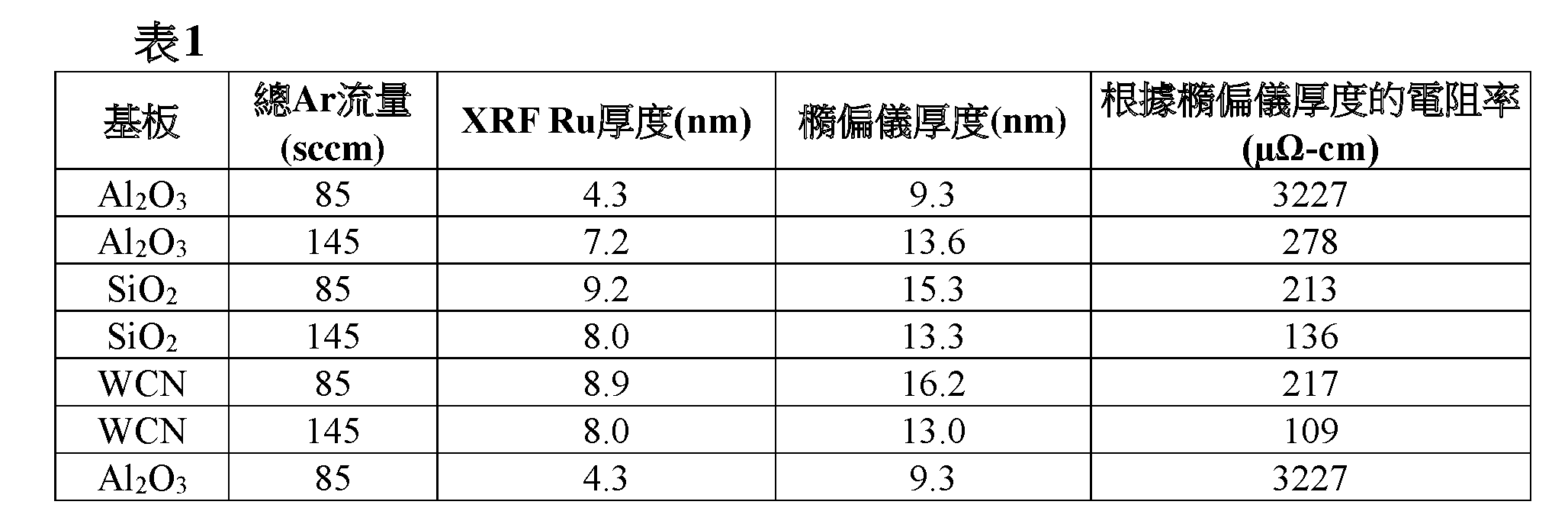
除了Al2O3,吹掃氣流動速率對生長速率(厚度)無顯著影響。而吹掃氣流動速率確實對所形成之Ru膜之電阻率有影響。咸信電阻率隨Ar氣體流動速率增加而降低,此係由於吹掃之增加可促進自膜表面移除配位體副產物。 Except for Al 2 O 3 , the purge gas flow rate has no significant effect on the growth rate (thickness). However, the purge gas flow rate does have an effect on the resistivity of the formed Ru film. It is believed that the resistivity decreases with increasing Ar gas flow rate because the increase in purge can promote the removal of ligand byproducts from the film surface.
SiO2、WCN及Al2O3三個基板上之含Ru膜係經由上文所述之脈衝式CVD方法以各種吹掃氣遞送時間不使用共反應物來製備。沈積循環順序如下:RuDMBD脈衝/吹掃時間:5秒/120秒至300秒。基板溫度為215℃且沈積壓力為1.4托。脈衝次數為95-110。形成於基板SiO2及WCN上之Ru膜之厚度在9nm至13nm範圍內。形成於基板Al2O3上之Ru膜之厚度在3.5nm至9.4nm範圍內。Ru膜厚度係藉由XRF測定。 Ru-containing films on three substrates of SiO 2 , WCN and Al 2 O 3 were prepared by the pulsed CVD method described above with various purge gas delivery times without the use of co-reactants. The deposition cycle sequence was as follows: RuDMBD pulse/purge time: 5 sec/120 sec to 300 sec. The substrate temperature was 215°C and the deposition pressure was 1.4 Torr. The number of pulses was 95-110. The thickness of the Ru film formed on the substrates SiO 2 and WCN was in the range of 9nm to 13nm. The thickness of the Ru film formed on the substrate Al 2 O 3 was in the range of 3.5nm to 9.4nm. The Ru film thickness was measured by XRF.
量測所形成之Ru膜之生長速率且結果示於圖4中。除了Al2O3,生長速率並未隨著測試範圍內的吹掃時間發生顯著變化,生長速 率隨吹掃時間增加而快速下降的情況可能歸因於RuDMBD在Al2O3表面上之解離較慢,且因此成核延遲更長,導致前驅體之解吸隨著吹掃時間的延長而增加。 The growth rate of the formed Ru films was measured and the results are shown in Figure 4. With the exception of Al2O3 , the growth rate did not vary significantly with the purge time within the tested range. The rapid decrease in growth rate with increasing purge time could be attributed to the slower dissociation of RuDMBD on the Al2O3 surface and thus longer nucleation delay, resulting in an increase in the desorption of the precursor with increasing purge time.
SiO2、WCN及Al2O3三個基板上之含Ru膜係經由上文所述之脈衝式CVD方法以各種吹掃氣遞送時間不使用共反應物來製備。沈積循環順序如下:RuDMBD脈衝/吹掃時間:5秒/120秒至300秒。基板溫度為215℃且沈積壓力為1.4托。脈衝次數為95-110。形成於基板SiO2及WCN上之Ru膜之厚度在9nm至13nm範圍內。形成於基板Al2O3上之Ru膜之厚度在3.5nm至9.4nm範圍內。Ru膜厚度係藉由XRF測定。 Ru-containing films on three substrates of SiO 2 , WCN and Al 2 O 3 were prepared by the pulsed CVD method described above with various purge gas delivery times without the use of co-reactants. The deposition cycle sequence was as follows: RuDMBD pulse/purge time: 5 sec/120 sec to 300 sec. The substrate temperature was 215°C and the deposition pressure was 1.4 Torr. The number of pulses was 95-110. The thickness of the Ru film formed on the substrates SiO 2 and WCN was in the range of 9nm to 13nm. The thickness of the Ru film formed on the substrate Al 2 O 3 was in the range of 3.5nm to 9.4nm. The Ru film thickness was measured by XRF.
量測沈積態Ru膜(「沈積態」膜)之電阻率。如上文所描述,使該等Ru膜經歷進一步退火,且量測經退火膜(「經400℃ Ar退火」膜)之電阻率。圖5A顯示吹掃時間對生長於Al2O3基板上之膜的電阻率的影響。圖5B顯示吹掃時間對生長於SiO2基板上之膜的電阻率的影響。圖5C顯示吹掃時間對生長於WCN基板上之膜的電阻率的影響。在全部三個不同基板上,沈積態膜之電阻率隨吹掃時間的增加而快速降低。經退火膜的電阻率同樣較低,例如約20μΩ-cm。 The resistivity of the deposited Ru films ("as deposited" films) was measured. The Ru films were subjected to further annealing as described above, and the resistivity of the annealed films ("400°C Ar annealed" films) was measured. FIG. 5A shows the effect of purge time on the resistivity of the film grown on an Al2O3 substrate. FIG. 5B shows the effect of purge time on the resistivity of the film grown on an SiO2 substrate. FIG. 5C shows the effect of purge time on the resistivity of the film grown on a WCN substrate. On all three different substrates, the resistivity of the deposited films decreases rapidly with increasing purge time. The resistivity of the annealed films is also low, for example, about 20 μΩ-cm.
SiO2、WCN及Al2O3三個基板上之含Ru膜係經由上文所述之脈衝式CVD方法以不同之脈衝時間不使用共反應物來製備。沈積循環順序如下:RuDMBD脈衝/吹掃時間:3秒至9秒/240秒。基板溫度為215℃。脈衝次數為100。 Ru-containing films on SiO 2 , WCN and Al 2 O 3 substrates were prepared by the pulsed CVD method described above with different pulse times without co-reactants. The deposition cycle sequence was as follows: RuDMBD pulse/purge time: 3 seconds to 9 seconds/240 seconds. Substrate temperature was 215°C. Number of pulses was 100.
量測沈積態Ru膜(「沈積態」膜)之生長速率。如上文所描 述,使形成於SiO2及WCN基板上之Ru膜經歷進一步退火,且量測經退火膜(「經400℃ Ar退火」膜)之生長速率。圖6A展示RuDMBD之脈衝時間對生長於全部三個基板上之膜的生長速率之影響。圖6B展示RuDMBD之脈衝時間對生長於SiO2基板上之沈積態及經退火膜之生長速率之影響。圖6C展示RuDMBD之脈衝時間對生長於WCN基板上之沈積態及經退火膜之生長速率之影響。觀測到低於前驅體之熱分解溫度之部分自限性生長狀態。生長速率不像ALD那樣完全飽和,但亦不像純CVD製程那樣呈線性。 The growth rate of the deposited Ru films ("as deposited" films) was measured. As described above, the Ru films formed on SiO2 and WCN substrates were further annealed, and the growth rate of the annealed films ("400°C Ar annealed" films) was measured. Figure 6A shows the effect of the pulse time of RuDMBD on the growth rate of the films grown on all three substrates. Figure 6B shows the effect of the pulse time of RuDMBD on the growth rate of the deposited and annealed films grown on SiO2 substrate. Figure 6C shows the effect of the pulse time of RuDMBD on the growth rate of the deposited and annealed films grown on WCN substrate. A partially self-limited growth state below the thermal decomposition temperature of the precursor was observed. The growth rate is not completely saturated like ALD, but it is not linear like a pure CVD process.
SiO2、WCN及Al2O3三個基板上之含Ru膜係經由上文所述之脈衝式CVD方法在不同之基板溫度下不使用共反應物來製備。沈積循環順序如下:RuDMBD脈衝/吹掃時間:5秒/240秒。沈積壓力為1.4托。各種基板溫度下之脈衝次數如下:185℃下,120次脈衝;200℃至230℃下,100次脈衝;250℃下,65次脈衝;及300℃下,30次脈衝。 Ru-containing films on three substrates, SiO 2 , WCN, and Al 2 O 3, were prepared by the pulsed CVD method described above without co-reactants at different substrate temperatures. The deposition cycle sequence was as follows: RuDMBD pulse/purge time: 5 sec/240 sec. The deposition pressure was 1.4 Torr. The number of pulses at various substrate temperatures was as follows: 120 pulses at 185°C; 100 pulses at 200°C to 230°C; 65 pulses at 250°C; and 30 pulses at 300°C.
量測沈積態Ru膜(「沈積態」膜)之生長速率。如上文所描述,使形成於SiO2基板上之Ru膜經歷進一步退火,且量測經退火膜(「經400℃ Ar退火」膜)之生長速率。圖7A展示基板溫度對生長於全部三個基板上之膜的生長速率(藉由XRF測定)的影響。圖7B展示基板溫度對生長於SiO2基板上之沈積態及退火膜之生長速率(如藉由橢偏儀法所測定)的影響。在SiO2及WCN基板上,低於約230℃之生長速率沒有較強的溫度依從性。所觀測到的約250℃或更高溫度下生長速率之快速增加係歸因於熱分解。 The growth rate of the deposited Ru films ("as deposited" films) was measured. As described above, the Ru films formed on the SiO2 substrate were subjected to further annealing, and the growth rate of the annealed films ("400°C Ar annealed" films) was measured. Figure 7A shows the effect of substrate temperature on the growth rate (measured by XRF) of the films grown on all three substrates. Figure 7B shows the effect of substrate temperature on the growth rate (as measured by ellipsometry) of the deposited and annealed films grown on the SiO2 substrate. On the SiO2 and WCN substrates, there is no strong temperature dependence of the growth rate below about 230°C. The observed rapid increase in growth rate at temperatures of about 250°C or higher is attributed to thermal decomposition.
SiO2、WCN及Al2O3三個基板上之含Ru膜係經由上文實例8中所描述之脈衝式CVD方法來製備。 The Ru-containing films on the three substrates of SiO 2 , WCN and Al 2 O 3 were prepared by the pulsed CVD method described in Example 8 above.
量測沈積態Ru膜(「沈積態」膜)之電阻率。如上文所描述,使該等Ru膜經歷進一步退火,且量測經退火膜(「經400℃ Ar退火」膜)之電阻率。圖8A顯示基板溫度對生長於Al2O3基板上之膜之電阻率的影響。圖8B顯示基板溫度對生長於SiO2基板上之膜之電阻率的影響。圖8C顯示基板溫度對生長於WCN基板上之膜之電阻率的影響。在215℃-230℃下觀測到最佳沈積溫度,其接近或低於RuDMBD前驅體之熱分解溫度。經退火之膜展現最低電阻率。在高於230℃之沈積溫度下,一些膜在退火之後變得不均勻且出現高電阻率區域。 The resistivity of the as-deposited Ru films ("as-deposited" films) was measured. The Ru films were subjected to further annealing as described above, and the resistivity of the annealed films ("400°C Ar annealed" films) was measured. FIG. 8A shows the effect of substrate temperature on the resistivity of films grown on Al2O3 substrates . FIG. 8B shows the effect of substrate temperature on the resistivity of films grown on SiO2 substrates. FIG. 8C shows the effect of substrate temperature on the resistivity of films grown on WCN substrates. The optimum deposition temperature was observed at 215°C-230°C, which is close to or below the thermal decomposition temperature of the RuDMBD precursor. The annealed films exhibited the lowest resistivity. At deposition temperatures above 230°C, some films became non-uniform after annealing and exhibited high-resistivity regions.
SiO2、WCN及Al2O3三個基板上之含Ru膜係經由上文所述之脈衝式CVD方法使用NH3作為共反應物及不使用共反應物來製備。無NH3共反應物之沈積循環順序如下:RuDMBD脈衝/吹掃時間:5秒/240秒。伴隨NH3共反應物之沈積循環順序如下:RuDMBD脈衝/吹掃時間/NH3脈衝/吹掃時間:5秒/120秒/5秒/115秒。基板溫度為230℃且沈積壓力為1.4托。沈積循環數在25個循環至100個循環之間變化。 Ru-containing films on three substrates of SiO 2 , WCN and Al 2 O 3 were prepared by the pulsed CVD method described above with and without NH 3 as co-reactant. The deposition cycle sequence without NH 3 co-reactant was as follows: RuDMBD pulse/purge time: 5 sec/240 sec. The deposition cycle sequence with NH 3 co-reactant was as follows: RuDMBD pulse/purge time/NH 3 pulse/purge time: 5 sec/120 sec/5 sec/115 sec. The substrate temperature was 230°C and the deposition pressure was 1.4 Torr. The number of deposition cycles varied from 25 cycles to 100 cycles.
量測所形成之Ru膜之Ru膜厚度(如藉由XRF所測定)。圖9A顯示循環次數對生長於Al2O3基板上之膜之Ru膜厚度的影響。圖9B顯示循環數對生長於基板SiO2上之膜之Ru膜厚度的影響。圖9C顯示循環數對生長於WCN基板上之膜之Ru膜厚度的影響。NH3在較短吹掃時間(諸如對於RuDMBD,10秒)內,對生長速率具有極小影響,但在較長吹掃時間 內,諸如60-120秒,由於其與Ru之反應性,可顯著增加生長速率;因此,在所有3種不同基板上引起成核延遲較短且線性斜率略微增加。 The Ru film thickness of the formed Ru films was measured (as determined by XRF). FIG. 9A shows the effect of the number of cycles on the Ru film thickness of the film grown on an Al 2 O 3 substrate. FIG. 9B shows the effect of the number of cycles on the Ru film thickness of the film grown on a SiO 2 substrate. FIG. 9C shows the effect of the number of cycles on the Ru film thickness of the film grown on a WCN substrate. NH 3 has little effect on the growth rate at short purge times (e.g., 10 seconds for RuDMBD), but significantly increases the growth rate at longer purge times, such as 60-120 seconds, due to its reactivity with Ru; thus, causing shorter nucleation delays and slightly increased linear slopes on all 3 different substrates.
SiO2及WCN兩個基板上之含Ru膜係經由上文所述之脈衝式CVD方法使用NH3作為共反應物及不使用共反應物來製備。無NH3共反應物之沈積循環順序如下:RuDMBD脈衝/吹掃時間:5秒/120秒。伴隨NH3共反應物之沈積循環順序如下:RuDMBD脈衝/吹掃時間/NH3脈衝/吹掃時間:5秒/60秒/5秒/55秒。基板溫度為230℃且沈積壓力為1.4托。 Ru-containing films on both SiO2 and WCN substrates were prepared by the pulsed CVD method described above with and without NH3 as co-reactant. The deposition cycle sequence without NH3 co-reactant was as follows: RuDMBD pulse/purge time: 5 sec/120 sec. The deposition cycle sequence with NH3 co-reactant was as follows: RuDMBD pulse/purge time/ NH3 pulse/purge time: 5 sec/60 sec/5 sec/55 sec. The substrate temperature was 230°C and the deposition pressure was 1.4 Torr.
量測沈積態Ru膜(「沈積態Ru」膜)之電阻率。如上文所描述,使該等Ru膜經歷進一步退火,且量測經退火膜(「經400℃ Ar退火」膜)之電阻率。圖10A顯示Ru膜厚度(如藉由XRF所量測)對SiO2及WCN上之沈積態膜之電阻率的影響。圖10B展示Ru膜厚度(如藉由XRF所量測)對SiO2及WCN上之經400℃ Ar退火膜之電阻率的影響。NH3在諸如10秒之短吹掃時間內可不與RuDMBD反應且X射線光電子光譜法(XPS)未發現N。在60秒之更長之吹掃時間內,在使用NH3共反應物形成之SiO2上的沈積態膜中發現約6原子% N。相比於10nm之相同厚度之無共反應物之Ru膜,N併入導致電阻率增加。在經400℃ Ar退火之後,N被完全移除且無法被XPS檢測到,且因此膜電阻率達至與經退火之無共反應物Ru之電阻率相同的水準。 The resistivity of the as-deposited Ru films ("as-deposited Ru" films) was measured. As described above, the Ru films were subjected to further annealing, and the resistivity of the annealed films ("400°C Ar annealed" films) was measured. FIG. 10A shows the effect of Ru film thickness (as measured by XRF) on the resistivity of the as-deposited films on SiO2 and WCN. FIG. 10B shows the effect of Ru film thickness (as measured by XRF) on the resistivity of the 400°C Ar annealed films on SiO2 and WCN. NH3 may not react with RuDMBD within a short purge time such as 10 seconds and no N was found by X-ray photoelectron spectroscopy (XPS). At longer purge times of 60 seconds, about 6 atomic % N was found in the as-deposited film on SiO2 formed using NH3 co-reactant. N incorporation resulted in an increase in resistivity compared to the same thickness of 10 nm Ru film without co-reactant. After 400°C Ar annealing, N was completely removed and could not be detected by XPS, and thus the film resistivity reached the same level as that of the annealed Ru without co-reactant.
本說明書中所提及之所有公開案、專利申請案、頒予專利及其他文獻均以引用之方式併入本文中,該引用程度就如同已特定地且個別地將各個別公開案、專利申請案、頒予專利或其他文獻以全文引用之方式併入一般。以引用之方式併入之文本中所含之定義若與本發明中之定義 矛盾,則將其排除在外。 All publications, patent applications, issued patents, and other documents mentioned in this specification are incorporated herein by reference to the same extent as if each individual publication, patent application, issued patent, or other document had been specifically and individually incorporated by reference in its entirety. Definitions contained in texts incorporated by reference will be excluded if they conflict with definitions in this invention.
措辭「包含(comprise/comprises/comprising)」應解釋為包括在內而非排他性的。 The words "comprise/comprises/comprising" should be construed as inclusive rather than exclusive.
Claims (21)
Applications Claiming Priority (2)
| Application Number | Priority Date | Filing Date | Title |
|---|---|---|---|
| US202063046911P | 2020-07-01 | 2020-07-01 | |
| US63/046,911 | 2020-07-01 |
Publications (2)
| Publication Number | Publication Date |
|---|---|
| TW202212607A TW202212607A (en) | 2022-04-01 |
| TWI877383B true TWI877383B (en) | 2025-03-21 |
Family
ID=76845194
Family Applications (1)
| Application Number | Title | Priority Date | Filing Date |
|---|---|---|---|
| TW110123500A TWI877383B (en) | 2020-07-01 | 2021-06-28 | Methods of forming ruthenium-containing films without a co-reactant |
Country Status (6)
| Country | Link |
|---|---|
| US (1) | US20230227966A1 (en) |
| JP (1) | JP7761602B2 (en) |
| KR (1) | KR20230033713A (en) |
| CN (1) | CN115735019A (en) |
| TW (1) | TWI877383B (en) |
| WO (1) | WO2022002809A1 (en) |
Families Citing this family (1)
| Publication number | Priority date | Publication date | Assignee | Title |
|---|---|---|---|---|
| CN120649006B (en) * | 2025-08-21 | 2025-11-21 | 合肥安德科铭半导体科技有限公司 | A method for atomic layer deposition of Ru-containing thin films |
Citations (1)
| Publication number | Priority date | Publication date | Assignee | Title |
|---|---|---|---|---|
| US20130202794A1 (en) * | 2010-07-22 | 2013-08-08 | American Air Liquide, Inc. | Metal film deposition |
Family Cites Families (5)
| Publication number | Priority date | Publication date | Assignee | Title |
|---|---|---|---|---|
| JP4661130B2 (en) * | 2004-08-17 | 2011-03-30 | Jsr株式会社 | Chemical vapor deposition method |
| TW200951241A (en) * | 2008-05-30 | 2009-12-16 | Sigma Aldrich Co | Methods of forming ruthenium-containing films by atomic layer deposition |
| US9249505B2 (en) * | 2013-06-28 | 2016-02-02 | Wayne State University | Bis(trimethylsilyl) six-membered ring systems and related compounds as reducing agents for forming layers on a substrate |
| JP7346430B2 (en) | 2018-02-12 | 2023-09-19 | メルク パテント ゲゼルシャフト ミット ベシュレンクテル ハフツング | Ruthenium deposition method using oxygen-free co-reactants |
| CN113039309A (en) * | 2018-11-15 | 2021-06-25 | 恩特格里斯公司 | Plasma Enhanced Atomic Layer Deposition (PEALD) process using ruthenium precursors |
-
2021
- 2021-06-28 WO PCT/EP2021/067605 patent/WO2022002809A1/en not_active Ceased
- 2021-06-28 TW TW110123500A patent/TWI877383B/en active
- 2021-06-28 JP JP2022581519A patent/JP7761602B2/en active Active
- 2021-06-28 US US18/011,737 patent/US20230227966A1/en not_active Abandoned
- 2021-06-28 KR KR1020237003578A patent/KR20230033713A/en active Pending
- 2021-06-28 CN CN202180045051.4A patent/CN115735019A/en active Pending
Patent Citations (1)
| Publication number | Priority date | Publication date | Assignee | Title |
|---|---|---|---|---|
| US20130202794A1 (en) * | 2010-07-22 | 2013-08-08 | American Air Liquide, Inc. | Metal film deposition |
Also Published As
| Publication number | Publication date |
|---|---|
| JP2023532534A (en) | 2023-07-28 |
| CN115735019A (en) | 2023-03-03 |
| WO2022002809A1 (en) | 2022-01-06 |
| JP7761602B2 (en) | 2025-10-28 |
| KR20230033713A (en) | 2023-03-08 |
| TW202212607A (en) | 2022-04-01 |
| US20230227966A1 (en) | 2023-07-20 |
Similar Documents
| Publication | Publication Date | Title |
|---|---|---|
| TWI869337B (en) | Methods of vapor deposition of ruthenium using an oxygen-free co-reactant | |
| CN111032908B (en) | Atomic layer deposition method for selective film growth | |
| JP7716432B2 (en) | Method for forming a molybdenum-containing film deposited on a metal element film | |
| CN101801987B (en) | Methods of forming thin metal-containing films by CVD | |
| CN102084026A (en) | Methods of forming ruthenium-containing films by atomic layer deposition | |
| TWI693229B (en) | Zirconium-containing film forming compositions for vapor deposition of zirconium-containing films | |
| TWI872188B (en) | Ruthenium-containing films deposited on ruthenium-titanium nitride films and methods of forming the same | |
| TWI877383B (en) | Methods of forming ruthenium-containing films without a co-reactant | |
| US11293093B2 (en) | Water assisted highly pure ruthenium thin film deposition | |
| KR102815650B1 (en) | Precursor containing group iv transition metal and deposition method of film using the same | |
| JP2023502418A (en) | Compounds and methods for selectively forming metal-containing films |