KR20240077524A - Display device - Google Patents
Display device Download PDFInfo
- Publication number
- KR20240077524A KR20240077524A KR1020220157430A KR20220157430A KR20240077524A KR 20240077524 A KR20240077524 A KR 20240077524A KR 1020220157430 A KR1020220157430 A KR 1020220157430A KR 20220157430 A KR20220157430 A KR 20220157430A KR 20240077524 A KR20240077524 A KR 20240077524A
- Authority
- KR
- South Korea
- Prior art keywords
- fan
- out line
- lines
- line
- display device
- Prior art date
- Legal status (The legal status is an assumption and is not a legal conclusion. Google has not performed a legal analysis and makes no representation as to the accuracy of the status listed.)
- Pending
Links
Images


Classifications
-
- G—PHYSICS
- G09—EDUCATION; CRYPTOGRAPHY; DISPLAY; ADVERTISING; SEALS
- G09G—ARRANGEMENTS OR CIRCUITS FOR CONTROL OF INDICATING DEVICES USING STATIC MEANS TO PRESENT VARIABLE INFORMATION
- G09G3/00—Control arrangements or circuits, of interest only in connection with visual indicators other than cathode-ray tubes
- G09G3/20—Control arrangements or circuits, of interest only in connection with visual indicators other than cathode-ray tubes for presentation of an assembly of a number of characters, e.g. a page, by composing the assembly by combination of individual elements arranged in a matrix no fixed position being assigned to or needed to be assigned to the individual characters or partial characters
- G09G3/22—Control arrangements or circuits, of interest only in connection with visual indicators other than cathode-ray tubes for presentation of an assembly of a number of characters, e.g. a page, by composing the assembly by combination of individual elements arranged in a matrix no fixed position being assigned to or needed to be assigned to the individual characters or partial characters using controlled light sources
- G09G3/30—Control arrangements or circuits, of interest only in connection with visual indicators other than cathode-ray tubes for presentation of an assembly of a number of characters, e.g. a page, by composing the assembly by combination of individual elements arranged in a matrix no fixed position being assigned to or needed to be assigned to the individual characters or partial characters using controlled light sources using electroluminescent panels
- G09G3/32—Control arrangements or circuits, of interest only in connection with visual indicators other than cathode-ray tubes for presentation of an assembly of a number of characters, e.g. a page, by composing the assembly by combination of individual elements arranged in a matrix no fixed position being assigned to or needed to be assigned to the individual characters or partial characters using controlled light sources using electroluminescent panels semiconductive, e.g. using light-emitting diodes [LED]
- G09G3/3208—Control arrangements or circuits, of interest only in connection with visual indicators other than cathode-ray tubes for presentation of an assembly of a number of characters, e.g. a page, by composing the assembly by combination of individual elements arranged in a matrix no fixed position being assigned to or needed to be assigned to the individual characters or partial characters using controlled light sources using electroluminescent panels semiconductive, e.g. using light-emitting diodes [LED] organic, e.g. using organic light-emitting diodes [OLED]
- G09G3/3225—Control arrangements or circuits, of interest only in connection with visual indicators other than cathode-ray tubes for presentation of an assembly of a number of characters, e.g. a page, by composing the assembly by combination of individual elements arranged in a matrix no fixed position being assigned to or needed to be assigned to the individual characters or partial characters using controlled light sources using electroluminescent panels semiconductive, e.g. using light-emitting diodes [LED] organic, e.g. using organic light-emitting diodes [OLED] using an active matrix
- G09G3/3233—Control arrangements or circuits, of interest only in connection with visual indicators other than cathode-ray tubes for presentation of an assembly of a number of characters, e.g. a page, by composing the assembly by combination of individual elements arranged in a matrix no fixed position being assigned to or needed to be assigned to the individual characters or partial characters using controlled light sources using electroluminescent panels semiconductive, e.g. using light-emitting diodes [LED] organic, e.g. using organic light-emitting diodes [OLED] using an active matrix with pixel circuitry controlling the current through the light-emitting element
-
- H—ELECTRICITY
- H10—SEMICONDUCTOR DEVICES; ELECTRIC SOLID-STATE DEVICES NOT OTHERWISE PROVIDED FOR
- H10K—ORGANIC ELECTRIC SOLID-STATE DEVICES
- H10K59/00—Integrated devices, or assemblies of multiple devices, comprising at least one organic light-emitting element covered by group H10K50/00
- H10K59/10—OLED displays
- H10K59/12—Active-matrix OLED [AMOLED] displays
- H10K59/131—Interconnections, e.g. wiring lines or terminals
-
- G—PHYSICS
- G09—EDUCATION; CRYPTOGRAPHY; DISPLAY; ADVERTISING; SEALS
- G09G—ARRANGEMENTS OR CIRCUITS FOR CONTROL OF INDICATING DEVICES USING STATIC MEANS TO PRESENT VARIABLE INFORMATION
- G09G3/00—Control arrangements or circuits, of interest only in connection with visual indicators other than cathode-ray tubes
- G09G3/006—Electronic inspection or testing of displays and display drivers, e.g. of LED or LCD displays
-
- G—PHYSICS
- G09—EDUCATION; CRYPTOGRAPHY; DISPLAY; ADVERTISING; SEALS
- G09G—ARRANGEMENTS OR CIRCUITS FOR CONTROL OF INDICATING DEVICES USING STATIC MEANS TO PRESENT VARIABLE INFORMATION
- G09G3/00—Control arrangements or circuits, of interest only in connection with visual indicators other than cathode-ray tubes
- G09G3/03—Control arrangements or circuits, of interest only in connection with visual indicators other than cathode-ray tubes specially adapted for displays having non-planar surfaces, e.g. curved displays
- G09G3/035—Control arrangements or circuits, of interest only in connection with visual indicators other than cathode-ray tubes specially adapted for displays having non-planar surfaces, e.g. curved displays for flexible display surfaces
-
- G—PHYSICS
- G09—EDUCATION; CRYPTOGRAPHY; DISPLAY; ADVERTISING; SEALS
- G09G—ARRANGEMENTS OR CIRCUITS FOR CONTROL OF INDICATING DEVICES USING STATIC MEANS TO PRESENT VARIABLE INFORMATION
- G09G3/00—Control arrangements or circuits, of interest only in connection with visual indicators other than cathode-ray tubes
- G09G3/20—Control arrangements or circuits, of interest only in connection with visual indicators other than cathode-ray tubes for presentation of an assembly of a number of characters, e.g. a page, by composing the assembly by combination of individual elements arranged in a matrix no fixed position being assigned to or needed to be assigned to the individual characters or partial characters
- G09G3/2092—Details of a display terminals using a flat panel, the details relating to the control arrangement of the display terminal and to the interfaces thereto
-
- G—PHYSICS
- G09—EDUCATION; CRYPTOGRAPHY; DISPLAY; ADVERTISING; SEALS
- G09G—ARRANGEMENTS OR CIRCUITS FOR CONTROL OF INDICATING DEVICES USING STATIC MEANS TO PRESENT VARIABLE INFORMATION
- G09G3/00—Control arrangements or circuits, of interest only in connection with visual indicators other than cathode-ray tubes
- G09G3/20—Control arrangements or circuits, of interest only in connection with visual indicators other than cathode-ray tubes for presentation of an assembly of a number of characters, e.g. a page, by composing the assembly by combination of individual elements arranged in a matrix no fixed position being assigned to or needed to be assigned to the individual characters or partial characters
- G09G3/22—Control arrangements or circuits, of interest only in connection with visual indicators other than cathode-ray tubes for presentation of an assembly of a number of characters, e.g. a page, by composing the assembly by combination of individual elements arranged in a matrix no fixed position being assigned to or needed to be assigned to the individual characters or partial characters using controlled light sources
- G09G3/30—Control arrangements or circuits, of interest only in connection with visual indicators other than cathode-ray tubes for presentation of an assembly of a number of characters, e.g. a page, by composing the assembly by combination of individual elements arranged in a matrix no fixed position being assigned to or needed to be assigned to the individual characters or partial characters using controlled light sources using electroluminescent panels
- G09G3/32—Control arrangements or circuits, of interest only in connection with visual indicators other than cathode-ray tubes for presentation of an assembly of a number of characters, e.g. a page, by composing the assembly by combination of individual elements arranged in a matrix no fixed position being assigned to or needed to be assigned to the individual characters or partial characters using controlled light sources using electroluminescent panels semiconductive, e.g. using light-emitting diodes [LED]
-
- H—ELECTRICITY
- H10—SEMICONDUCTOR DEVICES; ELECTRIC SOLID-STATE DEVICES NOT OTHERWISE PROVIDED FOR
- H10D—INORGANIC ELECTRIC SEMICONDUCTOR DEVICES
- H10D86/00—Integrated devices formed in or on insulating or conducting substrates, e.g. formed in silicon-on-insulator [SOI] substrates or on stainless steel or glass substrates
- H10D86/40—Integrated devices formed in or on insulating or conducting substrates, e.g. formed in silicon-on-insulator [SOI] substrates or on stainless steel or glass substrates characterised by multiple TFTs
- H10D86/441—Interconnections, e.g. scanning lines
-
- H—ELECTRICITY
- H10—SEMICONDUCTOR DEVICES; ELECTRIC SOLID-STATE DEVICES NOT OTHERWISE PROVIDED FOR
- H10D—INORGANIC ELECTRIC SEMICONDUCTOR DEVICES
- H10D86/00—Integrated devices formed in or on insulating or conducting substrates, e.g. formed in silicon-on-insulator [SOI] substrates or on stainless steel or glass substrates
- H10D86/40—Integrated devices formed in or on insulating or conducting substrates, e.g. formed in silicon-on-insulator [SOI] substrates or on stainless steel or glass substrates characterised by multiple TFTs
- H10D86/60—Integrated devices formed in or on insulating or conducting substrates, e.g. formed in silicon-on-insulator [SOI] substrates or on stainless steel or glass substrates characterised by multiple TFTs wherein the TFTs are in active matrices
-
- H—ELECTRICITY
- H10—SEMICONDUCTOR DEVICES; ELECTRIC SOLID-STATE DEVICES NOT OTHERWISE PROVIDED FOR
- H10H—INORGANIC LIGHT-EMITTING SEMICONDUCTOR DEVICES HAVING POTENTIAL BARRIERS
- H10H29/00—Integrated devices, or assemblies of multiple devices, comprising at least one light-emitting semiconductor element covered by group H10H20/00
- H10H29/10—Integrated devices comprising at least one light-emitting semiconductor component covered by group H10H20/00
- H10H29/14—Integrated devices comprising at least one light-emitting semiconductor component covered by group H10H20/00 comprising multiple light-emitting semiconductor components
- H10H29/142—Two-dimensional arrangements, e.g. asymmetric LED layout
-
- H—ELECTRICITY
- H10—SEMICONDUCTOR DEVICES; ELECTRIC SOLID-STATE DEVICES NOT OTHERWISE PROVIDED FOR
- H10K—ORGANIC ELECTRIC SOLID-STATE DEVICES
- H10K59/00—Integrated devices, or assemblies of multiple devices, comprising at least one organic light-emitting element covered by group H10K50/00
- H10K59/10—OLED displays
- H10K59/12—Active-matrix OLED [AMOLED] displays
- H10K59/121—Active-matrix OLED [AMOLED] displays characterised by the geometry or disposition of pixel elements
-
- H—ELECTRICITY
- H10—SEMICONDUCTOR DEVICES; ELECTRIC SOLID-STATE DEVICES NOT OTHERWISE PROVIDED FOR
- H10K—ORGANIC ELECTRIC SOLID-STATE DEVICES
- H10K59/00—Integrated devices, or assemblies of multiple devices, comprising at least one organic light-emitting element covered by group H10K50/00
- H10K59/10—OLED displays
- H10K59/12—Active-matrix OLED [AMOLED] displays
- H10K59/129—Chiplets
-
- H—ELECTRICITY
- H10—SEMICONDUCTOR DEVICES; ELECTRIC SOLID-STATE DEVICES NOT OTHERWISE PROVIDED FOR
- H10K—ORGANIC ELECTRIC SOLID-STATE DEVICES
- H10K77/00—Constructional details of devices covered by this subclass and not covered by groups H10K10/80, H10K30/80, H10K50/80 or H10K59/80
- H10K77/10—Substrates, e.g. flexible substrates
- H10K77/111—Flexible substrates
-
- G—PHYSICS
- G09—EDUCATION; CRYPTOGRAPHY; DISPLAY; ADVERTISING; SEALS
- G09G—ARRANGEMENTS OR CIRCUITS FOR CONTROL OF INDICATING DEVICES USING STATIC MEANS TO PRESENT VARIABLE INFORMATION
- G09G2300/00—Aspects of the constitution of display devices
- G09G2300/04—Structural and physical details of display devices
- G09G2300/0421—Structural details of the set of electrodes
- G09G2300/0426—Layout of electrodes and connections
-
- G—PHYSICS
- G09—EDUCATION; CRYPTOGRAPHY; DISPLAY; ADVERTISING; SEALS
- G09G—ARRANGEMENTS OR CIRCUITS FOR CONTROL OF INDICATING DEVICES USING STATIC MEANS TO PRESENT VARIABLE INFORMATION
- G09G2300/00—Aspects of the constitution of display devices
- G09G2300/08—Active matrix structure, i.e. with use of active elements, inclusive of non-linear two terminal elements, in the pixels together with light emitting or modulating elements
- G09G2300/0809—Several active elements per pixel in active matrix panels
- G09G2300/0814—Several active elements per pixel in active matrix panels used for selection purposes, e.g. logical AND for partial update
-
- G—PHYSICS
- G09—EDUCATION; CRYPTOGRAPHY; DISPLAY; ADVERTISING; SEALS
- G09G—ARRANGEMENTS OR CIRCUITS FOR CONTROL OF INDICATING DEVICES USING STATIC MEANS TO PRESENT VARIABLE INFORMATION
- G09G2300/00—Aspects of the constitution of display devices
- G09G2300/08—Active matrix structure, i.e. with use of active elements, inclusive of non-linear two terminal elements, in the pixels together with light emitting or modulating elements
- G09G2300/0809—Several active elements per pixel in active matrix panels
- G09G2300/0819—Several active elements per pixel in active matrix panels used for counteracting undesired variations, e.g. feedback or autozeroing
-
- G—PHYSICS
- G09—EDUCATION; CRYPTOGRAPHY; DISPLAY; ADVERTISING; SEALS
- G09G—ARRANGEMENTS OR CIRCUITS FOR CONTROL OF INDICATING DEVICES USING STATIC MEANS TO PRESENT VARIABLE INFORMATION
- G09G2300/00—Aspects of the constitution of display devices
- G09G2300/08—Active matrix structure, i.e. with use of active elements, inclusive of non-linear two terminal elements, in the pixels together with light emitting or modulating elements
- G09G2300/0809—Several active elements per pixel in active matrix panels
- G09G2300/0842—Several active elements per pixel in active matrix panels forming a memory circuit, e.g. a dynamic memory with one capacitor
- G09G2300/0861—Several active elements per pixel in active matrix panels forming a memory circuit, e.g. a dynamic memory with one capacitor with additional control of the display period without amending the charge stored in a pixel memory, e.g. by means of additional select electrodes
- G09G2300/0866—Several active elements per pixel in active matrix panels forming a memory circuit, e.g. a dynamic memory with one capacitor with additional control of the display period without amending the charge stored in a pixel memory, e.g. by means of additional select electrodes by means of changes in the pixel supply voltage
-
- G—PHYSICS
- G09—EDUCATION; CRYPTOGRAPHY; DISPLAY; ADVERTISING; SEALS
- G09G—ARRANGEMENTS OR CIRCUITS FOR CONTROL OF INDICATING DEVICES USING STATIC MEANS TO PRESENT VARIABLE INFORMATION
- G09G2310/00—Command of the display device
- G09G2310/02—Addressing, scanning or driving the display screen or processing steps related thereto
- G09G2310/0264—Details of driving circuits
- G09G2310/0297—Special arrangements with multiplexing or demultiplexing of display data in the drivers for data electrodes, in a pre-processing circuitry delivering display data to said drivers or in the matrix panel, e.g. multiplexing plural data signals to one D/A converter or demultiplexing the D/A converter output to multiple columns
-
- G—PHYSICS
- G09—EDUCATION; CRYPTOGRAPHY; DISPLAY; ADVERTISING; SEALS
- G09G—ARRANGEMENTS OR CIRCUITS FOR CONTROL OF INDICATING DEVICES USING STATIC MEANS TO PRESENT VARIABLE INFORMATION
- G09G2320/00—Control of display operating conditions
- G09G2320/04—Maintaining the quality of display appearance
- G09G2320/043—Preventing or counteracting the effects of ageing
- G09G2320/045—Compensation of drifts in the characteristics of light emitting or modulating elements
-
- G—PHYSICS
- G09—EDUCATION; CRYPTOGRAPHY; DISPLAY; ADVERTISING; SEALS
- G09G—ARRANGEMENTS OR CIRCUITS FOR CONTROL OF INDICATING DEVICES USING STATIC MEANS TO PRESENT VARIABLE INFORMATION
- G09G3/00—Control arrangements or circuits, of interest only in connection with visual indicators other than cathode-ray tubes
- G09G3/20—Control arrangements or circuits, of interest only in connection with visual indicators other than cathode-ray tubes for presentation of an assembly of a number of characters, e.g. a page, by composing the assembly by combination of individual elements arranged in a matrix no fixed position being assigned to or needed to be assigned to the individual characters or partial characters
- G09G3/22—Control arrangements or circuits, of interest only in connection with visual indicators other than cathode-ray tubes for presentation of an assembly of a number of characters, e.g. a page, by composing the assembly by combination of individual elements arranged in a matrix no fixed position being assigned to or needed to be assigned to the individual characters or partial characters using controlled light sources
- G09G3/30—Control arrangements or circuits, of interest only in connection with visual indicators other than cathode-ray tubes for presentation of an assembly of a number of characters, e.g. a page, by composing the assembly by combination of individual elements arranged in a matrix no fixed position being assigned to or needed to be assigned to the individual characters or partial characters using controlled light sources using electroluminescent panels
- G09G3/32—Control arrangements or circuits, of interest only in connection with visual indicators other than cathode-ray tubes for presentation of an assembly of a number of characters, e.g. a page, by composing the assembly by combination of individual elements arranged in a matrix no fixed position being assigned to or needed to be assigned to the individual characters or partial characters using controlled light sources using electroluminescent panels semiconductive, e.g. using light-emitting diodes [LED]
- G09G3/3208—Control arrangements or circuits, of interest only in connection with visual indicators other than cathode-ray tubes for presentation of an assembly of a number of characters, e.g. a page, by composing the assembly by combination of individual elements arranged in a matrix no fixed position being assigned to or needed to be assigned to the individual characters or partial characters using controlled light sources using electroluminescent panels semiconductive, e.g. using light-emitting diodes [LED] organic, e.g. using organic light-emitting diodes [OLED]
- G09G3/3275—Details of drivers for data electrodes
-
- H—ELECTRICITY
- H10—SEMICONDUCTOR DEVICES; ELECTRIC SOLID-STATE DEVICES NOT OTHERWISE PROVIDED FOR
- H10K—ORGANIC ELECTRIC SOLID-STATE DEVICES
- H10K2102/00—Constructional details relating to the organic devices covered by this subclass
- H10K2102/301—Details of OLEDs
- H10K2102/311—Flexible OLED
Landscapes
- Engineering & Computer Science (AREA)
- Physics & Mathematics (AREA)
- Computer Hardware Design (AREA)
- General Physics & Mathematics (AREA)
- Theoretical Computer Science (AREA)
- Microelectronics & Electronic Packaging (AREA)
- Geometry (AREA)
- Devices For Indicating Variable Information By Combining Individual Elements (AREA)
Abstract
본 발명에 따른 표시장치는 표시패널 및 상기 표시패널 상에 실장된 구동칩을 포함한다. 표시패널은 베이스층, 화소들, 신호 라인들, 팬아웃 라인들, 및 선택 회로를 포함한다. 베이스층은 제1 영역, 밴딩축을 기준으로 밴딩되는 제2 영역 및 상기 제2 영역에 인접한 제3 영역을 포함한다. 화소들은 상기 제1 영역에 배치되고, 신호 라인들은 상기 제1 영역에 배치되고, 화소들에 연결된다. 팬아웃 라인들은 상기 제2 영역에 배치되고, 신호라인들에 연결된다. 선택 회로는 제3 영역에서 팬아웃 라인들과 상기 구동칩 사이에 배치되고, 팬아웃 라인들과 상기 구동칩에 연결된다.A display device according to the present invention includes a display panel and a driving chip mounted on the display panel. The display panel includes a base layer, pixels, signal lines, fan-out lines, and a selection circuit. The base layer includes a first region, a second region bent about the bending axis, and a third region adjacent to the second region. Pixels are placed in the first area, and signal lines are placed in the first area and connected to the pixels. Fan-out lines are arranged in the second area and connected to signal lines. A selection circuit is disposed between the fan-out lines and the driving chip in the third area, and is connected to the fan-out lines and the driving chip.
Description
본 발명은 표시 장치에 관한 것으로, 상세하게는 화질을 개선할 수 있는 표시 장치에 관한 것이다. The present invention relates to a display device, and more specifically to a display device capable of improving image quality.
텔레비전, 휴대 전화, 태블릿, 컴퓨터, 내비게이션, 게임기 등과 같은 멀티미디어 전자장치들은 영상을 표시하기 위한 표시패널을 구비한다. Multimedia electronic devices such as televisions, mobile phones, tablets, computers, navigation systems, game consoles, etc. are equipped with display panels for displaying images.
최근 시장에 요구에 따라 표시패널에서 영상을 표시하지 않는 영역을 축소하려는 연구가 진행되고 있다. 동시에 표시패널에서 사용자에게 영상이 표시되는 표시영역을 확대시키고 베젤을 감소시키기 위한 연구가 진행되고 있다.Recently, in response to market demands, research is being conducted to reduce the area where images are not displayed on the display panel. At the same time, research is underway to expand the display area where images are displayed to users on the display panel and reduce the bezel.
본 발명의 목적은 베젤을 감소시키면서 커플링에 의한 화질 저하를 방지할 수 있는 표시 장치를 제공하는 것이다.The purpose of the present invention is to provide a display device that can prevent image quality degradation due to coupling while reducing the bezel.
본 발명의 일 특징에 따른 표시 장치는 표시패널 및 상기 표시패널 상에 실장된 구동칩을 포함한다. 상기 표시패널은, 베이스층, 화소들, 신호 라인들, 복수의 팬아웃 라인들, 및 선택 회로를 포함한다.A display device according to one aspect of the present invention includes a display panel and a driving chip mounted on the display panel. The display panel includes a base layer, pixels, signal lines, a plurality of fan-out lines, and a selection circuit.
베이스층은 제1 영역, 상기 제1 영역에 인접하고 밴딩축을 기준으로 밴딩되는 제2 영역 및 상기 제2 영역에 인접한 제3 영역을 포함한다. 복수의 화소들은 상기 제1 영역에 배치되고, 복수의 신호 라인들은 상기 제1 영역에 배치되고, 상기 복수의 화소들에 연결된다. 복수의 팬아웃 라인들은 상기 제2 영역에 배치되고, 상기 복수의 신호라인들에 연결된다. 선택 회로는 제3 영역에서 상기 복수의 팬아웃 라인들과 상기 구동칩 사이에 배치되고, 상기 복수의 팬아웃 라인들과 상기 구동칩에 연결된다. The base layer includes a first region, a second region adjacent to the first region and bent about a bending axis, and a third region adjacent to the second region. A plurality of pixels are arranged in the first area, and a plurality of signal lines are arranged in the first area and connected to the plurality of pixels. A plurality of fan-out lines are disposed in the second area and connected to the plurality of signal lines. A selection circuit is disposed between the plurality of fan-out lines and the driving chip in the third area, and is connected to the plurality of fan-out lines and the driving chip.
상기 선택 회로는 제1 구간동안 상기 복수의 팬아웃 라인들 중 제1 팬아웃 라인들에 전기적으로 연결되고, 제2 구간동안 상기 복수의 팬아웃 라인들 중 제2 팬아웃 라인들에 전기적으로 연결된다. 서로 인접하는 두 개의 제1 팬아웃 라인은 제1 간격으로 이격되고, 서로 인접하는 두 개의 제2 팬아웃 라인은 제2 간격으로 이격된다. 서로 인접한 제1 팬아웃 라인과 제2 팬아웃 라인 사이의 제3 간격은 상기 제1 및 제2 간격보다 크다.The selection circuit is electrically connected to first fan-out lines among the plurality of fan-out lines during a first section, and electrically connected to second fan-out lines among the plurality of fan-out lines during a second section. do. Two adjacent first fan-out lines are spaced apart from each other by a first gap, and two adjacent second fan-out lines are spaced apart from each other by a second gap. A third gap between adjacent first and second fan-out lines is greater than the first and second gaps.
본 발명의 일 특징에 따른 표시 장치는 표시패널 및 상기 표시패널 상에 실장된 구동칩을 포함한다. 상기 표시패널은, 베이스층, 화소들, 신호 라인들, 복수의 팬아웃 라인들, 및 선택 회로를 포함한다.A display device according to one aspect of the present invention includes a display panel and a driving chip mounted on the display panel. The display panel includes a base layer, pixels, signal lines, a plurality of fan-out lines, and a selection circuit.
베이스층은 제1 영역, 상기 제1 영역에 인접하고 밴딩축을 기준으로 밴딩되는 제2 영역 및 상기 제2 영역에 인접한 제3 영역을 포함한다. 화소들은 상기 제1 영역에 배치되고, 신호 라인들은 상기 제1 영역에 배치되고, 상기 복수의 화소들에 연결된다. 팬아웃 라인들은 상기 제2 영역에 배치되고, 상기 복수의 신호라인들에 연결된다. 선택 회로는 상기 제3 영역에서 상기 복수의 팬아웃 라인들과 상기 구동칩 사이에 배치되고, 상기 복수의 팬아웃 라인들과 상기 구동칩에 연결된다.The base layer includes a first region, a second region adjacent to the first region and bent about a bending axis, and a third region adjacent to the second region. Pixels are arranged in the first area, and signal lines are arranged in the first area and connected to the plurality of pixels. Fan-out lines are disposed in the second area and connected to the plurality of signal lines. A selection circuit is disposed between the plurality of fan-out lines and the driving chip in the third area, and is connected to the plurality of fan-out lines and the driving chip.
상기 선택 회로는 상기 복수의 팬아웃 라인들 중 제1-1 및 제2-1 팬아웃 라인에 연결된 제1 디먹스 유닛 및 상기 복수의 팬아웃 라인들 중 제1-2 팬아웃 라인 및 제2-2 팬아웃 라인에 연결된 제2 디먹스 유닛을 포함한다. 제2-1 팬아웃 라인과 제1-2 팬아웃 라인은 평면 상에서 봤을 때 상기 제3 영역에서 서로 교차한다.The selection circuit includes a first demux unit connected to a 1-1st and 2-1st fanout line among the plurality of fanout lines, a 1-2 fanout line and a second fanout line among the plurality of fanout lines. -2 includes a second demux unit connected to the fan-out line. The 2-1 fan-out line and the 1-2 fan-out line intersect each other in the third area when viewed from a plan view.
본 발명에 따르면, 팬아웃 라인들 중 동시에 동작하는 인접하는 2개의 팬아웃 라인들이 제1 또는 제2 간격으로 이격되어 배치되고, 서로 다른 구간에 동작하는 인접하는 2개의 팬아웃 라인은 제1 및 제2 간격보다 큰 제3 간격으로 이격되어 배치된다. According to the present invention, among the fan-out lines, two adjacent fan-out lines operating simultaneously are arranged to be spaced apart at a first or second interval, and the two adjacent fan-out lines operating in different sections are the first and second fan-out lines. They are arranged to be spaced apart from each other at a third interval that is larger than the second interval.
따라서, 밴딩 영역에서 팬아웃 라인들 사이에서 발생하는 커플링 현상을 방지 또는 감소시킬 수 있고, 그 결과 신호 왜곡에 따른 화질 저하를 완화시킬 수 있다.Accordingly, the coupling phenomenon that occurs between fan-out lines in the banding area can be prevented or reduced, and as a result, image quality degradation due to signal distortion can be alleviated.
도 1a는 본 발명의 일 실시예에 따른 표시 장치의 사시도이다.
도 1b는 본 발명의 일 실시예에 따른 표시 장치의 분해 사시도이다.
도 1c는 도 1b에 도시된 절단선 Ⅰ-Ⅰ`에 따라 절단한 단면도이다.
도 2는 본 발명의 일 실시예에 따른 표시패널의 평면도이다.
도 3은 본 발명의 일 실시예에 따른 화소의 회로도이다.
도 4는 도 1c에 도시된 표시 모듈의 일부 영역을 나타낸 단면도이다.
도 5a는 도 2에 도시된 표시패널의 일부 영역을 확대하여 나타낸 평면도이다.
도 5b는 도 5a에 도시된 절단선 Ⅱ-Ⅱ`에 따라 절단한 단면도이다.
도 6은 도 5a에 도시된 선택 회로의 동작을 설명하기 위한 파형도이다.
도 7a는 본 발명의 일 실시예에 따른 표시패널의 일부 영역을 확대하여 도시한 평면도이다.
도 7b는 도 7a에 도시된 절단선 Ⅲ-Ⅲ`에 따라 절단한 단면도이다.
도 8a는 본 발명의 일 실시예에 따른 표시패널의 일부 영역을 확대하여 도시한 평면도이다.
도 8b는 도 8a에 도시된 절단선 Ⅳ-Ⅳ`에 따라 절단한 단면도이다.
도 8c는 본 발명의 일 실시예에 따른 표시패널의 일부 영역을 절단한 단면도이다.
도 9a는 본 발명의 일 실시예에 따른 표시패널의 일부 영역을 확대하여 도시한 평면도이다.
도 9b는 도 9a에 도시된 절단선 Ⅴ-Ⅴ`에 따라 절단한 단면도이다.
도 10a 및 도 10b는 본 발명의 실시예들에 따른 표시패널의 일부 영역을 확대하여 도시한 평면도들이다.
도 11은 본 발명의 일 실시예에 따른 표시패널의 일부 영역을 확대하여 도시한 평면도이다.Figure 1A is a perspective view of a display device according to an embodiment of the present invention.
Figure 1B is an exploded perspective view of a display device according to an embodiment of the present invention.
FIG. 1C is a cross-sectional view taken along the cutting line I-I` shown in FIG. 1B.
Figure 2 is a plan view of a display panel according to an embodiment of the present invention.
Figure 3 is a circuit diagram of a pixel according to an embodiment of the present invention.
FIG. 4 is a cross-sectional view showing a partial area of the display module shown in FIG. 1C.
FIG. 5A is an enlarged plan view of a partial area of the display panel shown in FIG. 2.
Figure 5b is a cross-sectional view taken along the cutting line II-II` shown in Figure 5a.
FIG. 6 is a waveform diagram for explaining the operation of the selection circuit shown in FIG. 5A.
FIG. 7A is an enlarged plan view of a portion of a display panel according to an embodiment of the present invention.
Figure 7b is a cross-sectional view taken along the cutting line III-III` shown in Figure 7a.
FIG. 8A is an enlarged plan view of a portion of a display panel according to an embodiment of the present invention.
FIG. 8B is a cross-sectional view taken along the cutting line IV-IV` shown in FIG. 8A.
Figure 8c is a cross-sectional view of a partial area of the display panel according to an embodiment of the present invention.
FIG. 9A is an enlarged plan view of a portion of a display panel according to an embodiment of the present invention.
FIG. 9B is a cross-sectional view taken along the cutting line V-V` shown in FIG. 9A.
FIGS. 10A and 10B are enlarged plan views of partial areas of a display panel according to embodiments of the present invention.
Figure 11 is an enlarged plan view of a portion of a display panel according to an embodiment of the present invention.
본 명세서에서, 어떤 구성요소(또는 영역, 층, 부분 등)가 다른 구성요소 “상에 있다”, “연결 된다”, 또는 “결합된다”고 언급되는 경우에 그것은 다른 구성요소 상에 직접 배치/연결/결합될 수 있거나 또는 그들 사이에 제3의 구성요소가 배치될 수도 있다는 것을 의미한다. In this specification, when a component (or region, layer, portion, etc.) is referred to as being “on,” “connected to,” or “coupled to” another component, it is directly placed/on the other component. This means that they can be connected/combined or a third component can be placed between them.
동일한 도면부호는 동일한 구성요소를 지칭한다. 또한, 도면들에 있어서, 구성요소들의 두께, 비율, 및 치수는 기술적 내용의 효과적인 설명을 위해 과장된 것이다. “및/또는”은 연관된 구성요소들이 정의할 수 있는 하나 이상의 조합을 모두 포함한다.Like reference numerals refer to like elements. Additionally, in the drawings, the thickness, proportions, and dimensions of components are exaggerated for effective explanation of technical content. “And/or” includes all combinations of one or more that can be defined by the associated components.
제1, 제2 등의 용어는 다양한 구성요소들을 설명하는데 사용될 수 있지만, 상기 구성요소들은 상기 용어들에 의해 한정되어서는 안 된다. 상기 용어들은 하나의 구성요소를 다른 구성요소로부터 구별하는 목적으로만 사용된다. 예를 들어, 본 발명의 권리 범위를 벗어나지 않으면서 제1 구성요소는 제2 구성요소로 명명될 수 있고, 유사하게 제2 구성요소도 제1 구성요소로 명명될 수 있다. 단수의 표현은 문맥상 명백하게 다르게 뜻하지 않는 한, 복수의 표현을 포함한다.Terms such as first, second, etc. may be used to describe various components, but the components should not be limited by the terms. The above terms are used only for the purpose of distinguishing one component from another. For example, a first component may be named a second component without departing from the scope of the present invention, and similarly, the second component may also be named a first component. Singular expressions include plural expressions unless the context clearly dictates otherwise.
또한, “아래에”, “하측에”, “상에”, “상측에” 등의 용어는 도면에 도시된 구성요소들의 연관관계를 설명하기 위해 사용된다. 상기 용어들은 상대적인 개념으로, 도면에 표시된 방향을 기준으로 설명된다.Additionally, terms such as “below”, “on the lower side”, “on”, and “on the upper side” are used to describe the relationship between the components shown in the drawings. The above terms are relative concepts and are explained based on the direction indicated in the drawings.
"포함하다" 또는 "가지다" 등의 용어는 명세서 상에 기재된 특징, 숫자, 단계, 동작, 구성요소, 부품 또는 이들을 조합한 것이 존재함을 지정하려는 것이지, 하나 또는 그 이상의 다른 특징들이나 숫자, 단계, 동작, 구성요소, 부품 또는 이들을 조합한 것들의 존재 또는 부가 가능성을 미리 배제하지 않는 것으로 이해되어야 한다. Terms such as “include” or “have” are intended to designate the presence of features, numbers, steps, operations, components, parts, or combinations thereof described in the specification, but do not include one or more other features, numbers, or steps. , it should be understood that this does not exclude in advance the possibility of the presence or addition of operations, components, parts, or combinations thereof.
다르게 정의되지 않는 한, 본 명세서에서 사용된 모든 용어 (기술 용어 및 과학 용어 포함)는 본 발명이 속하는 기술 분야의 당업자에 의해 일반적으로 이해되는 것과 동일한 의미를 갖는다. 또한, 일반적으로 사용되는 사전에서 정의된 용어와 같은 용어는 관련 기술의 맥락에서 갖는 의미와 일치하는 의미를 갖는 것으로 해석되어야 하고, 여기서 명시적으로 정의되지 않는 한 너무 이상적이거나 지나치게 형식적인 의미로 해석되어서는 안된다.Unless otherwise defined, all terms (including technical terms and scientific terms) used in this specification have the same meaning as commonly understood by a person skilled in the art to which the present invention pertains. Additionally, terms such as those defined in commonly used dictionaries should be interpreted as having a meaning consistent with the meaning they have in the context of the relevant technology, and unless explicitly defined herein, should not be interpreted as having an overly idealistic or overly formal meaning. It shouldn't be.
이하, 도면을 참조하여 본 발명의 실시예들을 설명한다.Hereinafter, embodiments of the present invention will be described with reference to the drawings.
도 1a는 일 실시예에 따른 표시 장치의 사시도이다. 도 1b는 일 실시예에 따른 표시 장치의 분해 사시도이다. 도 1c는 도 1b에 도시된 절단선 Ⅰ-Ⅰ`에 따라 절단한 단면도이다.FIG. 1A is a perspective view of a display device according to an exemplary embodiment. FIG. 1B is an exploded perspective view of a display device according to an embodiment. FIG. 1C is a cross-sectional view taken along the cutting line I-I` shown in FIG. 1B.
도 1a 내지 도 1c를 참조하면, 표시 장치(DD)는 전기적 신호에 따라 활성화되며 영상을 표시하는 장치일 수 있다. 예를 들어, 표시 장치(DD)는 텔레비전, 외부 광고판 등과 같은 대형 장치를 비롯하여, 모니터, 휴대 전화, 태블릿, 컴퓨터, 네비게이션, 게임기 등과 같은 중소형 장치일 수 있다. 한편, 표시 장치(DD)의 실시예들은 예시적인 것으로, 본 발명의 개념에 벗어나지 않는 이상 어느 하나에 한정되지 않는다. 본 실시예에서 표시 장치(DD)의 일 예로 휴대 전화를 도시하였다. Referring to FIGS. 1A to 1C , the display device DD may be a device that is activated according to an electrical signal and displays an image. For example, the display device DD may be a large device such as a television, an external billboard, etc., as well as a small or medium-sized device such as a monitor, mobile phone, tablet, computer, navigation, or game console. Meanwhile, the embodiments of the display device DD are illustrative and are not limited to any one unless they depart from the concept of the present invention. In this embodiment, a mobile phone is shown as an example of the display device DD.
도 1a를 참조하면, 표시 장치(DD)는 평면 상에서 제1 방향(DR1)으로 연장된 단변들을 갖고, 제1 방향(DR1)과 교차하는 제2 방향(DR2)으로 연장된 장변들을 갖는 직사각형 형상일 수 있다. 그러나 이에 한정되지 않고, 표시 장치(DD)는 평면 상에서 원형, 다각형 등의 다양한 형상을 가질 수 있다. Referring to FIG. 1A , the display device DD has a rectangular shape on a plane with short sides extending in a first direction DR1 and long sides extending in a second direction DR2 intersecting the first direction DR1. It can be. However, it is not limited to this, and the display device DD may have various shapes, such as circular or polygonal, on a plane.
일 실시예의 표시 장치(DD)는 플렉서블(flexible)한 것 일 수 있다. "플렉서블"이란 휘어질 수 있는 특성을 의미하며, 완전히 접히는 구조에서부터 수 나노미터 수준으로 휠 수 있는 구조까지 모두 포함하는 것 일 수 있다. 예를 들어, 플렉서블 표시 장치(DD)는 커브드(curved) 표시 장치 또는 폴더블(foldable) 표시 장치를 포함할 수 있다. 그러나, 이에 한정되지 않고, 표시 장치(DD)는 리지드(rigid)한 것 일 수 있다. The display device DD in one embodiment may be flexible. “Flexible” refers to the property of being able to bend, and can include anything from a completely foldable structure to a structure that can bend at the level of a few nanometers. For example, the flexible display device DD may include a curved display device or a foldable display device. However, the present invention is not limited to this, and the display device DD may be rigid.
표시 장치(DD)는 제1 방향(DR1) 및 제2 방향(DR2) 각각에 평행한 표시면에 제3 방향(DR3)을 향해 영상(IM)을 표시할 수 있다. 표시 장치(DD)에서 제공되는 영상(IM)은 동적인 영상은 물론 정지 영상을 포함할 수 있다. 도 1a는 영상(IM)의 일 예로 시계창 및 아이콘들이 도시하였다. The display device DD may display the image IM toward the third direction DR3 on a display surface parallel to each of the first direction DR1 and the second direction DR2. The image IM provided from the display device DD may include a still image as well as a dynamic image. FIG. 1A shows a view window and icons as an example of an image (IM).
영상(IM)이 표시되는 표시면은 표시 장치(DD)의 전면(front surface)과 대응될 수 있으며, 이는 윈도우(WM)의 전면(FS)에 대응될 수 있다. 한편, 도 1a는 평면형의 표시면을 예시적으로 도시하였으나, 이에 한정되지 않고, 표시 장치(DD)의 표시면은 평면의 적어도 일 측으로부터 밴딩된 곡면을 포함할 수도 있다. The display surface on which the image IM is displayed may correspond to the front surface of the display device DD, which may correspond to the front surface FS of the window WM. Meanwhile, FIG. 1A exemplarily illustrates a flat display surface, but the display surface of the display device DD is not limited thereto and may include a curved surface bent from at least one side of the flat surface.
표시 장치(DD)를 구성하는 각 부재들의 전면(또는 상면)과 배면(또는 하면)은 제3 방향(DR3)에서 서로 대향(opposing)될 수 있고, 전면과 배면 각각의 법선 방향은 실질적으로 제3 방향(DR3)에 평행할 수 있다. 제3 방향(DR3)을 따라 정의되는 전면과 배면 사이의 이격 거리는 부재(또는 유닛)의 두께에 대응될 수 있다. 본 명세서에서 "평면 상에서"는 제3 방향(DR3)에서 바라본 상태로 정의될 수 있다. 본 명세서에서 "단면 상에서"는 제1 방향(DR1) 또는 제2 방향(DR2) 방향에서 바라본 상태로 정의될 수 있다. 한편, 제1 내지 제3 방향들(DR1, DR2, DR3)이 지시하는 방향은 상대적인 개념으로서 다른 방향으로 변환될 수 있다. The front (or upper) and rear (or lower) surfaces of each member constituting the display device DD may be opposed to each other in the third direction DR3, and the normal direction of each of the front and rear surfaces may be substantially It can be parallel in three directions (DR3). The separation distance between the front and back surfaces defined along the third direction DR3 may correspond to the thickness of the member (or unit). In this specification, “on a plane” may be defined as viewed in the third direction DR3. In this specification, “on cross-section” may be defined as viewed in the first direction (DR1) or the second direction (DR2). Meanwhile, the direction indicated by the first to third directions DR1, DR2, and DR3 is a relative concept and can be converted to another direction.
도 1a 및 도 1b를 참조하면, 표시 장치(DD)는 윈도우(WM), 표시 모듈(DM) 및 케이스(EDC)를 포함할 수 있다. 윈도우(WM)는 케이스(EDC)와 결합하여 표시 장치(DD)의 외관을 구성할 수 있고, 표시 장치(DD)의 구성들을 수용할 수 있는 내부 공간을 제공할 수 있다. 1A and 1B, the display device DD may include a window WM, a display module DM, and a case EDC. The window WM may be combined with the case EDC to configure the exterior of the display device DD and provide an internal space that can accommodate components of the display device DD.
윈도우(WM)는 표시 모듈(DM) 상에 배치될 수 있다. 윈도우(WM)는 표시 모듈(DM)의 형상에 대응하는 형상을 가질 수 있다. 윈도우(WM)는 표시 모듈(DM)의 외측 전체를 커버하는 것일 수 있고, 외부 충격 및 스크래치로부터 표시 모듈(DM)을 보호할 수 있다. The window WM may be placed on the display module DM. The window WM may have a shape corresponding to the shape of the display module DM. The window WM may cover the entire outside of the display module DM and may protect the display module DM from external impacts and scratches.
윈도우(WM)는 광학적으로 투명한 절연 물질을 포함할 수 있다. 예를 들어, 윈도우(WM)는 유리 기판 또는 고분자 기판을 포함할 수 있다. 윈도우(WM)는 단층 또는 다층 구조를 가질 수 있다. 윈도우(WM)는 투명한 기판 상에 배치된 지문 방지층, 위상 제어층, 하드 코팅층과 같은 기능층들을 더 포함할 수 있다. The window WM may include an optically transparent insulating material. For example, the window WM may include a glass substrate or a polymer substrate. The window WM may have a single-layer or multi-layer structure. The window WM may further include functional layers such as an anti-fingerprint layer, a phase control layer, and a hard coating layer disposed on a transparent substrate.
윈도우(WM)의 전면(FS)은 투과 영역(TA) 및 베젤 영역(BZA)을 포함할 수 있다. 윈도우(WM)의 투과 영역(TA)은 광학적으로 투명한 영역일 수 있다. 윈도우(WM)는 투과 영역(TA)을 통해 표시 패널(DP)이 제공하는 영상(IM)을 투과시킬 수 있고, 사용자는 해당 영상(IM)을 시인할 수 있다. The front surface (FS) of the window (WM) may include a transmission area (TA) and a bezel area (BZA). The transmission area (TA) of the window (WM) may be an optically transparent area. The window WM can transmit the image IM provided by the display panel DP through the transmission area TA, and the user can view the image IM.
윈도우(WM)의 베젤 영역(BZA)은 소정의 컬러를 포함하는 차광 패턴(WBM, 도 1c 참조)이 인쇄된 영역일 수 있다. 윈도우(WM)의 베젤 영역(BZA)은 베젤 영역(BZA)에 중첩하여 배치된 표시 모듈(DM)의 일 구성이 외부에 시인되는 것을 방지할 수 있다. The bezel area (BZA) of the window (WM) may be an area where a light blocking pattern (WBM, see FIG. 1C) including a predetermined color is printed. The bezel area BZA of the window WM may prevent a configuration of the display module DM arranged to overlap the bezel area BZA from being viewed to the outside.
베젤 영역(BZA)은 투과 영역(TA)에 인접할 수 있다. 투과 영역(TA)의 형상은 실질적으로 베젤 영역(BZA)에 의해 정의될 수 있다. 예를 들어, 베젤 영역(BZA)은 투과 영역(TA)의 외측에 배치되어, 투과 영역(TA)을 둘러쌀 수 있다. 다만, 이는 예시적으로 도시한 것이고, 베젤 영역(BZA)은 투과 영역(TA)의 일 측에만 인접하거나, 생략될 수 있다. 또한, 베젤 영역(BZA)은 전자 장치(ED)의 전면이 아닌 측면에 배치될 수도 있다. The bezel area (BZA) may be adjacent to the transmission area (TA). The shape of the transmission area (TA) may be substantially defined by the bezel area (BZA). For example, the bezel area BZA may be disposed outside the transparent area TA and surround the transparent area TA. However, this is shown as an example, and the bezel area BZA may be adjacent to only one side of the transmission area TA or may be omitted. Additionally, the bezel area BZA may be disposed on the side rather than the front of the electronic device ED.
도 1b 및 도 1c에 도시된 바와 같이, 표시 모듈(DM)은 윈도우(WM)와 케이스(EDC) 사이에 배치될 수 있다. 전자 장치(ED)가 제공하는 영상(IM)은 표시 모듈(DM)의 전면(IS)에 표시될 수 있다. 표시 모듈(DM)의 전면(IS)은 표시 영역(DA) 및 비표시 영역(NDA)을 포함할 수 있다. 표시 영역(DA)은 전기적 신호에 따라 활성화되며 영상(IM)을 표시하는 영역일 수 있다. 일 실시예에 따르면, 표시 모듈(DM)의 표시 영역(DA)은 윈도우(WM)의 투과 영역(TA)에 대응될 수 있다. As shown in FIGS. 1B and 1C, the display module DM may be placed between the window WM and the case EDC. The image (IM) provided by the electronic device (ED) may be displayed on the front side (IS) of the display module (DM). The front surface (IS) of the display module (DM) may include a display area (DA) and a non-display area (NDA). The display area DA is activated according to an electrical signal and may be an area that displays an image IM. According to one embodiment, the display area DA of the display module DM may correspond to the transmission area TA of the window WM.
한편, 본 명세서에서 "영역/부분과 영역/부분이 대응한다"는 것은 "서로 중첩한다"는 것을 의미하고 동일한 면적 및/또는 동일한 형상을 갖는 것으로 제한되지 않는다. Meanwhile, in this specification, “region/part corresponds to region/part” means “overlapping with each other” and is not limited to having the same area and/or the same shape.
비표시 영역(NDA)은 표시 영역(DA)의 외측에 인접할 수 있다. 예를 들어, 비표시 영역(NDA)은 표시 영역(DA)을 에워쌀 수 있다. 그러나 이에 한정되지 않고, 비표시 영역(NDA)은 다양한 형상으로 정의될 수 있다. The non-display area NDA may be adjacent to the outside of the display area DA. For example, the non-display area NDA may surround the display area DA. However, it is not limited to this, and the non-display area (NDA) may be defined in various shapes.
비표시 영역(NDA)은 표시 영역(DA)에 배치된 소자들을 구동하기 위한 구동 회로나 구동 배선, 전기적 신호를 제공하는 각종 신호 라인들, 패드들 등이 배치되는 영역일 수 있다. 표시 모듈(DM)의 비표시 영역(NDA)은 윈도우(WM)의 베젤 영역(BZA)에 대응될 수 있다. 비표시 영역(NDA)에 배치된 표시 모듈(DM)의 구성들은 베젤 영역(BZA)에 의해 외부에 시인되는 것이 방지될 수 있다. The non-display area NDA may be an area where a driving circuit or driving wiring for driving elements arranged in the display area DA, various signal lines providing electrical signals, pads, etc. are disposed. The non-display area (NDA) of the display module (DM) may correspond to the bezel area (BZA) of the window (WM). Configurations of the display module (DM) disposed in the non-display area (NDA) may be prevented from being visible to the outside by the bezel area (BZA).
표시 모듈(DM)은 표시패널(DP) 및 입력 감지층(ISP)을 포함할 수 있다. 본 발명의 일 실시예에 따른 표시패널(DP)은 발광형 표시패널일 수 있고, 특별히 제한되지 않는다. 예컨대, 표시패널(DP)은 유기발광 표시패널, 무기발광 표시패널 또는 퀀텀닷 발광 표시패널일 수 있다. 유기발광 표시패널의 발광층은 유기발광물질을 포함할 수 있고, 무기발광 표시패널의 발광층은 무기발광물질을 포함할 수 있다. 퀀텀닷 발광 표시패널의 발광층은 퀀텀닷, 및 퀀텀로드 등을 포함할 수 있다. 이하, 표시패널(DP)은 유기발광 표시패널로 설명된다.The display module (DM) may include a display panel (DP) and an input sensing layer (ISP). The display panel DP according to an embodiment of the present invention may be an emissive display panel and is not particularly limited. For example, the display panel DP may be an organic light emitting display panel, an inorganic light emitting display panel, or a quantum dot light emitting display panel. The light emitting layer of the organic light emitting display panel may include an organic light emitting material, and the light emitting layer of the inorganic light emitting display panel may include an inorganic light emitting material. The light emitting layer of the quantum dot light emitting display panel may include quantum dots, quantum rods, etc. Hereinafter, the display panel DP will be described as an organic light emitting display panel.
입력 감지층(ISP)은 표시패널(DP) 상에 직접 배치될 수 있다. 본 발명의 일 실시예에 따르면, 입력 감지층(ISP)은 연속공정에 의해 표시패널(DP) 상에 형성될 수 있다. 즉, 입력 감지층(ISP)이 표시패널(DP) 상에 직접 배치되는 경우, 접착 필름이 입력 감지층(ISP)과 표시패널(DP) 사이에 배치되지 않는다.The input sensing layer (ISP) may be placed directly on the display panel (DP). According to one embodiment of the present invention, the input sensing layer (ISP) may be formed on the display panel (DP) through a continuous process. That is, when the input sensing layer (ISP) is directly disposed on the display panel (DP), the adhesive film is not disposed between the input sensing layer (ISP) and the display panel (DP).
표시패널(DP)은 영상(IM)을 생성하고, 입력 감지층(ISP)은 외부입력(예컨대, 터치 이벤트)의 좌표정보를 획득한다.The display panel (DP) generates an image (IM), and the input sensing layer (ISP) acquires coordinate information of an external input (eg, a touch event).
표시 모듈(DM)은 제2 방향(DR2)으로 나열된 제1 영역(A1), 제2 영역(A2), 및 제3 영역(A3)을 포함할 수 있다. 제1 영역(A1)은 표시면(IS)에 대응하는 영역일 수 있다. 제2 영역(A2) 및 제3 영역(A3)은 비표시 영역(NDA)에 포함될 수 있다. 제2 영역(A2)은 밴딩축을 기준으로 밴딩되는 밴딩 영역일 수 있고, 제1 및 제3 영역(A1, A3)은 비밴딩 영역일 수 있다. 제1 방향(DR1) 상에서 제2 영역(A2) 및 제3 영역(A3)의 길이는 제1 영역(A1)의 길이보다 작거나 같을 수 있다. 밴딩축 방향 상에서의 길이가 짧은 영역은 좀 더 쉽게 밴딩될 수 있다.The display module DM may include a first area A1, a second area A2, and a third area A3 arranged in the second direction DR2. The first area A1 may be an area corresponding to the display surface IS. The second area A2 and the third area A3 may be included in the non-display area NDA. The second area A2 may be a bending area that is bent based on the bending axis, and the first and third areas A1 and A3 may be non-bending areas. The length of the second area A2 and the third area A3 in the first direction DR1 may be less than or equal to the length of the first area A1. A region with a short length in the bending axis direction can be bent more easily.
표시 장치(DD)는 표시 모듈(DM)에 접속된 회로 기판(MB)을 더 포함할 수 있다. 회로 기판(MB)은 표시 모듈(DM)의 제3 영역(A3)에 연결될 수 있다. 회로 기판(MB)은 표시 모듈(DM)에 제공되는 전기적 신호를 생성할 수 있다. 예를 들어, 회로 기판(MB)은 외부로부터 수신된 제어 신호들에 응답하여 표시 모듈(DM)의 구동부에 제공되는 신호를 생성하는 타이밍 컨트롤러를 포함할 수 있다. The display device DD may further include a circuit board MB connected to the display module DM. The circuit board MB may be connected to the third area A3 of the display module DM. The circuit board MB may generate electrical signals provided to the display module DM. For example, the circuit board MB may include a timing controller that generates a signal provided to the driver of the display module DM in response to control signals received from the outside.
표시 모듈(DM)의 비표시 영역(NDA)의 적어도 일부(즉, 제2 영역(A2))는 밴딩될 수 있다. 표시 모듈(DM)의 제3 영역(A3)에 연결된 회로 기판(MB)은 평면 상에서 표시 모듈(DM)의 배면에 중첩하도록 배치되어 조립될 수 있다. 그러나 이에 한정되지 않고, 표시 모듈(DM)과 회로 기판(MB)은 표시 모듈(DM) 및 회로 기판(MB)의 일 단들에 각각 연결되는 연성 회로 필름을 통해 연결될 수 있다. At least a portion of the non-display area NDA of the display module DM (that is, the second area A2) may be banded. The circuit board MB connected to the third area A3 of the display module DM may be arranged and assembled to overlap the rear surface of the display module DM in a plane view. However, the present invention is not limited to this, and the display module DM and the circuit board MB may be connected through a flexible circuit film connected to one end of the display module DM and the circuit board MB, respectively.
한편, 일 실시예에 따른 표시 장치(DD)는 광학 필름(OTF) 및 하부 모듈(LM)을 더 포함할 수 있다. 광학 필름(OTF)은 윈도우(WM)의 상측으로부터 입사되는 외부광의 반사율을 감소시킨다. 본 발명의 일 실시예에 따른 광학 필름(OTF)은 위상지연자(phase retarder) 및 편광자(polarizer)를 포함할 수 있다. 위상지연자는 필름타입 또는 액정 코팅타입일 수 있고, λ/2 위상지연자 및/또는 λ/4 위상지연자를 포함할 수 있다. 편광자 역시 필름타입 또는 액정 코팅타입일 수 있다. 필름타입은 연신형 합성수지 필름을 포함하고, 액정 코팅타입은 소정의 배열로 배열된 액정들을 포함할 수 있다. 위상지연자 및 편광자는 하나의 편광필름으로 구현될 수 있다. 광학 필름(OTF)은 편광필름의 상부 또는 하부에 배치된 보호필름을 더 포함할 수 있다.Meanwhile, the display device DD according to an embodiment may further include an optical film (OTF) and a lower module (LM). The optical film OTF reduces the reflectance of external light incident from the upper side of the window WM. An optical film (OTF) according to an embodiment of the present invention may include a phase retarder and a polarizer. The phase retarder may be a film type or a liquid crystal coating type, and may include a λ/2 phase retarder and/or a λ/4 phase retarder. The polarizer may also be a film type or a liquid crystal coating type. The film type may include a stretched synthetic resin film, and the liquid crystal coating type may include liquid crystals arranged in a predetermined arrangement. The phase retarder and polarizer can be implemented as one polarizing film. The optical film (OTF) may further include a protective film disposed on or below the polarizing film.
광학 필름(OTF)은 입력 감지층(ISP) 상에 배치될 수 있다. 즉, 광학 필름(OTF)은 입력 감지층(ISP)과 윈도우(WM) 사이에 배치될 수 있다. 입력감지층(ISP), 광학 필름(OTF), 및 윈도우(WM)들은 접착 필름을 통해 서로 결합될 수 있다. 입력 감지층(ISP)과 광학 필름(OTF) 사이에는 제1 접착 필름(AF1)이 배치되고, 광학 필름(OTF)과 윈도우(WM) 사이에 제2 접착 필름(AF2)이 배치된다. 따라서, 광학 필름(OTF)은 제1 접착 필름(AF1)에 의해 입력 감지층(ISP)에 결합되고, 윈도우(WM)는 제2 접착 필름(AF2)에 의해 광학 필름(OTF)에 결합된다. An optical film (OTF) may be disposed on the input sensing layer (ISP). That is, the optical film (OTF) may be disposed between the input sensing layer (ISP) and the window (WM). The input sensing layer (ISP), optical film (OTF), and window (WM) may be coupled to each other through an adhesive film. A first adhesive film (AF1) is disposed between the input sensing layer (ISP) and the optical film (OTF), and a second adhesive film (AF2) is disposed between the optical film (OTF) and the window (WM). Accordingly, the optical film OTF is coupled to the input sensing layer ISP by the first adhesive film AF1, and the window WM is coupled to the optical film OTF by the second adhesive film AF2.
본 발명의 일 예로, 제1 및 제2 접착 필름(AF1, AF2) 각각은 광학투명접착 필름(OCA film, Optically Clear Adhesive film)을 포함할 수 있다. 그러나, 제1 및 제2 접착 필름(AF1, AF2) 각각의 재질은 이에 한정되지 않으며, 통상의 접착제를 포함할 수 있다. 예를 들어, 제1 및 제2 접착 필름(AF1, AF2) 각각은 감압 접착제(pressure sensitive adhesive, PSA), 광학 투명 접착제(optically clear adhesive, OCA), 또는 광학 투명 레진(optical clear resin, OCR)을 포함할 수 있다. As an example of the present invention, each of the first and second adhesive films AF1 and AF2 may include an optically clear adhesive film (OCA film, Optically Clear Adhesive film). However, the material of each of the first and second adhesive films AF1 and AF2 is not limited thereto and may include a common adhesive. For example, each of the first and second adhesive films (AF1, AF2) is a pressure sensitive adhesive (PSA), an optically clear adhesive (OCA), or an optically clear resin (OCR). may include.
표시 모듈(DM)과 윈도우(WM) 사이에는 광학 필름(OTF) 이외에 다른 기능을 수행하는 기능층, 예를 들어 보호층 등이 더 배치될 수 있다.A functional layer that performs other functions in addition to the optical film (OTF), such as a protective layer, may be further disposed between the display module (DM) and the window (WM).
하부 모듈(LM)은 표시 모듈(DM)의 배면에 배치된다. 하부 모듈(LM)은 표시 모듈(DM)의 배면에 배치되어 표시 장치(DD)의 내충격성을 향상시킬 수 있다. 하부 모듈(LM)은 접착 필름을 통해 표시 모듈(DM)의 배면에 고정될 수 있다. 접착 필름은 감압 접착제(pressure sensitive adhesive, PSA), 광학 투명 접착제(optical clear adhesive, OCA), 또는 광학 투명 레진(optical clear resin, OCR)일 수 있다. 제1 영역(A1), 제2 영역(A2), 및 제3 영역(A3)으로 구분될 수 있다. The lower module LM is disposed on the rear side of the display module DM. The lower module LM is disposed on the back of the display module DM to improve the impact resistance of the display device DD. The lower module LM may be fixed to the back of the display module DM through an adhesive film. The adhesive film may be a pressure sensitive adhesive (PSA), an optical clear adhesive (OCA), or an optical clear resin (OCR). It may be divided into a first area (A1), a second area (A2), and a third area (A3).
케이스(EDC)는 표시 모듈(DM) 아래 배치되어, 표시 모듈(DM)을 수용할 수 있다. 케이스(EDC)는 상대적으로 높은 강성을 갖는 유리, 플라스틱 또는 금속 물질을 포함할 수 있다. 케이스(EDC)는 외부로부터 가해지는 충격을 흡수하거나, 표시모듈(DM)로 침투하는 이물질/수분 등을 방지하여 표시 모듈(DM)을 보호할 수 있다.The case (EDC) is disposed below the display module (DM) and can accommodate the display module (DM). The case (EDC) may include glass, plastic, or metal material with relatively high rigidity. The case (EDC) can protect the display module (DM) by absorbing shocks applied from the outside or preventing foreign substances/moisture, etc. from penetrating into the display module (DM).
도 2는 본 발명의 일 실시예에 따른 표시패널의 평면도이다.Figure 2 is a plan view of a display panel according to an embodiment of the present invention.
도 2를 참조하면, 본 발명의 일 실시예에 따른 표시패널(DP)은 제1 영역(A1), 제2 영역(A2), 및 제3 영역(A3)으로 구분될 수 있다. 도 2에 도시한 표시패널(DP)의 제1 내지 제3 영역(A1, A2, A3)은 도 1b에서 설명한 표시 모듈(DM)의 제1 내지 제3 영역(A1, A2, A3)에 각각 대응한다. 본 명세서에서 "영역/부분과 영역/부분이 대응한다"는 것은 중첩한다는 것을 의미하며 서로 동일한 면적을 갖는다는 의미로 제한되지 않는다.Referring to FIG. 2, the display panel DP according to an embodiment of the present invention may be divided into a first area A1, a second area A2, and a third area A3. The first to third areas A1, A2, and A3 of the display panel DP shown in FIG. 2 are respectively connected to the first to third areas A1, A2, and A3 of the display module DM described in FIG. 1B. respond. In this specification, “region/part and region/part correspond” means overlapping and is not limited to meaning that they have the same area.
일 실시예에 따른 표시패널(DP)은 화소(PX)가 배치된 표시 영역(DA) 및 표시 영역(DA)과 인접한 비표시 영역(NDA)을 포함할 수 있다. 표시 영역(DA) 및 비표시 영역(NDA)은 도 1b에서 설명한 표시모듈(DM)의 표시 영역(DA) 및 비표시 영역(NDA)에 각각 대응한다. 표시 영역(DA)은 제1 영역(A1) 중 화소(PX)가 배치된 영역에 해당되고, 비표시 영역(NDA)은 화소(PX)가 배치된 영역을 제외한 나머지 제1 영역(A1), 그리고 제2 영역(A2) 및 제3 영역(A3)을 포함한다.The display panel DP according to one embodiment may include a display area DA where pixels PX are arranged and a non-display area NDA adjacent to the display area DA. The display area DA and the non-display area NDA respectively correspond to the display area DA and the non-display area NDA of the display module DM described in FIG. 1B. The display area (DA) corresponds to the area in the first area (A1) where the pixel (PX) is placed, and the non-display area (NDA) corresponds to the remaining first area (A1) excluding the area where the pixel (PX) is placed. And it includes a second area (A2) and a third area (A3).
표시패널(DP)은 비표시 영역(NDA)에 주사 구동부(SDV, scan driver), 발광 구동부(EDV, emission driver), 선택 회로(SC), 및 구동칩(DIC)을 포함할 수 있다. 구동칩(DIC)은 데이터 구동부(data driver)를 포함할 수 있다. The display panel (DP) may include a scan driver (SDV), an emission driver (EDV), a selection circuit (SC), and a driving chip (DIC) in the non-display area (NDA). The driving chip (DIC) may include a data driver.
표시패널(DP)은 복수 개의 화소들(PX), 복수 개의 주사 라인들(SL1 내지 SLm), 복수 개의 데이터 라인들(DL1 내지 DLn), 복수 개의 발광 라인들(EL1 내지 ELm), 제1 및 제2 제어 라인들(CSL1, CSL2), 전원 라인(PL), 및 복수 개의 패드들(PD)을 포함할 수 있다. 여기서, m 및 n은 자연수이다. 화소들(PX)은 주사 라인들(SL1 내지 SLm), 데이터 라인들(DL1 내지 DLn), 및 발광 라인들(EL1 내지 ELm)에 연결될 수 있다.The display panel DP includes a plurality of pixels PX, a plurality of scan lines SL1 to SLm, a plurality of data lines DL1 to DLn, a plurality of emission lines EL1 to ELm, first and It may include second control lines (CSL1, CSL2), a power line (PL), and a plurality of pads (PD). Here, m and n are natural numbers. The pixels PX may be connected to scan lines SL1 to SLm, data lines DL1 to DLn, and emission lines EL1 to ELm.
주사 라인들(SL1 내지 SLm)은 제1 방향(DR1)으로 연장되어 주사 구동부(SDV)에 연결될 수 있다. 데이터 라인들(DL1 내지 DLn)은 제2 방향(DR2)으로 연장되고, 제1 영역(A1)으로부터 제2 영역(A2)을 경유하여 제3 영역(A3)에 배치된 구동칩(DIC)에 연결될 수 있다. 발광 라인들(EL1 내지 ELm)은 제1 방향(DR1)으로 연장되어 발광 구동부(EDV)에 연결될 수 있다.The scan lines SL1 to SLm may extend in the first direction DR1 and be connected to the scan driver SDV. The data lines DL1 to DLn extend in the second direction DR2 and are connected to the driving chip DIC disposed in the third area A3 from the first area A1 through the second area A2. can be connected The light emission lines EL1 to ELm may extend in the first direction DR1 and be connected to the light emission driver EDV.
전원 라인(PL)은 제1 방향(DR1)으로 연장된 부분과 제2 방향(DR2)으로 연장된 부분을 포함할 수 있다. 제1 방향(DR1)으로 연장된 부분과 제2 방향(DR2)으로 연장된 부분은 서로 다른 층 상에 배치될 수 있다. 전원 라인(PL) 중 제2 방향(DR2)으로 연장된 부분은 제1 영역(A1)으로부터 제2 영역(A2)을 경유하여 제3 영역(A3)으로 연장될 수 있다. 전원 라인(PL)은 화소들(PX)에 기준 전압을 제공할 수 있다.The power line PL may include a portion extending in the first direction DR1 and a portion extending in the second direction DR2. The portion extending in the first direction DR1 and the portion extending in the second direction DR2 may be disposed on different layers. The portion of the power line PL extending in the second direction DR2 may extend from the first area A1 to the third area A3 via the second area A2. The power line PL may provide a reference voltage to the pixels PX.
제1 제어 라인(CSL1)은 주사 구동부(SDV)에 연결되고, 제1 영역(A1)으로부터 제2 영역(A2)을 경유하여 제3 영역(A3)으로 연장될 수 있다. 제2 제어 라인(CSL2)은 발광 구동부(EDV)에 연결되고, 제1 영역(A1)으로부터 제2 영역(A2)을 경유하여 제3 영역(A3)으로 연장될 수 있다.The first control line CSL1 is connected to the scan driver SDV and may extend from the first area A1 to the third area A3 via the second area A2. The second control line CSL2 is connected to the light emission driver EDV and may extend from the first area A1 to the third area A3 via the second area A2.
패드들(PD)은 제3 영역(A3)의 끝단에 인접하게 배치될 수 있다. 구동칩(DIC), 전원 라인(PL), 제1 제어 라인(CSL1), 및 제2 제어 라인(CSL2)은 패드들(PD)에 연결될 수 있다. 회로 기판(MB)은 표시패널(DP) 중 제3 영역(A3)의 끝단에 중첩하며 표시패널(DP) 상에 배치될 수 있다. 회로 기판(MB)은 패드들(PD)과 대응되는 패드들을 포함하고, 이방성 도전 접착층을 통해 패드들(PD)에 전기적으로 연결될 수 있다.The pads PD may be disposed adjacent to the end of the third area A3. The driving chip DIC, the power line PL, the first control line CSL1, and the second control line CSL2 may be connected to the pads PD. The circuit board MB may be disposed on the display panel DP so as to overlap an end of the third area A3 of the display panel DP. The circuit board MB includes pads corresponding to the pads PD, and may be electrically connected to the pads PD through an anisotropic conductive adhesive layer.
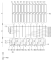
선택 회로(SC)는 데이터 라인들(DL1 내지 DLn)과 구동칩(DIC) 사이에 배치될 수 있다. 선택 회로(SC)는 제1 구간동안 데이터 라인들(DL1 내지 DLn) 중 일부(예를 들어, 제1 그룹)를 구동칩(DIC)에 전기적으로 연결시키고, 제2 구간동안 데이터 라인들(DL1 내지 DLn) 중 일부(예를 들어, 제2 그룹)를 구동칩(DIC)에 전기적으로 연결시킨다. 본 발명의 일 예로, 제1 그룹은 데이터 라인들(DL1 내지 DLn) 중 홀수번째 데이터 라인들을 포함할 수 있고, 제2 그룹은 데이터 라인들(DL1 내지 DLn) 중 짝수번째 데이터 라인들을 포함할 수 있다.The selection circuit (SC) may be disposed between the data lines (DL1 to DLn) and the driving chip (DIC). The selection circuit (SC) electrically connects some of the data lines (DL1 to DLn) (e.g., the first group) to the driving chip (DIC) during the first period, and connects the data lines (DL1) to the driving chip (DIC) during the second period. to DLn) (for example, a second group) are electrically connected to the driving chip (DIC). As an example of the present invention, the first group may include odd-numbered data lines among the data lines DL1 to DLn, and the second group may include even-numbered data lines among the data lines DL1 to DLn. there is.
본 발명의 일 예로, 선택 회로(SC)는 비표시 영역(NDA)에 배치될 수 있다. 특히, 선택 회로(SC)는 제3 영역(A3) 내에 배치되어 구동칩(DIC)과 함께 표시 모듈(DM)의 배면에 위치할 수 있다. 이 경우, 선택 회로(SC)가 제1 영역(A1) 내에 배치되는 표시패널에 비해, 제1 영역(A1)에서의 비표시 영역(NDA)의 면적이 감소될 수 있고, 그 결과 네로우 베젤(narrow bezel)을 가진 표시 장치(DD)가 구현될 수 있다.As an example of the present invention, the selection circuit (SC) may be disposed in the non-display area (NDA). In particular, the selection circuit SC may be disposed in the third area A3 and located on the back of the display module DM along with the driving chip DIC. In this case, compared to a display panel in which the selection circuit (SC) is disposed in the first area (A1), the area of the non-display area (NDA) in the first area (A1) may be reduced, resulting in a narrow bezel. A display device (DD) with a narrow bezel may be implemented.
선택 회로(SC)와 데이터 라인들(DL1 내지 DLn)은 팬아웃 라인들(POL)을 통해 전기적으로 연결될 수 있다. 팬아웃 라인들(POL)은 제2 영역(A2)에 배치되고, 제1 영역(A1)에서 데이터 라인들(DL1 내지 DLn)과 접속되며, 제3 영역(A3)에서 선택 회로(SC)와 접속될 수 있다.The selection circuit (SC) and the data lines (DL1 to DLn) may be electrically connected through fan-out lines (POL). The fan-out lines (POL) are arranged in the second area (A2), connected to the data lines (DL1 to DLn) in the first area (A1), and connected to the selection circuit (SC) in the third area (A3). can be connected.
도 3은 본 발명의 일 실시예에 따른 화소의 회로도이다. 도 3은 도 2에 도시된 복수의 화소들(PX) 중 하나의 화소(PX)의 등가 회로도를 도시하였다.Figure 3 is a circuit diagram of a pixel according to an embodiment of the present invention. FIG. 3 shows an equivalent circuit diagram of one pixel (PX) among the plurality of pixels (PX) shown in FIG. 2.
도 3을 참조하면, 화소(PX)는 발광 소자(ED) 및 화소 구동 회로(PDC)를 포함할 수 있다. Referring to FIG. 3 , the pixel PX may include a light emitting element (ED) and a pixel driving circuit (PDC).
화소 구동 회로(PDC)는 복수의 트랜지스터들(T1 내지 T7) 및 스토리지 커패시터(Cst)를 포함할 수 있다. 화소 구동 회로(PDC)는 신호 라인들(SL1, SL2, SL3, SL4, EL, DL), 제1 초기화 전압 라인(VL1), 제2 초기화 전압 라인(VL2)(또는, 애노드 초기화 전압 라인), 제1 전원 라인(PL1)에 전기적으로 연결될 수 있다. 일 실시예로, 상술한 라인들 중 적어도 어느 하나, 예컨대, 제1 전원 라인(PL1)은 이웃하는 화소들(PX)과 공유될 수 있다.The pixel driving circuit (PDC) may include a plurality of transistors (T1 to T7) and a storage capacitor (Cst). The pixel driving circuit (PDC) includes signal lines (SL1, SL2, SL3, SL4, EL, DL), a first initialization voltage line (VL1), a second initialization voltage line (VL2) (or an anode initialization voltage line), It may be electrically connected to the first power line PL1. In one embodiment, at least one of the above-described lines, for example, the first power line PL1, may be shared with neighboring pixels PX.
복수의 트랜지스터들(T1 내지 T7)은 구동 트랜지스터(T1)(또는 제1 트랜지스터), 스위칭 트랜지스터(T2)(또는 제2 트랜지스터), 보상 트랜지스터(T3)(또는 제3 트랜지스터), 제1 초기화 트랜지스터(T4)(또는 제4 트랜지스터), 제1 제어 트랜지스터(T5)(또는 제5 트랜지스터), 제2 제어 트랜지스터(T6)(또는 제6 트랜지스터) 및 제2 초기화 트랜지스터(T7)(또는 제7 트랜지스터)를 포함할 수 있다.The plurality of transistors T1 to T7 include a driving transistor T1 (or first transistor), a switching transistor T2 (or second transistor), a compensation transistor T3 (or third transistor), and a first initialization transistor. (T4) (or fourth transistor), first control transistor (T5) (or fifth transistor), second control transistor (T6) (or sixth transistor), and second initialization transistor (T7) (or seventh transistor) ) may include.
발광 소자(ED)는 제1 전극(예를 들어, 애노드 전극) 및 제2 전극(CE)(예를 들어, 캐소드 전극)을 포함할 수 있다. 발광 소자(ED)의 상기 제1 전극은 제2 제어 트랜지스터(T6)을 매개로 구동 트랜지스터(T1)에 연결되어 구동 전류(Id)를 제공받고, 제2 전극(CE)은 제2 전원 라인(PL2)에 연결된 제2 구동 전압(ELVSS)을 제공받을 수 있다. 발광 소자(ED)는 구동 전류(Id)에 상응하는 휘도의 광을 생성할 수 있다. 일 실시예로, 발광 소자(ED)의 제2 전극(CE)은 화소들(PX)에 공통적으로 연결되는 공통 전극으로 제공될 수 있다.The light emitting device ED may include a first electrode (eg, an anode electrode) and a second electrode (CE) (eg, a cathode electrode). The first electrode of the light emitting element (ED) is connected to the driving transistor (T1) via the second control transistor (T6) to receive a driving current (Id), and the second electrode (CE) is connected to the second power line ( A second driving voltage (ELVSS) connected to PL2) may be provided. The light emitting element ED may generate light with a brightness corresponding to the driving current Id. In one embodiment, the second electrode CE of the light emitting device ED may be provided as a common electrode commonly connected to the pixels PX.
복수의 트랜지스터들(T1 내지 T7) 중 일부는 NMOS(n-channel MOSFET)로 구비되고, 나머지는 PMOS(p-channel MOSFET)으로 구비될 수 있다. 예를 들어, 복수의 트랜지스터들(T1 내지 T7) 중 보상 트랜지스터(T3) 및 제1 초기화 트랜지스터(T4)는 NMOS(n-channel MOSFET)로 구비되며, 나머지는 PMOS(p-channel MOSFET)으로 구비될 수 있다.Some of the plurality of transistors (T1 to T7) may be provided as n-channel MOSFETs (NMOS), and others may be provided as p-channel MOSFETs (PMOS). For example, among the plurality of transistors T1 to T7, the compensation transistor T3 and the first initialization transistor T4 are provided as n-channel MOSFETs (NMOS), and the rest are provided as p-channel MOSFETs (PMOS). It can be.
다른 실시예로, 복수의 트랜지스터들(T1 내지 T7) 중 보상 트랜지스터(T3), 제1 초기화 트랜지스터(T4) 및 제2 초기화 트랜지스터(T7)은 NMOS로 구비되며, 나머지는 PMOS으로 구비될 수 있다. 또는, 복수의 트랜지스터들(T1 내지 T7) 중 하나만 NMOS로 구비되고 나머지는 PMOS로 구비될 수 있다. 또는, 복수의 트랜지스터들(T1 내지 T7) 모두 NMOS로 구비되거나, 모두 PMOS로 구비될 수 있다.In another embodiment, among the plurality of transistors T1 to T7, the compensation transistor T3, the first initialization transistor T4, and the second initialization transistor T7 may be NMOS, and the rest may be PMOS. . Alternatively, only one of the plurality of transistors T1 to T7 may be equipped with NMOS and the remaining transistors may be equipped with PMOS. Alternatively, all of the plurality of transistors T1 to T7 may be NMOS, or all may be PMOS.
신호 라인들은 제1 스캔신호(SS1)를 전달하는 제1 스캔 라인(SL1), 제2 스캔신호(SS2)을 전달하는 제2 스캔 라인(SL2), 제1 초기화 트랜지스터(T4)에 제3 스캔신호(SS3)를 전달하는 제3 스캔 라인(SL3), 제1 제어 트랜지스터(T5) 및 제2 제어 트랜지스터(T6)에 발광제어신호(En)를 전달하는 발광제어 라인(EL), 제2 초기화 트랜지스터(T7)에 제4 스캔신호(SS4)를 전달하는 제4 스캔 라인(SL4), 및 제1 스캔 라인(SL1)과 교차하며 데이터 신호(Dm)를 전달하는 데이터 라인(DL)을 포함할 수 있다.The signal lines include a first scan line (SL1) transmitting the first scan signal (SS1), a second scan line (SL2) transmitting the second scan signal (SS2), and a third scan line to the first initialization transistor (T4). A third scan line (SL3) transmitting the signal SS3, an emission control line (EL) transmitting the emission control signal (En) to the first control transistor (T5) and the second control transistor (T6), and a second initialization It may include a fourth scan line (SL4) that transmits the fourth scan signal (SS4) to the transistor (T7), and a data line (DL) that intersects the first scan line (SL1) and transmits the data signal (Dm). You can.
제1 전원 라인(PL1)은 구동 트랜지스터(T1)에 제1 구동 전압(ELVDD)을 전달하며, 제1 초기화 전압 라인(VL1)은 구동 트랜지스터(T1)의 게이트 전극 및 발광 소자(ED)의 제1 전극을 초기화하는 제1 초기화 전압(Vint)을 전달할 수 있다.The first power line (PL1) delivers the first driving voltage (ELVDD) to the driving transistor (T1), and the first initialization voltage line (VL1) transmits the gate electrode of the driving transistor (T1) and the first driving voltage (ELVDD) of the light emitting device (ED). 1 The first initialization voltage (Vint) that initializes the electrode may be transmitted.
구동 트랜지스터(T1)의 게이트 전극은 스토리지 커패시터(Cst)와 연결되고, 구동 트랜지스터(T1)의 제1 전극(또는 소오스 전극)은 제1 제어 트랜지스터(T5)를 경유하여 제1 전원 라인(PL1)에 연결되며, 구동 트랜지스터(T1)의 제2 전극(또는 드레인 전극)은 제2 제어 트랜지스터(T6)를 경유하여 발광 소자(ED)의 제1 전극과 전기적으로 연결될 수 있다. 구동 트랜지스터(T1)는 스위칭 트랜지스터(T2)의 스위칭 동작에 따라 데이터 신호(Dm)를 전달받아 발광 소자(ED)에 구동 전류(Id)를 공급할 수 있다.The gate electrode of the driving transistor T1 is connected to the storage capacitor Cst, and the first electrode (or source electrode) of the driving transistor T1 is connected to the first power line PL1 via the first control transistor T5. and the second electrode (or drain electrode) of the driving transistor T1 may be electrically connected to the first electrode of the light emitting device ED via the second control transistor T6. The driving transistor T1 may receive the data signal Dm according to the switching operation of the switching transistor T2 and supply the driving current Id to the light emitting device ED.
스위칭 트랜지스터(T2)의 게이트 전극은 제1 스캔신호(SS1)를 전달하는 제1 스캔 라인(SL1)에 연결되고, 스위칭 트랜지스터(T2)의 제1 전극은 데이터 라인(DL)에 연결되며, 스위칭 트랜지스터(T2)의 제2 전극은 구동 트랜지스터(T1)의 제1 전극에 연결될 수 있다. 스위칭 트랜지스터(T2)는 제1 스캔 라인(SL1)을 통해 전달받은 제1 스캔신호(SS1)에 따라 턴-온되어 데이터 라인(DL)으로부터 전달된 데이터신호(Dm)를 구동 트랜지스터(T1)의 제1 전극으로 전달하는 스위칭 동작을 수행할 수 있다.The gate electrode of the switching transistor (T2) is connected to the first scan line (SL1) transmitting the first scan signal (SS1), the first electrode of the switching transistor (T2) is connected to the data line (DL), and the switching The second electrode of the transistor T2 may be connected to the first electrode of the driving transistor T1. The switching transistor T2 is turned on according to the first scan signal SS1 received through the first scan line SL1 and transmits the data signal Dm transmitted from the data line DL to the driving transistor T1. A switching operation that transmits data to the first electrode can be performed.
보상 트랜지스터(T3)의 게이트 전극은 제2 스캔 라인(SL2)에 연결된다. 보상 트랜지스터(T3)의 제1 전극은 구동 트랜지스터(T1)의 제2 전극에 연결되고, 보상 트랜지스터(T3)의 제2 전극은 스토리지 커패시터(Cst)의 제1 전극(CSE1) 및 구동 트랜지스터(T1)의 게이트 전극에 연결될 수 있다. 보상 트랜지스터(T3)는 제2 스캔 라인(SL2)을 통해 전달받은 제2 스캔신호(SS2)에 따라 턴-온되어 구동 트랜지스터(T1)의 게이트 전극과 제2 전극을 전기적으로 연결하여 구동 트랜지스터(T1)를 다이오드 연결시킬 수 있다.The gate electrode of the compensation transistor T3 is connected to the second scan line SL2. The first electrode of the compensation transistor (T3) is connected to the second electrode of the driving transistor (T1), and the second electrode of the compensation transistor (T3) is connected to the first electrode (CSE1) of the storage capacitor (Cst) and the driving transistor (T1). ) can be connected to the gate electrode. The compensation transistor T3 is turned on according to the second scan signal SS2 received through the second scan line SL2 and electrically connects the gate electrode and the second electrode of the driving transistor T1 to operate the driving transistor ( T1) can be connected to a diode.
제1 초기화 트랜지스터(T4)의 게이트 전극은 제3 스캔 라인(SL3)에 연결될 수 있다. 제1 초기화 트랜지스터(T4)의 제1 전극은 제1 초기화 전압 라인(VL1)에 연결되고, 제1 초기화 트랜지스터(T4)의 제2 전극은 스토리지 커패시터(Cst)의 제1 전극(CSE1), 보상 트랜지스터(T3)의 제2 전극 및 구동 트랜지스터(T1)의 게이트 전극에 연결될 수 있다. 제1 초기화 트랜지스터(T4)는 제3 스캔 라인(SL3)을 통해 전달받은 제3 스캔신호(SS3)에 따라 턴-온되어 제1 초기화 전압(Vint)을 구동 트랜지스터(T1)의 게이트 전극에 전달하여 구동 트랜지스터(T1)의 게이트 전극을 제1 초기화 전압(Vint)으로 초기화시키는 초기화 동작을 수행할 수 있다.The gate electrode of the first initialization transistor T4 may be connected to the third scan line SL3. The first electrode of the first initialization transistor T4 is connected to the first initialization voltage line VL1, and the second electrode of the first initialization transistor T4 is connected to the first electrode CSE1 of the storage capacitor Cst, compensation It may be connected to the second electrode of the transistor T3 and the gate electrode of the driving transistor T1. The first initialization transistor T4 is turned on according to the third scan signal SS3 received through the third scan line SL3 and transmits the first initialization voltage Vint to the gate electrode of the driving transistor T1. Thus, an initialization operation can be performed to initialize the gate electrode of the driving transistor T1 to the first initialization voltage Vint.
제1 제어 트랜지스터(T5)의 게이트 전극은 발광제어 라인(EL)에 연결되며, 제1 제어 트랜지스터(T5)의 제1 전극은 제1 전원 라인(PL1)과 연결되고, 제1 제어 트랜지스터(T5)의 제2 전극은 구동 트랜지스터(T1)의 제1 전극 및 스위칭 트랜지스터(T2)의 제2 전극과 연결될 수 있다.The gate electrode of the first control transistor T5 is connected to the light emission control line EL, the first electrode of the first control transistor T5 is connected to the first power line PL1, and the first control transistor T5 ) may be connected to the first electrode of the driving transistor (T1) and the second electrode of the switching transistor (T2).
제2 제어 트랜지스터(T6)의 게이트 전극은 발광제어 라인(EL)에 연결되고, 제2 제어 트랜지스터(T6)의 제1 전극은 구동 트랜지스터(T1)의 제2 전극 및 보상 트랜지스터(T3)의 제1 전극에 연결된다. 제2 제어 트랜지스터(T6)의 제2 전극은 발광 소자(ED)의 제1 전극에 연결된다.The gate electrode of the second control transistor T6 is connected to the light emission control line EL, and the first electrode of the second control transistor T6 is connected to the second electrode of the driving transistor T1 and the first electrode of the compensation transistor T3. 1 is connected to the electrode. The second electrode of the second control transistor T6 is connected to the first electrode of the light emitting element ED.
제1 제어 트랜지스터(T5) 및 제2 제어 트랜지스터(T6)는 발광제어 라인(EL)을 통해 전달받은 발광제어신호(En)에 응답하여 동시에 턴-온되어, 제1 구동 전압(ELVDD)이 발광 소자(ED)에 전달되어 발광 소자(ED)에 구동 전류(Id)가 흐르도록 한다. 대안적으로, 제1 제어 트랜지스터(T5) 및 제2 제어 트랜지스터(T6)는 서로 다른 발광제어 라인에 각각 연결될 수 있다.The first control transistor (T5) and the second control transistor (T6) are simultaneously turned on in response to the light emission control signal (En) received through the light emission control line (EL), so that the first driving voltage (ELVDD) emits light. It is transmitted to the element ED so that the driving current Id flows in the light emitting element ED. Alternatively, the first control transistor T5 and the second control transistor T6 may each be connected to different emission control lines.
제2 초기화 트랜지스터(T7)의 게이트 전극은 제4 스캔 라인(SL4)에 연결되고, 제2 초기화 트랜지스터(T7)의 제1 전극은 제2 초기화 전압 라인(VL2)에 연결되어 제2 초기화 전압(Aint)을 제공받을 수 있다. 제2 초기화 트랜지스터(T7)의 제2 전극은 제2 제어 트랜지스터(T6)의 제2 전극 및 발광 소자(ED)의 제1 전극에 연결된다. 제2 초기화 트랜지스터(T7)는 제4 스캔 라인(SL4)을 통해 전달받은 제4 스캔신호(SS4)에 따라 턴-온되어 발광 소자(ED)의 제1 전극을 제2 초기화 전압(Aint)으로 초기화시킨다.The gate electrode of the second initialization transistor T7 is connected to the fourth scan line SL4, and the first electrode of the second initialization transistor T7 is connected to the second initialization voltage line VL2 to provide a second initialization voltage ( Aint) can be provided. The second electrode of the second initialization transistor T7 is connected to the second electrode of the second control transistor T6 and the first electrode of the light emitting device ED. The second initialization transistor T7 is turned on according to the fourth scan signal SS4 received through the fourth scan line SL4 to set the first electrode of the light emitting device ED to the second initialization voltage Aint. Initialize.
다른 실시예로, 제2 초기화 트랜지스터(T7)는 발광제어 라인(EL)에 연결되어 발광제어신호(En)에 따라 구동될 수 있다. 한편, 각 트랜지스터의 제1 및 제2 전극들은 트랜지스터의 종류(p-type or n-type)에 따라 그 위치가 서로 바뀔 수 있다.In another embodiment, the second initialization transistor T7 may be connected to the emission control line EL and driven according to the emission control signal En. Meanwhile, the positions of the first and second electrodes of each transistor may change depending on the type of transistor (p-type or n-type).
스토리지 커패시터(Cst)는 제1 전극(CSE1)과 제2 전극(CSE2)를 포함할 수 있다. 스토리지 커패시터(Cst)의 제1 전극(CSE1)은 구동 트랜지스터(T1)의 게이트 전극과 연결되며, 스토리지 커패시터(Cst)의 제2 전극(CSE2)은 제1 전원 라인(PL1)과 연결된다. 스토리지 커패시터(Cst)는 구동 트랜지스터(T1)의 게이트 전극의 전위와 제1 구동 전압(ELVDD) 차이에 대응하는 전하가 저장될 수 있다.The storage capacitor Cst may include a first electrode CSE1 and a second electrode CSE2. The first electrode (CSE1) of the storage capacitor (Cst) is connected to the gate electrode of the driving transistor (T1), and the second electrode (CSE2) of the storage capacitor (Cst) is connected to the first power line (PL1). The storage capacitor Cst may store a charge corresponding to the difference between the potential of the gate electrode of the driving transistor T1 and the first driving voltage ELVDD.
일 실시예에 따른 각 화소(PX)의 구체적 동작은 다음과 같다.The specific operation of each pixel (PX) according to one embodiment is as follows.
초기화 기간 동안, 제3 스캔 라인(SL3)을 통해 제3 스캔신호(SS3)가 공급되면, 제3 스캔신호(SS3)에 대응하여 제1 초기화 트랜지스터(T4)가 턴-온(Turn on)되며, 제1 초기화 전압 라인(VL1)으로부터 공급되는 제1 초기화 전압(Vint)에 의해 구동 트랜지스터(T1)가 초기화된다.During the initialization period, when the third scan signal SS3 is supplied through the third scan line SL3, the first initialization transistor T4 is turned on in response to the third scan signal SS3. , the driving transistor T1 is initialized by the first initialization voltage Vint supplied from the first initialization voltage line VL1.
데이터 프로그래밍 기간 동안, 제1 스캔 라인(SL1) 및 제2 스캔 라인(SL2)을 통해 제1 스캔신호(SS1) 및 제2 스캔신호(SS2)가 공급되면, 제1 스캔신호(SS) 및 제2 스캔신호(SS2)에 대응하여 스위칭 트랜지스터(T2) 및 보상 트랜지스터(T3)가 턴-온된다. 이 때, 구동 트랜지스터(T1)는 턴-온된 보상 트랜지스터(T3)에 의해 다이오드 연결되고, 순방향으로 바이어스 된다.During the data programming period, when the first scan signal (SS1) and the second scan signal (SS2) are supplied through the first scan line (SL1) and the second scan line (SL2), the first scan signal (SS) and the second scan signal (SS2) are 2 The switching transistor (T2) and compensation transistor (T3) are turned on in response to the scan signal (SS2). At this time, the driving transistor T1 is diode-connected and forward biased by the turned-on compensation transistor T3.
그러면, 데이터 라인(DL)으로부터 공급된 데이터 신호(Dm)에서 구동 트랜지스터(T1)의 문턱 전압(Threshold voltage, Vth)만큼 감소한 보상 전압(Dm+Vth, Vth는 (-)의 값)이 구동 트랜지스터(T1)의 게이트 전극에 인가된다.Then, the compensation voltage (Dm+Vth, Vth is a (-) value) reduced by the threshold voltage (Vth) of the driving transistor (T1) from the data signal (Dm) supplied from the data line (DL) is applied to the driving transistor. It is applied to the gate electrode of (T1).
스토리지 커패시터(Cst)의 양단에는 제1 구동 전압(ELVDD)과 보상 전압(Dm+Vth)이 인가되고, 스토리지 커패시터(Cst)에는 양단 전압 차에 대응하는 전하가 저장된다.A first driving voltage (ELVDD) and a compensation voltage (Dm+Vth) are applied to both ends of the storage capacitor (Cst), and a charge corresponding to the voltage difference between both ends is stored in the storage capacitor (Cst).
발광 기간 동안, 발광제어 라인(EL)으로부터 공급되는 발광제어신호(En)에 의해 제1 제어 트랜지스터(T5) 및 제2 제어 트랜지스터(T6)가 턴-온된다. 구동 트랜지스터(T1)의 게이트 전극의 전압과 제1 구동 전압(ELVDD) 간의 전압차에 따르는 구동 전류(Id)가 발생하고, 제2 제어 트랜지스터(T6)를 통해 구동 전류(Id)가 발광 소자(ED)에 공급된다.During the light emission period, the first control transistor T5 and the second control transistor T6 are turned on by the light emission control signal En supplied from the light emission control line EL. A driving current (Id) is generated according to the voltage difference between the voltage of the gate electrode of the driving transistor (T1) and the first driving voltage (ELVDD), and the driving current (Id) is transmitted through the second control transistor (T6) to the light emitting device ( ED).
본 실시예에서는 복수의 트랜지스터들(T1 내지 T7) 중 적어도 하나는 산화물을 포함하는 반도체층을 포함하며, 나머지는 실리콘을 포함하는 반도체층을 포함하고 있다. 구체적으로, 디스플레이 장치의 밝기에 직접적으로 영향을 미치는 구동 트랜지스터(T1)의 경우 높은 신뢰성을 갖는 다결정 실리콘으로 구성된 반도체층을 포함하도록 구성하며, 이를 통해 고해상도의 디스플레이 장치를 구현할 수 있다. 한편, 산화물 반도체는 높은 캐리어 이동도(high carrier mobility) 및 낮은 누설전류를 가지므로, 구동 시간이 길더라도 전압 강하가 크지 않다. 즉, 저주파 구동 시에도 전압 강하에 따른 화상의 색상 변화가 크지 않으므로, 저주파 구동이 가능하다.In this embodiment, at least one of the plurality of transistors T1 to T7 includes a semiconductor layer containing oxide, and the remaining transistors include a semiconductor layer containing silicon. Specifically, the driving transistor T1, which directly affects the brightness of the display device, is configured to include a semiconductor layer made of highly reliable polycrystalline silicon, through which a high-resolution display device can be implemented. Meanwhile, oxide semiconductors have high carrier mobility and low leakage current, so the voltage drop is not large even if the driving time is long. That is, even during low-frequency driving, the color change of the image due to voltage drop is not significant, so low-frequency driving is possible.
이와 같이 산화물 반도체의 경우 누설전류가 적은 이점을 갖기에, 보상 트랜지스터(T3) 및 제1 초기화 트랜지스터(T4) 중 적어도 하나를 산화물 반도체로 채용하여 구동 트랜지스터(T1)의 게이트 전극으로 흘러갈 수 있는 누설전류를 방지하는 동시에 소비전력을 줄일 수 있다.In this way, since the oxide semiconductor has the advantage of low leakage current, at least one of the compensation transistor (T3) and the first initialization transistor (T4) is adopted as an oxide semiconductor, so that the leakage current can flow to the gate electrode of the driving transistor (T1). It can prevent leakage current and reduce power consumption.
도 4는 도 1c에 도시된 표시 모듈의 일부 영역을 나타낸 단면도이다.FIG. 4 is a cross-sectional view showing a partial area of the display module shown in FIG. 1C.
도 4를 참조하면, 표시 모듈(DM)은 표시패널(DP) 및 표시패널(DP) 위에 직접 배치된 입력 감지층(ISP)를 포함할 수 있다. 표시패널(DP)은 베이스층(BL), 회로 소자층(DP-CL), 발광 소자층(DP-EL), 및 봉지층(TFE)을 포함할 수 있다. Referring to FIG. 4 , the display module DM may include a display panel DP and an input sensing layer (ISP) disposed directly on the display panel DP. The display panel (DP) may include a base layer (BL), a circuit element layer (DP-CL), a light emitting element layer (DP-EL), and an encapsulation layer (TFE).
베이스층(BL)은 회로 소자층(DP-CL)이 배치되는 베이스 면을 제공할 수 있다. 회로 소자층(DP-CL)은 베이스층(BL) 위에 배치될 수 있다. 회로 소자층(DP-CL)은 절연층, 반도체 패턴, 도전 패턴, 및 신호 라인 등을 포함할 수 있다. 코팅, 증착 등의 방식으로 절연층, 반도체층, 및 도전층이 베이스층(BL) 위에 형성되고, 이후, 복수 회의 포토리소그래피 공정을 통해 절연층, 반도체층, 및 도전층이 선택적으로 패터닝될 수 있다. 이후, 회로 소자층(DP-CL)에 포함된 반도체 패턴, 도전 패턴, 및 신호 라인이 형성될 수 있다. The base layer BL may provide a base surface on which the circuit element layer DP-CL is disposed. The circuit element layer (DP-CL) may be disposed on the base layer (BL). The circuit element layer (DP-CL) may include an insulating layer, a semiconductor pattern, a conductive pattern, and a signal line. An insulating layer, a semiconductor layer, and a conductive layer are formed on the base layer (BL) by coating, deposition, etc., and then the insulating layer, a semiconductor layer, and a conductive layer can be selectively patterned through multiple photolithography processes. there is. Thereafter, semiconductor patterns, conductive patterns, and signal lines included in the circuit element layer (DP-CL) may be formed.
베이스층(BL)의 상면에 적어도 하나의 무기층이 형성된다. 본 실시예에서 표시패널(DP)은 2개의 버퍼층(BFL1, BFL2)(즉, 제1 및 제2 버퍼층)을 포함하는 것으로 도시되었다. 제1 및 제2 버퍼층(BFL1, BFL2)은 베이스층(BL)과 반도체 패턴 사이의 결합력을 향상시킬 수 있다. 제1 및 제2 버퍼층(BFL1, BFL2)은 실리콘옥사이드층 및 실리콘나이트라이드층을 포함할 수 있으며, 실리콘옥사이드층과 실리콘나이트라이드층은 교대로 적층될 수 있다.At least one inorganic layer is formed on the upper surface of the base layer BL. In this embodiment, the display panel DP is shown as including two buffer layers BFL1 and BFL2 (ie, first and second buffer layers). The first and second buffer layers BFL1 and BFL2 can improve the bonding force between the base layer BL and the semiconductor pattern. The first and second buffer layers BFL1 and BFL2 may include a silicon oxide layer and a silicon nitride layer, and the silicon oxide layer and the silicon nitride layer may be alternately stacked.
제1 반도체 패턴은 제2 버퍼층(BFL2) 위에 배치될 수 있다. 제1 반도체 패턴은 폴리실리콘을 포함할 수 있다. 그러나 이에 제한되지 않고, 반도체 패턴은 비정질실리콘 또는 금속 산화물을 포함할 수도 있다.The first semiconductor pattern may be disposed on the second buffer layer BFL2. The first semiconductor pattern may include polysilicon. However, the pattern is not limited thereto, and the semiconductor pattern may include amorphous silicon or metal oxide.
도 4는 일부의 제1 반도체 패턴을 도시한 것일 뿐이고, 다른 영역에 제1 반도체 패턴이 더 배치될 수 있다. 제1 반도체 패턴은 화소들에 걸쳐 특정한 규칙으로 배열될 수 있다. 제1 반도체 패턴은 도핑 여부에 따라 전기적 성질이 다를 수 있다. 제1 반도체 패턴은 전도율이 높은 제1 영역과 전도율이 낮은 제2 영역을 포함할 수 있다. 제1 영역은 N형 도판트 또는 P형 도판트로 도핑될 수 있다. P타입의 트랜지스터는 P형 도판트로 도핑된 도핑영역을 포함한다. 제2 영역은 비-도핑영역이거나, 제1 영역 대비 낮은 농도로 도핑될 수 있다.FIG. 4 only illustrates a portion of the first semiconductor pattern, and additional first semiconductor patterns may be disposed in other areas. The first semiconductor pattern may be arranged in a specific rule across the pixels. The first semiconductor pattern may have different electrical properties depending on whether or not it is doped. The first semiconductor pattern may include a first region with high conductivity and a second region with low conductivity. The first region may be doped with an N-type dopant or a P-type dopant. A P-type transistor includes a doped region doped with a P-type dopant. The second region may be a non-doped region or may be doped at a lower concentration than the first region.
제1 영역의 전도성은 제2 영역보다 크고, 실질적으로 전극 또는 신호 라인의 역할을 갖는다. 제2 영역은 실질적으로 트랜지스터의 활성화 영역(또는 채널 영역)에 해당할 수 있다. 다시 말해, 제1 반도체 패턴의 일부분은 트랜지스터의 채널 영역일 수 있고, 다른 일부분은 트랜지스터의 소스 영역 또는 드레인 영역일 수 있다. The conductivity of the first region is greater than that of the second region, and substantially serves as an electrode or signal line. The second area may substantially correspond to the active area (or channel area) of the transistor. In other words, a portion of the first semiconductor pattern may be a channel region of the transistor, and another portion may be a source region or drain region of the transistor.
도 4에는 발광 소자(ED) 및 화소 구동 회로(PDC, 도 3 참조)의 보상 트랜지스터(T3) 및 제2 제어 트랜지스터(T6)가 예시적으로 도시되었다. In FIG. 4 , the compensation transistor T3 and the second control transistor T6 of the light emitting device (ED) and the pixel driving circuit (PDC, see FIG. 3 ) are shown as examples.
제2 제어 트랜지스터(T6)의 소스 영역(SE1), 채널 영역(AC1), 및 드레인 영역(DE1)이 제1 반도체 패턴으로부터 형성될 수 있다. 소스 영역(SE1) 및 드레인 영역(DE1)은 단면 상에서 채널 영역(AC1)으로부터 서로 반대 방향에 연장될 수 있다.The source region (SE1), channel region (AC1), and drain region (DE1) of the second control transistor (T6) may be formed from the first semiconductor pattern. The source region SE1 and the drain region DE1 may extend in opposite directions from the channel region AC1 in a cross-section.
제1 절연층(10)은 제2 버퍼층(BFL2) 위에 배치될 수 있다. 제1 절연층(10)은 복수 개의 화소들에 공통으로 중첩하며, 제1 반도체 패턴을 커버할 수 있다. 제1 절연층(10)은 무기층 및/또는 유기층일 수 있으며, 단층 또는 다층 구조를 가질 수 있다. 제1 절연층(10)은 알루미늄옥사이드, 티타늄옥사이드, 실리콘옥사이드, 실리콘나이트라이드, 실리콘옥시나이트라이드, 지르코늄옥사이드, 및 하프늄옥사이드 중 적어도 하나를 포함할 수 있다. 본 실시예에서 제1 절연층(10)은 단층의 실리콘옥사이드층일 수 있다. 제1 절연층(10)뿐만 아니라 후술하는 회로 소자층(DP-CL)의 절연층은 무기층 및/또는 유기층일 있으며, 단층 또는 다층 구조를 가질 수 있다. 무기층은 상술한 물질 중 적어도 하나를 포함할 수 있으나, 이에 제한되는 것은 아니다.The first insulating
제2 제어 트랜지스터(T6)의 게이트 전극(GT1)은 제1 절연층(10) 위에 배치된다. 게이트 전극(GT1)은 금속 패턴의 일부분일 수 있다. 게이트 전극(GT1)은 채널 영역(AC1)에 중첩한다. 제1 반도체 패턴을 도핑하는 공정에서 게이트 전극(GT1)은 마스크로써 기능할 수 있다. The gate electrode (GT1) of the second control transistor (T6) is disposed on the first insulating layer (10). The gate electrode GT1 may be part of a metal pattern. The gate electrode GT1 overlaps the channel area AC1. In the process of doping the first semiconductor pattern, the gate electrode GT1 may function as a mask.
제2 절연층(20)은 제1 절연층(10) 위에 배치되며, 게이트 전극(GT1)을 커버할 수 있다. 제2 절연층(20)은 화소들에 공통으로 중첩할 수 있다. 제2 절연층(20)은 무기층 및/또는 유기층일 수 있으며, 단층 또는 다층 구조를 가질 수 있다. 본 실시예에서 제2 절연층(20)은 단층의 실리콘옥사이드층일 수 있다.The second insulating
제2 제어 트랜지스터(T6)의 상부 게이트 전극(UGT)은 제2 절연층(20) 위에 배치된다. 상부 게이트 전극(UGT)은 금속 패턴의 일부분일 수 있다. 상부 게이트 전극(UGT)은 제2 제어 트랜지스터(T6)의 게이트 전극(GT1)에 중첩한다.The upper gate electrode (UGT) of the second control transistor (T6) is disposed on the second insulating layer (20). The upper gate electrode (UGT) may be part of a metal pattern. The upper gate electrode (UGT) overlaps the gate electrode (GT1) of the second control transistor (T6).
제3 절연층(30)은 제2 절연층(20) 위에 배치될 수 있다. 제3 절연층(30)은 복수 개의 화소들에 공통으로 중첩하며, 상부 게이트 전극(UGT)을 커버할 수 있다. 제3 절연층(30)은 단층 또는 다층 구조를 가질 수 있다. 예를 들어, 제3 절연층(30)은 실리콘옥사이드층 및 실리콘나이트라이드층을 포함하는 다층 구조를 가질 수 있다. 제2 절연층(20)과 제3 절연층(30) 사이에는 배면 금속층(BML)이 배치될 수 있다. 배면 금속층(BML)은 정전압 또는 신호를 인가 받을 수 있다. 배면 금속층(BML)은 제2 제어 트랜지스터(T6)의 상부 게이트 전극(UGT)과 동일 층에 배치될 수 있다.The third insulating
제2 반도체 패턴은 제3 절연층(30) 위에 배치될 수 있다. 제2 반도체 패턴은 산화물 반도체를 포함할 수 있다. 산화물 반도체는 금속 산화물이 환원되었는지의 여부에 따라 구분되는 복수 개의 영역들을 포함할 수 있다. 금속 산화물이 환원된 영역(이하, 환원 영역)은 그렇지 않은 영역(이하, 비환원 영역) 대비 큰 전도성을 갖는다. 환원 영역은 실질적으로 트랜지스터의 소스 영역/드레인 영역 또는 신호라인의 역할을 갖는다. 비환원 영역이 실질적으로 트랜지스터의 활성화 영역(또는 채널 영역)에 해당한다. 다시 말해, 제2 반도체 패턴의 일부분은 트랜지스터의 패널 영역일 수 있고, 다른 일부분은 트랜지스터의 소스 영역/드레인 영역일 수 있으며, 또 다른 일부분은 신호 전달 영역일 수 있다.The second semiconductor pattern may be disposed on the third insulating
보상 트랜지스터(T3)의 소스 영역(SE2), 채널 영역(AC2), 및 드레인 영역(DE2)은 제2 반도체 패턴으로부터 형성될 수 있다. 소스 영역(SE2) 및 드레인 영역(DE2)은 단면 상에서 채널 영역(AC2)로부터 서로 반대 방향으로 연장될 수 있다.The source region (SE2), channel region (AC2), and drain region (DE2) of the compensation transistor T3 may be formed from the second semiconductor pattern. The source region SE2 and the drain region DE2 may extend in opposite directions from the channel region AC2 in a cross-section.
제4 절연층(40)은 제3 절연층(30) 위에 배치될 수 있다. 제4 절연층(40)은 복수 개의 화소들에 공통으로 중첩하며, 제2 반도체 패턴을 커버할 수 있다. 제4 절연층(40)은 알루미늄옥사이드, 티타늄옥사이드, 실리콘옥사이드, 실리콘나이트라이드, 실리콘옥시나이트라이드, 지르코늄옥사이드, 및 하프늄옥사이드 중 적어도 하나를 포함할 수 있다.The fourth insulating
보상 트랜지스터(T3)의 게이트 전극(GT2)은 제4 절연층(40) 위에 배치된다. 게이트 전극(GT2)은 금속 패턴의 일부분일 수 있다. 게이트 전극(GT2)은 채널 영역(AC2)에 중첩한다. 제2 반도체 패턴을 도핑하는 공정에서 게이트 전극(GT2)은 마스크로 기능할 수 있다.The gate electrode GT2 of the compensation transistor T3 is disposed on the fourth insulating
제5 절연층(50)은 제4 절연층(40) 위에 배치되며, 게이트 전극(GT2)을 커버할 수 있다. 제5 절연층(50)은 무기층 및/또는 유기층일 수 있으며, 단층 또는 다층 구조를 가질 수 있다. The fifth insulating
제1 연결 전극(CNE1)은 제5 절연층(50) 위에 배치될 수 있다. 제1 연결 전극(CNE1)은 제1 내지 제5 절연층들(10, 20, 30, 40, 50)을 관통하는 컨택홀을 통해 제2 제어 트랜지스터(T6)의 드레인 영역(DE1)에 접속될 수 있다. The first connection electrode CNE1 may be disposed on the fifth insulating
제6 절연층(60)은 제5 절연층(50) 위에 배치될 수 있다. 제2 연결 전극(CNE2)은 제6 절연층(60) 위에 배치될 수 있다. 제2 연결 전극(CNE2)은 제6 절연층(60)을 관통하는 컨택홀을 통해 제1 연결 전극(CNE1)에 접속될 수 있다. The sixth insulating
본 발명의 일 예로, 제2 전원 라인(PL2)은 제6 절연층(60) 위에 배치될 수 있다. 즉, 제2 전원 라인(PL2)은 제2 연결 전극(CNE2)과 동일층 상에 배치될 수 있다. 그러나, 본 발명은 이에 한정되지 않는다. 대안적으로, 제2 전원 라인(PL2)은 제1 연결 전극(CNE1)과 동일층 상에 배치될 수 있다.As an example of the present invention, the second power line PL2 may be disposed on the sixth insulating
제7 절연층(70)은 제6 절연층(60) 위에 배치되며, 제2 연결 전극(CNE2) 및 제2 전원 라인(PL2)을 커버할 수 있다. 제8 절연층(80)은 제7 절연층(70) 위에 배치될 수 있다. The seventh insulating
제6 절연층(60), 제7 절연층(70), 및 제8 절연층(80) 각각은 유기층일 수 있다. 예를 들어, 제6 절연층(60), 제7 절연층(70), 및 제8 절연층(80) 각각은 BCB(Benzocyclobutene), 폴리이미드(polyimide), HMDSO(Hexamethyldisiloxane), Polymethylmethacrylate(PMMA)나, Polystyrene(PS)과 같은 일반 범용고분자, 페놀계 그룹을 갖는 고분자 유도체, 아크릴계 고분자, 이미드계 고분자, 아릴에테르계 고분자, 아마이드계 고분자, 불소계고분자, p-자일렌계 고분자, 비닐알콜계 고분자 및 이들의 블렌드 등을 포함할 수 있다.Each of the sixth insulating
발광 소자(ED)을 포함하는 발광 소자층(DP-EL)은 회로 소자층(DP-CL) 위에 배치될 수 있다. 발광 소자(ED)는 제1 전극(AE), 발광층(EL), 및 제2 전극(CE)을 포함할 수 있다. 제2 전극(CE)은 화소들(PX, 도 2 참조)에 연결되어 공통으로 제공될 수 있다. The light emitting device layer (DP-EL) including the light emitting device (ED) may be disposed on the circuit device layer (DP-CL). The light emitting device (ED) may include a first electrode (AE), a light emitting layer (EL), and a second electrode (CE). The second electrode CE may be connected to the pixels PX (see FIG. 2) and provided in common.
제1 전극(AE)은 제8 절연층(80) 위에 배치될 수 있다. 제1 전극(AE)은 (반)투광성 전극 또는 반사 전극일 수 있다. 일 실시예로, 제1 전극(AE)은 Ag, Mg, Al, Pt, Pd, Au, Ni, Nd, Ir, Cr 또는 이들의 화합물 등으로 형성된 반사층과, 반사층 상에 형성된 투명 또는 반투명 전극층을 구비할 수 있다. 투명 또는 반투명 전극층은 인듐 주석 산화물(ITO), 인듐 아연 산화물(IZO), 인듐갈륨아연산화물(IGZO), 아연 산화물(ZnO) 또는 인듐 산화물(In2O3), 및 알루미늄 도핑된 아연 산화물(AZO)를 포함하는 그룹에서 선택된 적어도 하나 이상을 구비할 수 있다. 예컨대, 제1 전극(AE)은 ITO/Ag/ITO로 구비될 수 있다.The first electrode AE may be disposed on the eighth insulating
화소 정의막(PDL)은 제8 절연층(80) 위에 배치될 수 있다. 화소 정의막(PDL)은 광을 흡수하는 성질을 가질 수 있으며, 예를 들어, 화소 정의막(PDL)은 블랙의 색상을 가질 수 있다. 화소 정의막(PDL)은 블랙 성분(black coloring agent)을 포함할 수 있다. 블랙 성분은 블랙 염료, 블랙 안료를 포함할 수 있다. 블랙 성분은 카본 블랙, 크롬과 같은 금속 또는 이들의 산화물을 포함할 수 있다.The pixel defining layer (PDL) may be disposed on the eighth insulating
화소 정의막(PDL)은 제1 전극(AE)의 일부분을 커버할 수 있다. 예를 들어, 화소 정의막(PDL)에는 제1 전극(AE)의 일부분을 노출시키는 화소 개구(PDL-OP)가 정의될 수 있다. 표시 패널(DP)에서 화소 개구(PDL-OP)와 중첩하는 영역은 발광 영역(EA)으로 정의되고, 나머지 영역은 비발광 영역(NEA)으로 정의될 수 있다. 발광 소자(ED)는 발광 영역(EA)에 대응하여 제공될 수 있다.The pixel defining layer (PDL) may cover a portion of the first electrode (AE). For example, a pixel opening (PDL-OP) that exposes a portion of the first electrode (AE) may be defined in the pixel defining layer (PDL). An area overlapping the pixel opening (PDL-OP) in the display panel (DP) may be defined as an emission area (EA), and the remaining area may be defined as a non-emission area (NEA). The light emitting element (ED) may be provided corresponding to the light emitting area (EA).
발광층(EL)은 제1 전극(AE) 위에 배치될 수 있다. 본 실시예에서, 발광층(EL)은 청색, 적색, 및 녹색 중 적어도 하나의 색의 광을 출력할 수 있다. The light emitting layer EL may be disposed on the first electrode AE. In this embodiment, the light emitting layer EL may output light of at least one color among blue, red, and green.
제2 전극(CE)은 발광층(EL) 위에 배치될 수 있다. 제2 전극(CE)은 오픈 마스크를 이용하여 복수 개의 화소들(PX, 도 2 참조)에 공통적으로 형성될 수 있다. The second electrode (CE) may be disposed on the light emitting layer (EL). The second electrode CE may be commonly formed in a plurality of pixels PX (see FIG. 2) using an open mask.
도시되지 않았으나, 제1 전극(AE)과 발광층(EL) 사이에는 정공 제어층이 배치될 수 있다. 정공 제어층은 정공 수송층을 포함하고, 정공 주입층을 더 포함할 수 있다. 발광층(EL)과 제2 전극(CE) 사이에는 전자 제어층이 배치될 수 있다. 전자 제어층은 전자 수송층을 포함하고, 전자 주입층을 더 포함할 수 있다. 정공 제어층과 전자 제어층은 오픈 마스크를 이용하여 복수 개의 화소들(PX)에 공통으로 형성될 수 있다. Although not shown, a hole control layer may be disposed between the first electrode AE and the light emitting layer EL. The hole control layer includes a hole transport layer and may further include a hole injection layer. An electronic control layer may be disposed between the light emitting layer (EL) and the second electrode (CE). The electronic control layer includes an electron transport layer and may further include an electron injection layer. The hole control layer and the electronic control layer may be commonly formed in the plurality of pixels PX using an open mask.
봉지층(TFE)은 발광 소자층(DP-EL) 위에 배치될 수 있다. 봉지층(TFE)은 순차적으로 적층된 제1 봉지 무기층(141), 봉지 유기층(142), 및 제2 봉지 무기층(143)을 포함할 수 있으나, 봉지층(TFE)을 구성하는 층들이 이에 제한되는 것은 아니다. The encapsulation layer (TFE) may be disposed on the light emitting element layer (DP-EL). The encapsulation layer (TFE) may include a first
제1 및 제2 봉지 무기층들(141, 143)은 수분 및 산소로부터 발광 소자층(DP-EL)을 보호하고, 봉지 유기층(142)은 먼지 입자와 같은 이물질로부터 발광 소자층(DP-EL)을 보호할 수 있다. 제1 및 제2 봉지 무기층들(141, 143)은 실리콘나이트라이드층, 실리콘옥시나이트라이드층, 실리콘옥사이드층, 티타늄옥사이드층, 또는 알루미늄옥사이드층 등을 포함할 수 있다. 봉지 유기층(142)은 아크릴 계열 유기층을 포함할 수 있고, 이에 제한되지 않는다.The first and second encapsulation
입력 감지층(ISP)은 표시 패널(DP) 위에 배치될 수 있다. 입력 감지층(ISP)은 입력 센서 또는 입력 감지 패널로도 지칭될 수 있다. 입력 감지층(ISP)은 절연 베이스층(210), 제1 도전층(220), 감지 절연층(230), 제2 도전층(240) 및 보호층(250)을 포함할 수 있다.The input sensing layer (ISP) may be disposed on the display panel (DP). The input sensing layer (ISP) may also be referred to as an input sensor or input sensing panel. The input sensing layer (ISP) may include an insulating
절연 베이스층(210)은 표시 패널(DP) 위에 직접 배치될 수 있다. 절연 베이스층(210)은 실리콘나이트라이드, 실리콘옥시나이트라이드, 및 실리콘옥사이드 중 적어도 어느 하나를 포함하는 무기층일 수 있다. 또는 절연 베이스층(210)은 에폭시 수지, 아크릴 수지, 또는 이미드 계열 수지를 포함하는 유기층일 수도 있다. 절연 베이스층(210)은 단층 구조를 갖거나, 제3 방향(DR3)을 따라 적층된 다층 구조를 가질 수 있다. The insulating
제1 도전층(220) 및 제2 도전층(240) 각각은 단층구조를 갖거나, 제3 방향(DR3)을 따라 적층된 다층 구조를 가질 수 있다. Each of the first
단층구조의 도전층은 금속층 또는 투명 도전층을 포함할 수 있다. 금속층은 몰리브덴, 은, 티타늄, 구리, 알루미늄, 또는 이들의 합금을 포함할 수 있다. 투명 도전층은 인듐주석산화물(indium tin oxide, ITO), 인듐아연산화물(indium zinc oxide, IZO), 산화아연(zinc oxide, ZnO), 또는 인듐아연주석산화물(indium zinc tin oxide, IZTO) 등과 같은 투명한 전도성산화물을 포함할 수 있다. 그밖에 투명 도전층은 PEDOT과 같은 전도성 고분자, 금속 나노 와이어, 그라핀 등을 포함할 수 있다.The single-layer conductive layer may include a metal layer or a transparent conductive layer. The metal layer may include molybdenum, silver, titanium, copper, aluminum, or alloys thereof. The transparent conductive layer is made of a material such as indium tin oxide (ITO), indium zinc oxide (IZO), zinc oxide (ZnO), or indium zinc tin oxide (IZTO). It may contain transparent conductive oxide. In addition, the transparent conductive layer may include conductive polymers such as PEDOT, metal nanowires, graphene, etc.
다층구조의 도전층은 금속층들을 포함할 수 있다. 금속층들은 예컨대 티타늄/알루미늄/티타늄의 3층 구조를 가질 수 있다. 다층구조의 도전층은 적어도 하나의 금속층 및 적어도 하나의 투명 도전층을 포함할 수 있다.The multi-layered conductive layer may include metal layers. The metal layers may have, for example, a three-layer structure of titanium/aluminum/titanium. The multi-layered conductive layer may include at least one metal layer and at least one transparent conductive layer.
감지 절연층(230)은 제1 도전층(220)과 제2 도전층(240) 사이에 배치될 수 있고, 보호층(250)은 제2 도전층(240) 및 감지 절연층(230)을 커버하도록 배치될 수 있다. 감지 절연층(230) 및 보호층(250)은 무기막을 포함할 수 있다. 무기막은 알루미늄옥사이드, 티타늄옥사이드, 실리콘옥사이드, 실리콘나이트라이드, 실리콘옥시나이트라이드, 지르코늄옥사이드, 및 하프늄옥사이드 중 적어도 하나를 포함할 수 있다. 대안적으로, 감지 절연층(230) 및 보호층(250)은 유기막을 포함할 수 있다. 유기막은 아크릴계 수지, 메타크릴계 수지, 폴리이소프렌, 비닐계 수지, 에폭시계 수지, 우레탄계 수지, 셀룰로오스계 수지, 실록산계 수지, 폴리이미드계 수지, 폴리아미드계 수지 및 페릴렌계 수지 중 적어도 어느 하나를 포함할 수 있다.The sensing insulating
도 5a는 도 2에 도시된 표시패널의 일부 영역을 확대하여 나타낸 평면도이고, 도 5b는 도 5a에 도시된 절단선 Ⅱ-Ⅱ`에 따라 절단한 단면도이다. 도 6은 도 5a에 도시된 선택 회로의 동작을 나타낸 파형도이다.FIG. 5A is an enlarged plan view of a portion of the display panel shown in FIG. 2, and FIG. 5B is a cross-sectional view taken along the cutting line II-II′ shown in FIG. 5A. FIG. 6 is a waveform diagram showing the operation of the selection circuit shown in FIG. 5A.
도 5a를 참조하면, 본 발명의 일 실시예에 따른 표시패널(DP, 도 2 참조)은 화소들(PX, 도 2 참조), 데이터 라인들(DL1 내지 DL12), 팬아웃 라인들(PL_A1 내지 PL_A6, PL_B1 내지 PL_B6), 신호 선택 라인들(CL_A, CL_B), 신호 공급 라인들(SPL1 내지 SPL6), 및 선택 회로(SC)를 포함할 수 있다. Referring to FIG. 5A, the display panel (DP, see FIG. 2) according to an embodiment of the present invention includes pixels (PX, see FIG. 2), data lines DL1 to DL12, and fan-out lines (PL_A1 to PL_A1). PL_A6, PL_B1 to PL_B6), signal selection lines (CL_A, CL_B), signal supply lines (SPL1 to SPL6), and a selection circuit (SC).
화소들(PX) 및 데이터 라인들(DL1 내지 DL12)은 표시패널(DP)의 제1 영역(A1)에 배치될 수 있다. 도 5a에서는 설명의 편의를 위하여 12개의 데이터 라인(이하, 제1 내지 제12 데이터 라인(DL1 내지 DL12))을 도시하였으나, 데이터 라인들의 개수는 특별히 한정되지 않는다. 제1 내지 제12 데이터 라인(DL1 내지 DL12)은 제2 방향(DR2)으로 연장되고, 제1 방향(DR1)으로 배열될 수 있다.The pixels PX and data lines DL1 to DL12 may be arranged in the first area A1 of the display panel DP. In FIG. 5A, 12 data lines (hereinafter referred to as first to twelfth data lines (DL1 to DL12)) are shown for convenience of explanation, but the number of data lines is not particularly limited. The first to twelfth data lines DL1 to DL12 may extend in the second direction DR2 and be arranged in the first direction DR1.
제1 내지 제12 데이터 라인(DL1 내지 DL12) 각각에는 복수의 화소 구동 회로(PDC)가 연결될 수 있다. 특히, 제1 내지 제12 데이터 라인(DL1 내지 DL12) 각각은 각 화소 구동 회로(PDC)의 스위칭 트랜지스터(T2, 도 3 참조)에 연결될 수 있다. A plurality of pixel driving circuits (PDC) may be connected to each of the first to twelfth data lines DL1 to DL12. In particular, each of the first to twelfth data lines DL1 to DL12 may be connected to the switching transistor T2 (see FIG. 3) of each pixel driving circuit (PDC).
본 발명의 일 예로, 제1 내지 제12 데이터 라인(DL1 내지 DL12)은 2개의 구간으로 시분할되어 각각 구동되는 2개의 그룹(즉, 제1 그룹 및 제2 그룹)으로 구분될 수 있다. 제1 그룹의 데이터 라인들(DL1, DL3, DL5, DL7, DL9, DL11)(예를 들어, 홀수번째 데이터 라인들)은 제1 구간 동안 구동되고, 제2 그룹의 데이터 라인들(DL2, DL4, DL6, DL8, DL10, DL12)(예를 들어, 짝수번째 데이터 라인들)은 제1 구간과 시간적으로 분리되는 제2 구간 동안 구동된다. 제1 구간과 제2 구간은 교번하여 발생될 수 있다.As an example of the present invention, the first to twelfth data lines DL1 to DL12 may be time-divided into two sections and divided into two groups (i.e., a first group and a second group) that are respectively driven. The first group of data lines (DL1, DL3, DL5, DL7, DL9, DL11) (e.g., odd-numbered data lines) are driven during the first period, and the second group of data lines (DL2, DL4) , DL6, DL8, DL10, DL12) (eg, even-numbered data lines) are driven during a second section that is temporally separated from the first section. The first section and the second section may occur alternately.
선택 회로(SC), 신호 선택 라인들(CL_A, CL_A) 및 신호 공급 라인들(SPL1 내지 SPL6)은 표시패널(DP)의 제3 영역(A3)에 배치될 수 있다. 선택 회로(SC)는 복수의 디먹스 유닛(DMU1 내지 DMU6)을 포함할 수 있다. 디먹스 유닛들(DMU1 내지 DMU6)은 팬아웃 라인들(PL_A1 내지 PL_A6, PL_B1 내지 PL_B6)과 신호 공급 라인들(SPL1 내지 SPL6) 사이에 배치될 수 있다. 디먹스 유닛들(DMU1 내지 DMU6)은 신호 선택 라인들(CL_A, CL_B)과 전기적으로 연결될 수 있다. 본 발명의 일 에로, 신호 선택 라인들(CL_A, CL_B)은 제1 신호 선택 라인(CL_A) 및 제2 신호 선택 라인(CL_B)를 포함할 수 있다. 그러나, 신호 선택 라인들(CL_A, CL_B)의 개수는 특별히 한정되지 않는다. 예를 들어, 데이터 라인들(DL1 내지 DL12)이 3개의 구간으로 시분할되어 동작할 경우, 표시패널(DP)은 3개의 신호 선택 라인들을 포함할 수 있다.The selection circuit SC, signal selection lines CL_A, CL_A, and signal supply lines SPL1 to SPL6 may be disposed in the third area A3 of the display panel DP. The selection circuit (SC) may include a plurality of demux units (DMU1 to DMU6). The demux units DMU1 to DMU6 may be disposed between the fanout lines PL_A1 to PL_A6 and PL_B1 to PL_B6 and the signal supply lines SPL1 to SPL6. The demux units DMU1 to DMU6 may be electrically connected to the signal selection lines CL_A and CL_B. In one embodiment of the present invention, the signal selection lines CL_A and CL_B may include a first signal selection line CL_A and a second signal selection line CL_B. However, the number of signal selection lines CL_A and CL_B is not particularly limited. For example, when the data lines DL1 to DL12 are time-divided into three sections and operated, the display panel DP may include three signal selection lines.
팬아웃 라인들(PL_A1 내지 PL_A6, PL_B1 내지 PL_B6)은 표시패널(DP)의 제2 영역(A2)에 배치될 수 있다. 선택 회로(SC)와 데이터 라인들(DL1 내지 DLn)은 팬아웃 라인들(PL_A1 내지 PL_A6, PL_B1 내지 PL_B6)을 통해 전기적으로 연결될 수 있다. 팬아웃 라인들(PL_A1 내지 PL_A6, PL_B1 내지 PL_B6)은 제1 영역(A1)에서 데이터 라인들(DL1 내지 DLn)과 접속되며, 제3 영역(A3)에서 선택 회로(SC)와 접속될 수 있다.The fan-out lines PL_A1 to PL_A6 and PL_B1 to PL_B6 may be disposed in the second area A2 of the display panel DP. The selection circuit SC and the data lines DL1 to DLn may be electrically connected through fanout lines PL_A1 to PL_A6 and PL_B1 to PL_B6. The fanout lines (PL_A1 to PL_A6, PL_B1 to PL_B6) may be connected to the data lines (DL1 to DLn) in the first area (A1) and may be connected to the selection circuit (SC) in the third area (A3). .
팬아웃 라인들(PL_A1 내지 PL_A6, PL_B1 내지 PL_B6)은 제1 그룹의 데이터 라인들(DL1, DL3, DL5, DL7, DL9, DL11)에 연결된 제1 팬아웃 라인들(PL_A1, PL_A2, PL_A3, PL_A4, PL_A5, PL_A6) 및 제2 그룹의 데이터 라인들(DL2, DL4, DL6, DL8, DL10, DL12)에 연결된 제2 팬아웃 라인들(PL_B1, PL_B2, PL_B3, PL_B4, PL_B5, PL_B6)을 포함할 수 있다.The fan-out lines (PL_A1 to PL_A6, PL_B1 to PL_B6) are connected to the first group of data lines (DL1, DL3, DL5, DL7, DL9, DL11). , PL_A5, PL_A6) and second fanout lines (PL_B1, PL_B2, PL_B3, PL_B4, PL_B5, PL_B6) connected to the second group of data lines (DL2, DL4, DL6, DL8, DL10, DL12). You can.
복수의 디먹스 유닛(DMU1 내지 DMU6) 각각은 복수의 선택 트랜지스터들(TS1, TS2)을 포함할 수 있다. 본 발명의 일 예로, 복수의 디먹스 유닛(DMU1 내지 DMU6)(이하, 제1 내지 제6 디먹스 유닛이라 함) 각각은 제1 및 제2 선택 트랜지스터(TS1, TS2)를 포함할 수 있다. 그러나, 각 디먹스 유닛(DMU1 내지 DMU6)에 포함된 선택 트랜지스터들의 개수는 특별히 한정되지 않는다. 예를 들어, 데이터 라인들(DL1 내지 DL12)이 3개의 구간으로 시분할되어 동작할 경우, 각 디먹스 유닛(DMU1 내지 DMU6)은 3개의 선택 트랜지스터들을 포함할 수 있다.Each of the plurality of demux units DMU1 to DMU6 may include a plurality of selection transistors TS1 and TS2. As an example of the present invention, each of the plurality of demux units DMU1 to DMU6 (hereinafter referred to as first to sixth demux units) may include first and second selection transistors TS1 and TS2. However, the number of selection transistors included in each demux unit (DMU1 to DMU6) is not particularly limited. For example, when the data lines DL1 to DL12 are time-divided into three sections, each demux unit DMU1 to DMU6 may include three selection transistors.
인접하여 배치된 2개의 팬아웃 라인(예를 들어, 제1 팬아웃 라인들(PL_A1 내지 PL_A6) 중 제1-1 팬아웃 라인(PL_A1) 및 제1-2 팬아웃 라인(PL_A2))은 서로 다른 디먹스 유닛(예를 들어, 제1 및 제2 디먹스 유닛(DMU1, DMU2))에 연결될 수 있다. 제1 디먹스 유닛(DMU1)은 제1 팬아웃 라인들(PL_A1 내지 PL_A6) 중 제1-1 팬아웃 라인(PL_A1) 및 제2 팬아웃 라인들(PL_B1 내지 PL_B6) 중 제2-1 팬아웃 라인(PL_B1)에 연결된다. 제2 디먹스 유닛(DMU2)은 제1 팬아웃 라인들(PL_A1 내지 PL_A6) 중 제1-2 팬아웃 라인(PL_A2) 및 제2 팬아웃 라인들(PL_B1 내지 PL_B6) 중 제2-2 팬아웃 라인(PL_B2)에 연결된다. Two fan-out lines disposed adjacently (for example, the 1-1st fan-out line (PL_A1) and the 1-2 fan-out line (PL_A2) among the first fan-out lines (PL_A1 to PL_A6) are connected to each other. It may be connected to other demux units (eg, first and second demux units DMU1 and DMU2). The first demux unit (DMU1) operates a 1-1 fan-out line (PL_A1) among the first fan-out lines (PL_A1 to PL_A6) and a 2-1 fan-out line (PL_A1) among the second fan-out lines (PL_B1 to PL_B6). Connected to line (PL_B1). The second demux unit (DMU2) operates a 1-2 fan-out line (PL_A2) among the first fan-out lines (PL_A1 to PL_A6) and a 2-2 fan-out line (PL_B1 to PL_B6). Connected to line (PL_B2).
제1-1 팬아웃 라인(PL_A1)과 제1-2 팬아웃 라인(PL_A2)은 서로 인접하여 배치되고, 제2-1 팬아웃 라인(PL_B1)과 제2-2 팬아웃 라인(PL_B2)은 서로 인접하여 배치된다. 즉, 제1-1 팬아웃 라인(PL_A1)은 제2-1 팬아웃 라인(PL_B1)보다 제1-2 팬아웃 라인(PL_A2)에 더 인접하고, 제2-1 팬아웃 라인(PL_B1)은 제1-1 팬아웃 라인(PL_A1)보다 제2-2 팬아웃 라인(PL_B2)에 더 인접한다. 즉, 제1 방향(DR1) 상에서 제1-1 팬아웃 라인(PL_A1), 제1-2 팬아웃 라인(PL_A2), 제2-1 팬아웃 라인(PL_B1) 및 제2-2 팬아웃 라인(PL_B2)의 순서로 배치된다. The 1-1 fan-out line (PL_A1) and the 1-2 fan-out line (PL_A2) are arranged adjacent to each other, and the 2-1 fan-out line (PL_B1) and the 2-2 fan-out line (PL_B2) are They are placed adjacent to each other. That is, the 1-1 fan-out line PL_A1 is closer to the 1-2 fan-out line PL_A2 than the 2-1 fan-out line PL_B1, and the 2-1 fan-out line PL_B1 is closer to the 1-2 fan-out line PL_A2. It is closer to the 2-2 fan-out line (PL_B2) than to the 1-1 fan-out line (PL_A1). That is, in the first direction DR1, the 1-1 fan-out line PL_A1, the 1-2 fan-out line PL_A2, the 2-1 fan-out line PL_B1, and the 2-2 fan-out line ( It is placed in the order of PL_B2).
제1-1 팬아웃 라인(PL_A1)과 제1-2 팬아웃 라인(PL_A2)은 제1 및 제2 디먹스 유닛(DMU1, DMU2)에 각각 연결되고, 제2-1 팬아웃 라인(PL_B1)과 제2-2 팬아웃 라인(PL_B2)은 제1 및 제2 디먹스 유닛(DMU1, DMU2)에 각각 연결된다. The 1-1 fan-out line (PL_A1) and the 1-2 fan-out line (PL_A2) are connected to the first and second demux units (DMU1 and DMU2), respectively, and the 2-1 fan-out line (PL_B1) and the 2-2 fanout line (PL_B2) are connected to the first and second demux units (DMU1 and DMU2), respectively.
본 발명의 일 예로, 제1-1 팬아웃 라인(PL_A1)과 제1-2 팬아웃 라인(PL_A2)은 제2 영역(A2)에서 제1 간격(d1)으로 이격되고, 제2-1 팬아웃 라인(PL_B1)과 제2-2 팬아웃 라인(PL_B2)은 제2 영역(A2)에서 제2 간격(d2)으로 이격될 수 있다. 제1 및 제2 간격(d1, d2)은 서로 같을 수 있으나, 이에 한정되지는 않는다. 제1-2 팬아웃 라인(PL_A2)과 제2-1 팬아웃 라인(PL_B1)은 제2 영역(A2)에서 제3 간격(d3)으로 이격된다. 제3 간격(d3)은 제1 및 제2 간격(d1, d2)보다 클 수 있다. As an example of the present invention, the 1-1 fan-out line (PL_A1) and the 1-2 fan-out line (PL_A2) are spaced apart from each other by a first distance (d1) in the second area (A2), and the 2-1 fan The out line PL_B1 and the 2-2 fan out line PL_B2 may be spaced apart from each other by a second distance d2 in the second area A2. The first and second intervals d1 and d2 may be equal to each other, but are not limited thereto. The 1-2 fan-out line PL_A2 and the 2-1 fan-out line PL_B1 are spaced apart from each other by a third distance d3 in the second area A2. The third interval d3 may be larger than the first and second intervals d1 and d2.
제1 영역(A1)에서 데이터 라인들(DL1 내지 DL12)은 제2 영역(A2)에 배치된 팬아웃 라인들(PL_A1 내지 PL_A6, PL_B1 내지 PL_B6)의 순서와 다른 순서로 배치될 수 있다. 따라서, 인접한 2개의 데이터 라인(예를 들어, 제1 및 제2 데이터 라인(DL1, DL2))은 서로 동일한 디먹스 유닛에 연결될 수 있다. 제1-2 팬아웃 라인(PL_A2)과 제2-1 팬아웃 라인(PL_B1)은 제3 영역(A3)에서 서로 교차할 뿐만 아니라, 제1 영역(A1)에서 다시 교차할 수 있다.The data lines DL1 to DL12 in the first area A1 may be arranged in an order different from the order of the fan-out lines PL_A1 to PL_A6 and PL_B1 to PL_B6 arranged in the second area A2. Accordingly, two adjacent data lines (eg, first and second data lines DL1 and DL2) may be connected to the same demux unit. The 1-2 fan-out line PL_A2 and the 2-1 fan-out line PL_B1 not only intersect each other in the third area A3, but also may intersect again in the first area A1.
도 5a 및 도 6을 참조하면, 제1 선택 트랜지스터(TS1)는 대응되는 신호 공급 라인(SPL1)에 연결되는 제1 전극, 대응되는 제1-1 팬아웃 라인(PL_A1)에 연결된 제2 전극, 제1 선택 신호(CLS_A)를 수신하는 제1 신호 선택 라인(CL_A)과 연결된 제3 전극을 포함할 수 있다. 제2 선택 트랜지스터(TS2)는 대응되는 신호 공급 라인(SPL1)에 연결되는 제1 전극, 대응되는 제2-1 팬아웃 라인(PL_B1)에 연결된 제2 전극, 및 제2 선택 신호(CLS_B)를 수신하는 제2 신호 선택 라인(CL_B)과 연결된 제3 전극을 포함할 수 있다. 제1 및 제2 신호 선택 라인들(CL_A, CL_B)이 각각 수신하는 제1 및 제2 선택 신호들(CLS_A, CLS_B)은 서로 교번하여 활성화될 수 있다.Referring to FIGS. 5A and 6 , the first selection transistor TS1 includes a first electrode connected to a corresponding signal supply line SPL1, a second electrode connected to a corresponding 1-1 fan-out line PL_A1, It may include a third electrode connected to the first signal selection line (CL_A) that receives the first selection signal (CLS_A). The second selection transistor TS2 has a first electrode connected to the corresponding signal supply line SPL1, a second electrode connected to the corresponding 2-1 fan-out line PL_B1, and a second selection signal CLS_B. It may include a third electrode connected to the receiving second signal selection line (CL_B). The first and second selection signals (CLS_A, CLS_B) received by the first and second signal selection lines (CL_A, CL_B) may be activated alternately with each other.
일 실시예에서, 제1 및 제2 선택 트랜지스터(TS1, TS2) 각각은 P 타입의 트랜지스터로 구성될 수 있다. 다만, 이에 한정되는 것은 아니며, 제1 및 제2 선택 트랜지스터(TS1, TS2) 각각은 N 타입의 트랜지스터로 구성될 수 있다. 제1 및 제2 선택 트랜지스터(TS1, TS2)가 P 타입의 트랜지스터들로 구성될 때 제1 및 제2 선택 신호들(CLS_A, CLS_B)의 활성화 구간(AP1, AP2)은 로우 레벨이며, 제1 및 제2 선택 트랜지스터(TS1, TS2)이 N 타입의 트랜지스터들로 구성될 때 제1 및 제2 선택 신호들(CLS_A, CLS_B)의 활성화 구간(AP1, AP2)은 하이 레벨일 수 있다. 제1 선택 신호(CLS_A)의 활성화 구간(즉, 제1 활성화 구간(AP1) 또는 제1 구간)은 제2 선택 신호들(CLS_B)의 활성화 구간(즉, 제2 활성화 구간(AP2) 또는 제2 구간)과 시간상에서 비중첩할 수 있다. 따라서, 제1 및 제2 선택 트랜지스터(TS1, TS2)는 서로 교번하여 턴-온될 수 있다.In one embodiment, each of the first and second selection transistors TS1 and TS2 may be configured as a P-type transistor. However, the present invention is not limited to this, and each of the first and second selection transistors TS1 and TS2 may be configured as an N-type transistor. When the first and second selection transistors (TS1, TS2) are composed of P-type transistors, the activation period (AP1, AP2) of the first and second selection signals (CLS_A, CLS_B) is low level, and the first And when the second selection transistors TS1 and TS2 are composed of N-type transistors, the activation periods AP1 and AP2 of the first and second selection signals CLS_A and CLS_B may be at a high level. The activation period (i.e., the first activation period (AP1) or the first period) of the first selection signal (CLS_A) is the activation period (i.e., the second activation period (AP2) or the second period) of the second selection signals (CLS_B). sections) and may not overlap in time. Accordingly, the first and second selection transistors TS1 and TS2 may be turned on alternately.
제1 활성화 구간(AP1) 동안 제1 선택 트랜지스터(TS1)가 제1 선택 신호(CLS_A)에 응답하여 턴-온되면, 신호 공급 라인(SPL1)은 제1-1 팬아웃 라인(PL_A1)과 전기적으로 연결된다. 반면, 제1 활성화 구간(AP1) 동안 제2 선택 트랜지스터(TS2)는 제2 선택 신호(CLS_B)에 응답하여 턴-오프되므로, 신호 공급 라인(SPL1)은 제2-1 팬아웃 라인(PL_B1)과 절연되어, 제2-1 팬아웃 라인(PL_B1)은 플로팅 상태에 있을 수 있다. 따라서, 제1 활성화 구간(AP1) 동안 제1-1 팬아웃 라인(PL_A1)은 신호 공급 라인(SPL1)으로부터 데이터 신호를 수신하는 반면, 제2-1 팬아웃 라인(PL_B1)은 이전에 수신한 데이터 신호를 유지할 수 있다. When the first selection transistor TS1 is turned on in response to the first selection signal CLS_A during the first activation period AP1, the signal supply line SPL1 is electrically connected to the 1-1 fan-out line PL_A1. It is connected to On the other hand, during the first activation period (AP1), the second selection transistor (TS2) is turned off in response to the second selection signal (CLS_B), so the signal supply line (SPL1) is connected to the 2-1 fan-out line (PL_B1) is insulated from , the 2-1 fanout line (PL_B1) may be in a floating state. Accordingly, during the first activation period (AP1), the 1-1 fan-out line (PL_A1) receives the data signal from the signal supply line (SPL1), while the 2-1 fan-out line (PL_B1) receives the data signal from the signal supply line (SPL1). Data signals can be maintained.
제2 활성화 구간(AP2) 동안 제2 선택 트랜지스터(TS2)가 제2 선택 신호(CLS_B)에 응답하여 턴-온되면, 신호 공급 라인(SPL1)은 제2-1 팬아웃 라인(PL_B1)과 전기적으로 연결된다. 반면, 제2 활성화 구간(AP2) 동안 제1 선택 트랜지스터(TS1)는 제1 선택 신호(CLS_A)에 응답하여 턴-오프되므로, 신호 공급 라인(SPL1)은 제1-1 팬아웃 라인(PL_A1)과 절연되어, 제1-1 팬아웃 라인(PL_A1)은 플로팅 상태에 있을 수 있다. 따라서, 제2 활성화 구간(AP2) 동안 제2-1 팬아웃 라인(PL_B1)은 신호 공급 라인(SPL1)으로부터 데이터 신호를 수신하는 반면, 제1-1 팬아웃 라인(PL_A1)은 이전에 수신한 데이터 신호를 유지할 수 있다.When the second selection transistor TS2 is turned on in response to the second selection signal CLS_B during the second activation period AP2, the signal supply line SPL1 is electrically connected to the 2-1 fanout line PL_B1. It is connected to On the other hand, during the second activation period AP2, the first selection transistor TS1 is turned off in response to the first selection signal CLS_A, so the signal supply line SPL1 is connected to the 1-1 fan-out line PL_A1. is insulated from , the 1-1 fanout line (PL_A1) may be in a floating state. Therefore, during the second activation period (AP2), the 2-1 fan-out line (PL_B1) receives the data signal from the signal supply line (SPL1), while the 1-1 fan-out line (PL_A1) receives the data signal from the signal supply line (SPL1). Data signals can be maintained.
제1-2 팬아웃 라인(PL_A2)은 제1-1 팬아웃 라인(PL_A1)과 함께 제1 활성화 구간(AP1) 동안 선택되어 데이터 신호를 수신하고, 제2-2 팬아웃 라인(PL_B2)은 제2-1 팬아웃 라인(PL_B1)과 함께 제2 활성화 구간(AP2) 동안 선택되어 데이터 신호를 수신한다. 제1 활성화 구간(AP1) 동안 제1-1 팬아웃 라인(PL_A1) 및 제1-2 팬아웃 라인(PL_A2)은 모두 데이터 인가 상태에 있을 수 있다. 따라서, 이들이 제1 간격으로 서로 가깝게 배치되더라도, 커플링의 영향을 받아 데이터 신호가 일시적으로 왜곡되더라도 다시 자신의 레벨로 빠르게 원복될 수 있다. 마찬가지로, 제2 활성화 구간(AP2) 동안 제2-1 팬아웃 라인(PL_B1) 및 제2-2 팬아웃 라인(PL_B2)은 모두 데이터 인가 상태에 있을 수 있다. 따라서, 이들이 제2 간격으로 서로 가깝게 배치되더라도, 커플링의 영향을 받아 데이터 신호가 일시적으로 왜곡되더라도 다시 자신의 레벨로 빠르게 원복될 수 있다.The 1-2 fan-out line (PL_A2) is selected together with the 1-1 fan-out line (PL_A1) to receive a data signal during the first activation period (AP1), and the 2-2 fan-out line (PL_B2) is A data signal is received during the second activation period (AP2) along with the 2-1 fanout line (PL_B1). During the first activation period AP1, both the 1-1 fan-out line PL_A1 and the 1-2 fan-out line PL_A2 may be in a data application state. Therefore, even if they are arranged close to each other at a first interval, even if the data signal is temporarily distorted due to the coupling, it can quickly return to its original level. Likewise, during the second activation period AP2, both the 2-1 fan-out line PL_B1 and the 2-2 fan-out line PL_B2 may be in a data application state. Therefore, even if they are arranged close to each other at the second interval, even if the data signal is temporarily distorted due to the coupling, it can quickly return to its original level.
그러나, 제1 활성화 구간(AP1) 동안 제1-2 팬아웃 라인(PL_A2)이 데이터 인가 상태에 있고, 제2-1 팬아웃 라인(PL_B1)이 플로팅 상태에 있으므로, 제2-1 팬아웃 라인(PL_B1)의 데이터 신호가 제1-2 팬아웃 라인(PL_A2)의 활성화 시점(t1)에 커플링의 영향을 받을 수 있다. 그러나, 이들은 제3 간격(d3)으로 서로 멀게 이격되어 배치되므로, 커플링에 의해 제2-1 팬아웃 라인(PL_B1)의 데이터 신호가 왜곡되는 것을 방지 또는 감소시킬 수 있다. However, since the 1-2 fan-out line (PL_A2) is in the data application state and the 2-1 fan-out line (PL_B1) is in the floating state during the first activation period (AP1), the 2-1 fan-out line The data signal of (PL_B1) may be affected by coupling at the activation time (t1) of the 1-2 fanout line (PL_A2). However, since they are placed far apart from each other at the third interval d3, distortion of the data signal of the 2-1 fan-out line PL_B1 due to coupling can be prevented or reduced.
또한, 제2 활성화 구간(AP2) 동안 제2-1 팬아웃 라인(PL_B1)이 데이터 인가 상태에 있고, 제1-2 팬아웃 라인(PL_A2)이 플로팅 상태에 있으므로, 제1-2 팬아웃 라인(PL_A2)의 데이터 신호가 제2-1 팬아웃 라인(PL_B1)의 활성화 시점(t2)에 커플링의 영향을 받을 수 있다. 그러나, 이들은 제3 간격(d3)으로 서로 멀게 이격되어 배치되므로, 커플링에 의해 제1-2 팬아웃 라인(PL_A2)의 데이터 신호가 왜곡되는 것을 방지 또는 감소시킬 수 있다.In addition, since the 2-1 fan-out line (PL_B1) is in a data application state and the 1-2 fan-out line (PL_A2) is in a floating state during the second activation period (AP2), the 1-2 fan-out line The data signal of (PL_A2) may be affected by coupling at the activation time (t2) of the 2-1 fanout line (PL_B1). However, since they are placed far apart from each other at the third interval d3, distortion of the data signal of the 1-2 fanout line PL_A2 due to coupling can be prevented or reduced.
제1-1 팬아웃 라인(PL_A1) 및 제1-2 팬아웃 라인(PL_A2), 제2-1 팬아웃 라인(PL_B1), 및 제2-2 팬아웃 라인(PL_B2)으로 인가된 데이터 신호들은 제1 내지 제4 데이터 라인(DL1 내지 DL4)으로 각각 공급된다. 본 발명의 일 예로, 제1 스캔라인(SL1)으로 인가되는 제1 스캔 신호(SS1)는 제1 액티브 구간(AP1)에 비활성화되고, 제2 액티브 구간(AP2)에 활성화될 수 있다. 제1 스캔 신호(SS1)의 활성화 구간(SPP)은 데이터 프로그래밍 구간으로 지칭될 수 있다. 제1 내지 제4 데이터 라인(DL1 내지 DL4)으로 인가된 데이터 신호들은 제1 스캔 신호(SS1)를 수신한 화소로 인가될 수 있다.The data signals applied to the 1-1 fan-out line (PL_A1), the 1-2 fan-out line (PL_A2), the 2-1 fan-out line (PL_B1), and the 2-2 fan-out line (PL_B2) are It is supplied to the first to fourth data lines DL1 to DL4, respectively. As an example of the present invention, the first scan signal SS1 applied to the first scan line SL1 may be deactivated in the first active period AP1 and activated in the second active period AP2. The activation period (SPP) of the first scan signal (SS1) may be referred to as a data programming period. Data signals applied to the first to fourth data lines DL1 to DL4 may be applied to the pixel that received the first scan signal SS1.
본 발명의 일 예로, 제1-2 팬아웃 라인(PL_A2)과 제2-1 팬아웃 라인(PL_B1)은 서로 다른 층 상에 배치될 수 있다. 따라서, 제1-2 팬아웃 라인(PL_A2)과 제2-1 팬아웃 라인(PL_B1)이 제1 영역(A1) 및 제3 영역(A3)에서 서로 교차하더라도, 전기적으로 절연될 수 있다. 도 5b에 도시된 바와 같이, 제1-2 팬아웃 라인(PL_A2)이 제1 절연층(10) 상에 배치될 경우, 제2-1 팬아웃 라인(PL_B1)은 제4 절연층(40) 상에 배치될 수 있다. 예를 들어, 제1-2 팬아웃 라인(PL_A2)은 도 4에 도시된 제2 제어 트랜지스터(T6)의 게이트 전극(GT1)과 동일층 상에 배치되고, 동일 공정을 통해 형성될 수 있다. 제2-1 팬아웃 라인(PL_B1)은 보상 트랜지스터(T3)의 게이트 전극(GT2)과 동일층 상에 배치되고, 동일 공정을 통해 형성될 수 있다.As an example of the present invention, the 1-2 fan-out line PL_A2 and the 2-1 fan-out line PL_B1 may be disposed on different layers. Accordingly, even if the 1-2 fan-out line PL_A2 and the 2-1 fan-out line PL_B1 intersect each other in the first area A1 and the third area A3, they can be electrically isolated. As shown in FIG. 5B, when the 1-2 fan-out line PL_A2 is disposed on the first insulating
제1-1 팬아웃 라인(PL_A1)은 제1-2 팬아웃 라인(PL_A2)과 동일층에 배치되거나 또는 서로 다른 층에 배치될 수 있다. 도 5b에서는 제1-1 팬아웃 라인(PL_A1)이 제4 절연층(40) 상에 배치되는 것으로 도시되었으나, 제1-1 팬아웃 라인(PL_A1) 역시 제1 절연층(10) 상에 배치될 수 있다. 제1-1 팬아웃 라인(PL_A1) 및 제1-2 팬아웃 라인(PL_A2)이 서로 다른 층 상에 배치될 경우, 제1-1 팬아웃 라인(PL_A1)과 제1-2 팬아웃 라인(PL_A2) 사이의 간격이 감소하더라도, 공정 상에서 서로 쇼트되는 문제가 발생하지 않을 수 있다. 따라서, 제한된 영역에 더 많은 제1 팬아웃 라인들(PL_A1 내지 PL_A6)을 배치할 수 있거나, 제1 팬아웃 라인들(PL_A1 내지 PL_A6)이 배치되는 영역의 폭이 증가하는 것을 방지할 수 있다.The 1-1 fan-out line PL_A1 may be placed on the same layer as the 1-2 fan-out line PL_A2 or may be placed on a different layer. In FIG. 5B, the 1-1 fan-out line PL_A1 is shown as being disposed on the fourth insulating
제2-1 팬아웃 라인(PL_B1)은 제2-2 팬아웃 라인(PL_B2)과 동일층에 배치되거나 또는 서로 다른 층에 배치될 수 있다. 제2-1 팬아웃 라인(PL_B1)은 제2-2 팬아웃 라인(PL_B2)이 서로 다른 층 상에 배치될 경우, 제2-1 팬아웃 라인(PL_B1)은 제2-2 팬아웃 라인(PL_B2) 사이의 간격이 감소하더라도, 공정 상에서 서로 쇼트되는 문제가 발생하지 않을 수 있다. 따라서, 제한된 영역에 더 많은 제2 팬아웃 라인들(PL_B1 내지 PL_B6)을 배치할 수 있거나, 제2 팬아웃 라인들(PL_B1 내지 PL_B6)이 배치되는 영역의 폭이 증가하는 것을 방지할 수 있다.The 2-1 fan-out line PL_B1 may be placed on the same layer as the 2-2 fan-out line PL_B2 or may be placed on a different layer. When the 2-1 fan-out line (PL_B1) and the 2-2 fan-out line (PL_B2) are placed on different floors, the 2-1 fan-out line (PL_B1) is the 2-2 fan-out line (PL_B1). Even if the gap between PL_B2) is reduced, the problem of short-circuiting each other may not occur during the process. Accordingly, more second fan-out lines PL_B1 to PL_B6 can be placed in a limited area, or the width of the area where the second fan-out lines PL_B1 to PL_B6 are placed can be prevented from increasing.
본 실시예에서, 선택 회로(SC)는 제3 영역(A3)에 배치되고, 팬아웃 라인들(PL_A1 내지 PL_A6, PL_B1 내지 PL_B6)이 제2 영역(A2)에 배치될 수 있다. 제2 영역(A2)에서 동시에 동작하는 2개의 팬아웃 라인들이 제1 또는 제2 간격(d1, d2)으로 이격되어 배치되고, 서로 다른 구간에 동작하는 2개의 팬아웃 라인은 제1 및 제2 간격(d1, d2)보다 큰 제3 간격(d3)으로 이격되어 배치된다. 따라서, 팬아웃 라인들(PL_A1 내지 PL_A6, PL_B1 내지 PL_B6) 사이에서 발생하는 커플링 현상을 방지 또는 감소시킬 수 있고, 그 결과 신호 왜곡에 따른 화질 저하를 완화시킬 수 있다. In this embodiment, the selection circuit SC may be placed in the third area A3, and the fan-out lines PL_A1 to PL_A6 and PL_B1 to PL_B6 may be placed in the second area A2. Two fan-out lines operating simultaneously in the second area A2 are arranged to be spaced apart from each other at first or second intervals d1 and d2, and the two fan-out lines operating in different sections are arranged at first and second intervals. They are arranged to be spaced apart from each other at a third interval d3, which is larger than the intervals d1 and d2. Accordingly, the coupling phenomenon that occurs between the fan-out lines (PL_A1 to PL_A6 and PL_B1 to PL_B6) can be prevented or reduced, and as a result, the deterioration of image quality due to signal distortion can be alleviated.
도 7a는 본 발명의 일 실시예에 따른 표시 패널의 일부 영역을 확대하여 도시한 평면도이고, 도 7b는 도 7a에 도시된 절단선 Ⅲ-Ⅲ`에 따라 절단한 단면도이다. 단, 도 5a 및 도 5b에 도시된 구성 요소 중 도 7a 및 도 7b에 도시된 구성 요소와 동일한 구성 요소에 대해서는 동일한 참조 부호를 병기하고, 그에 대한 구체적인 설명은 생략한다. FIG. 7A is an enlarged plan view of a portion of a display panel according to an embodiment of the present invention, and FIG. 7B is a cross-sectional view taken along the cutting line III-III′ shown in FIG. 7A. However, among the components shown in FIGS. 5A and 5B, components that are the same as those shown in FIGS. 7A and 7B are given the same reference numerals, and detailed descriptions thereof are omitted.
도 7a 및 도 7b를 참조하면, 표시패널(DP, 도 2 참조)은 제2 영역(A2)에서 팬아웃 라인들(PL_A1 내지 PL_A6, PL_B1 내지 PL_B6) 사이에 배치되는 복수의 커플링 차단 배선(CBL)을 더 포함할 수 있다.Referring to FIGS. 7A and 7B , the display panel DP (see FIG. 2 ) has a plurality of coupling blocking wires disposed between the fan-out lines PL_A1 to PL_A6 and PL_B1 to PL_B6 in the second area A2. CBL) may further be included.
본 발명의 일 예로, 복수의 커플링 차단 배선(CBL) 각각은 제1 팬아웃 라인들(PL_A1 내지 PL_A6)과 제2 팬아웃 라인들(PL_B1 내지 PL_B6) 사이에 배치될 수 있다. 예를 들어, 제1-2 팬아웃 라인(PL_A2)과 제2-1 팬아웃 라인(PL_B1) 사이에 하나의 커플링 차단 배선(CBL)이 배치되고, 제1-3 팬아웃 라인(PL_A3)과 제2-2 팬아웃 라인(PL_B2) 사이에 하나의 커플링 차단 배선(CBL)이 배치될 수 있다.As an example of the present invention, each of the plurality of coupling blocking lines (CBL) may be disposed between the first fan-out lines (PL_A1 to PL_A6) and the second fan-out lines (PL_B1 to PL_B6). For example, one coupling blocking wire (CBL) is disposed between the 1-2 fan-out line (PL_A2) and the 2-1 fan-out line (PL_B1), and the 1-3 fan-out line (PL_A3) A coupling blocking wire (CBL) may be disposed between and the 2-2 fanout line (PL_B2).
복수의 커플링 차단 배선(CBL) 각각에는 직류 전압이 인가될 수 있다. 본 발명의 일 예로, 복수의 커플링 차단 배선(CBL)은 전압 연결 배선(P_CL)을 통해 서로 전기적으로 연결되고, 전압 연결 배선(P_CL)은 화소들(PX, 도 2 참조)에 공급되는 직류 전압들 중 하나를 수신할 수 있다. 전압 연결 배선(P_CL)은 도 3에 도시된 제1 및 제2 전원 라인(PL1, PL2), 제1 및 제2 초기화 전압 라인(VL1, VL2) 중 하나에 전기적으로 연결되어, 제1 및 제2 구동 전압(ELVDD, ELVSS), 제1 및 제2 초기화 전압(Vint, Aint) 중 하나를 수신할 수 있다. 예를 들어, 전압 연결 배선(P_CL)이 제1 전원 라인(PL1)에 연결되면, 복수의 커플링 차단 배선(CBL)은 전압 연결 배선(P_CL)을 통해 제1 구동 전압(ELVDD)을 직류 전압으로써 수신할 수 있다. A direct current voltage may be applied to each of the plurality of coupling blocking wires (CBL). As an example of the present invention, a plurality of coupling blocking lines (CBL) are electrically connected to each other through a voltage connection line (P_CL), and the voltage connection line (P_CL) is a direct current supplied to the pixels (PX, see FIG. 2). One of the voltages can be received. The voltage connection wire (P_CL) is electrically connected to one of the first and second power lines (PL1 and PL2) and the first and second initialization voltage lines (VL1 and VL2) shown in FIG. 3, 2 One of the driving voltages (ELVDD, ELVSS) and the first and second initialization voltages (Vint, Aint) can be received. For example, when the voltage connection wire (P_CL) is connected to the first power line (PL1), the plurality of coupling blocking wires (CBL) connect the first driving voltage (ELVDD) to the direct current voltage through the voltage connection wire (P_CL). It can be received by:
커플링 차단 배선들(CBL)은 제1 및 제2 팬아웃 라인들(PL_A1 내지 PL_A6, PL_B1 내지 PL_B6) 중 적어도 하나와 다른 층 상에 배치될 수 있다. 본 발명의 일 예로, 커플링 차단 배선들(CBL)은 제5 절연층(50) 상에 배치될 수 있다. 이 경우, 커플링 차단 배선들(CBL)은 도 4에 도시된 제1 연결 전극(CNE1)과 동일층 상에 배치될 수 있다. 그러나, 커플링 차단 배선들(CBL)의 위치는 이에 한정되지 않는다. 커플링 차단 배선들(CBL)은 제5 절연층(50) 상에 배치되어 제2 연결 전극(CNE2)와 동일 공정을 통해 패터닝될 수 있다. 대안적으로, 커플링 차단 배선들(CBL)은 제1 및 제2 팬아웃 라인들 중 적어도 하나와 동일층 상에 배치될 수 있다. The coupling blocking lines CBL may be disposed on a different layer from at least one of the first and second fan-out lines PL_A1 to PL_A6 and PL_B1 to PL_B6. As an example of the present invention, the coupling blocking wires (CBL) may be disposed on the fifth insulating
이처럼, 복수의 커플링 차단 배선(CBL) 각각이 제1 팬아웃 라인들(PL_A1 내지 PL_A6)과 제2 팬아웃 라인들(PL_B1 내지 PL_B6) 사이에 배치됨에 따라, 제1 팬아웃 라인들(PL_A1 내지 PL_A6)과 제2 팬아웃 라인들(PL_B1 내지 PL_B6) 사이에서 커플링 현상으로 인해 데이터 신호가 왜곡되어 화질이 저하되는 현상을 방지 또는 감소시킬 수 있다.In this way, as each of the plurality of coupling blocking lines (CBL) is disposed between the first fan-out lines (PL_A1 to PL_A6) and the second fan-out lines (PL_B1 to PL_B6), the first fan-out lines (PL_A1) to PL_A6) and the second fan-out lines PL_B1 to PL_B6, thereby distorting the data signal and reducing image quality.
도 8a는 본 발명의 일 실시예에 따른 표시패널의 일부 영역을 확대하여 도시한 평면도이다. 도 8b는 도 8a에 도시된 절단선 Ⅳ-Ⅳ`에 따라 절단한 단면도이다. 도 8c는 본 발명의 일 실시예에 따른 표시패널의 일부 영역을 절단한 단면도이다.FIG. 8A is an enlarged plan view of a portion of a display panel according to an embodiment of the present invention. FIG. 8B is a cross-sectional view taken along the cutting line IV-IV` shown in FIG. 8A. Figure 8c is a cross-sectional view of a partial area of the display panel according to an embodiment of the present invention.
도 8a 및 도 8b를 참조하면, 복수의 디먹스 유닛(DMU1 내지 DMU6) 각각은 복수의 선택 트랜지스터들(TS1, TS2)을 포함할 수 있다. 본 발명의 일 예로, 복수의 디먹스 유닛(DMU1 내지 DMU6)(이하, 제1 내지 제6 디먹스 유닛이라 함) 각각은 제1 및 제2 선택 트랜지스터(TS1, TS2)를 포함할 수 있다. Referring to FIGS. 8A and 8B , each of the demux units DMU1 to DMU6 may include a plurality of selection transistors TS1 and TS2. As an example of the present invention, each of the plurality of demux units DMU1 to DMU6 (hereinafter referred to as first to sixth demux units) may include first and second selection transistors TS1 and TS2.
제1 디먹스 유닛(DMU1)은 제1 팬아웃 라인들(PL_A1 내지 PL_A6) 중 제1-1 팬아웃 라인(PL_A1) 및 제2 팬아웃 라인들(PL_B1 내지 PL_B6) 중 제2-1 팬아웃 라인(PL_B1)에 연결된다. 제2 디먹스 유닛(DMU2)은 상기 제1 팬아웃 라인들(PL_A1 내지 PL_A6) 중 제1-2 팬아웃 라인(PL_A2) 및 상기 제2 팬아웃 라인들(PL_B1 내지 PL_B6) 중 제2-2 팬아웃 라인(PL_B2)에 연결된다. 제3 디먹스 유닛(DMU3)은 제1 팬아웃 라인들(PL_A1 내지 PL_A6) 중 제1-3 팬아웃 라인(PL_A3) 및 제3 팬아웃 라인들(PL_B1 내지 PL_B6) 중 제2-3 팬아웃 라인(PL_B3)에 연결된다. 제4 디먹스 유닛(DMU4)은 상기 제1 팬아웃 라인들(PL_A1 내지 PL_A6) 중 제1-4 팬아웃 라인(PL_A4) 및 상기 제2 팬아웃 라인들(PL_B1 내지 PL_B6) 중 제2-4 팬아웃 라인(PL_B4)에 연결된다.The first demux unit (DMU1) operates a 1-1 fan-out line (PL_A1) among the first fan-out lines (PL_A1 to PL_A6) and a 2-1 fan-out line (PL_A1) among the second fan-out lines (PL_B1 to PL_B6). Connected to line (PL_B1). The second demux unit (DMU2) operates on a 1-2 fan-out line (PL_A2) among the first fan-out lines (PL_A1 to PL_A6) and a 2-2 fan-out line (PL_A2) among the second fan-out lines (PL_B1 to PL_B6). Connected to the fan-out line (PL_B2). The third demux unit (DMU3) operates the first-third fan-out line (PL_A3) among the first fan-out lines (PL_A1 to PL_A6) and the second-3 fan-out line (PL_B1 to PL_B6) among the third fan-out lines (PL_B1 to PL_B6). Connected to line (PL_B3). The fourth demux unit (DMU4) operates on a 1-4 fan-out line (PL_A4) among the first fan-out lines (PL_A1 to PL_A6) and a 2-4 fan-out line (PL_A4) among the second fan-out lines (PL_B1 to PL_B6). Connected to the fan-out line (PL_B4).
제1-1 내지 제1-4 팬아웃 라인(PL_A1 내지 PL_A4)는 서로 인접하여 배치되고, 제2-1 내지 제2-4 팬아웃 라인(PL_B1 내지 P_B4)은 서로 인접하여 배치된다. 구체적으로, 제1 방향(DR1) 상에서, 제1-1 팬아웃 라인(PL_A1), 제1-2 팬아웃 라인(PL_A2), 제1-3 팬아웃 라인(PL_A3), 제1-4 팬아웃 라인(PL_A4), 제2-1 팬아웃 라인(PL_B1), 제2-2 팬아웃 라인(PL_B2), 제2-3 팬아웃 라인(PL_B3) 및 제2-4 팬아웃 라인(PL_B4)의 순서로 배치된다. The 1-1st to 1-4th fan-out lines (PL_A1 to PL_A4) are arranged adjacent to each other, and the 2-1st to 2-4th fan-out lines (PL_B1 to P_B4) are arranged adjacent to each other. Specifically, in the first direction DR1, a 1-1 fan-out line (PL_A1), a 1-2 fan-out line (PL_A2), a 1-3 fan-out line (PL_A3), and a 1-4 fan-out The order of the line (PL_A4), the 2-1 fan-out line (PL_B1), the 2-2 fan-out line (PL_B2), the 2-3 fan-out line (PL_B3), and the 2-4 fan-out line (PL_B4) is placed as
본 발명의 일 예로, 제1-1 내지 제1-4 팬아웃 라인(PL_A1 내지 PL_A4)은 제2 영역(A2)에서 서로 제1 간격(d1)으로 이격되고, 제2-1 내지 제2-4 팬아웃 라인(PL_B1 내지 P_B4)은 제2 영역(A2)에서 서로 제2 간격(d2)으로 이격될 수 있다. 제1 및 제2 간격(d1, d2)은 서로 같을 수 있으나, 이에 한정되지는 않는다. 제1-4 팬아웃 라인(PL_A4)과 제2-1 팬아웃 라인(PL_B1)은 제2 영역(A2)에서 제3 간격(d3)으로 이격된다. 제3 간격(d3)은 제1 및 제2 간격(d1, d2)보다 클 수 있다. As an example of the present invention, the 1-1 to 1-4 fanout lines PL_A1 to PL_A4 are spaced apart from each other at a first distance d1 in the second area A2, and the 2-1 to 2- The four fan-out lines PL_B1 to P_B4 may be spaced apart from each other at a second distance d2 in the second area A2. The first and second intervals d1 and d2 may be equal to each other, but are not limited thereto. The 1-4th fan-out line PL_A4 and the 2-1st fan-out line PL_B1 are spaced apart from each other by a third distance d3 in the second area A2. The third interval d3 may be larger than the first and second intervals d1 and d2.
제1-2 팬아웃 라인(PL_A2)은 제2-1 팬아웃 라인(PL_B1)과 제1 영역(A1) 및 제3 영역(A3)에서 교차할 수 있고, 제1-3 팬아웃 라인(PL_A3)은 제2-1 팬아웃 라인(PL_B1) 및 제2-2 팬아웃 라인(PL_B2)과 제1 및 제3 영역(A1, A3)에서 교차할 수 있다. 제1-4 팬아웃 라인(PL_A4)은 제2-1 팬아웃 라인(PL_B1), 제2-2 팬아웃 라인(PL_B2) 및 제2-3 팬아웃 라인(PL_B3)과 제1 및 제3 영역(A1, A3)에서 교차할 수 있다.The 1-2 fan-out line PL_A2 may intersect the 2-1 fan-out line PL_B1 in the first area A1 and the third area A3, and the 1-3 fan-out line PL_A3 ) may intersect with the 2-1 fan-out line PL_B1 and the 2-2 fan-out line PL_B2 in the first and third areas A1 and A3. The 1-4 fan-out line (PL_A4) is connected to the 2-1 fan-out line (PL_B1), the 2-2 fan-out line (PL_B2), and the 2-3 fan-out line (PL_B3) and the first and third regions. It can intersect at (A1, A3).
표시패널(DP, 도 2 참조)은 제2 영역(A2)에서 팬아웃 라인들(PL_A1 내지 PL_A6, PL_B1 내지 PL_B6) 사이에 배치되는 복수의 커플링 차단 배선(CBLa)을 더 포함할 수 있다.The display panel DP (see FIG. 2 ) may further include a plurality of blocking coupling lines CBLa disposed between the fan-out lines PL_A1 to PL_A6 and PL_B1 to PL_B6 in the second area A2.
본 발명의 일 예로, 복수의 커플링 차단 배선(CBLa) 각각은 제1 팬아웃 라인들(PL_A1 내지 PL_A6)과 제2 팬아웃 라인들(PL_B1 내지 PL_B6) 사이에 배치될 수 있다. 예를 들어, 제1-4 팬아웃 라인(PL_A4)과 상기 제2-1 팬아웃 라인(PL_B1) 사이에 하나의 커플링 차단 배선(CBLa)이 배치되고, 제1-8 팬아웃 라인(PL_A8)과 제2-5 팬아웃 라인(PL_B5) 사이에 하나의 커플링 차단 배선(CBLa)이 배치될 수 있다.As an example of the present invention, each of the plurality of coupling blocking lines (CBLa) may be disposed between the first fan-out lines (PL_A1 to PL_A6) and the second fan-out lines (PL_B1 to PL_B6). For example, one coupling blocking line (CBLa) is disposed between the 1-4th fan-out line (PL_A4) and the 2-1st fan-out line (PL_B1), and the 1-8th fan-out line (PL_A8) ) and the 2-5th fan-out line (PL_B5) may be disposed between the coupling blocking wire (CBLa).
복수의 커플링 차단 배선(CBLa) 각각에는 직류 전압이 인가될 수 있다. 본 발명의 일 예로, 복수의 커플링 차단 배선(CBLa)은 전압 연결 배선(P_CLa)을 통해 서로 전기적으로 연결되고, 전압 연결 배선(P_CLa)은 화소들(PX, 도 2 참조)에 공급되는 직류 전압들 중 하나를 수신할 수 있다. 전압 연결 배선(P_CLa)은 도 3에 도시된 제1 및 제2 전원 라인(PL1, PL2), 제1 및 제2 초기화 전압 라인(VL1, VL2) 중 하나에 전기적으로 연결되어, 제1 및 제2 구동 전압(ELVDD, ELVSS), 제1 및 제2 초기화 전압(Vint, Aint) 중 하나를 수신할 수 있다.A direct current voltage may be applied to each of the plurality of coupling blocking lines (CBLa). As an example of the present invention, a plurality of coupling blocking lines (CBLa) are electrically connected to each other through a voltage connection line (P_CLa), and the voltage connection line (P_CLa) is a direct current supplied to the pixels (PX, see FIG. 2). One of the voltages can be received. The voltage connection wire (P_CLa) is electrically connected to one of the first and second power lines (PL1 and PL2) and the first and second initialization voltage lines (VL1 and VL2) shown in FIG. 3, 2 One of the driving voltages (ELVDD, ELVSS) and the first and second initialization voltages (Vint, Aint) can be received.
커플링 차단 배선들(CBLa)은 제1 및 제2 팬아웃 라인들(PL_A1 내지 PL_A6, PL_B1 내지 PL_B6) 중 적어도 하나와 다른 층 상에 배치될 수 있다. 본 발명의 일 예로, 커플링 차단 배선들(CBLa)은 제5 절연층(50) 상에 배치될 수 있다.The coupling blocking lines CBLa may be disposed on a different layer from at least one of the first and second fan-out lines PL_A1 to PL_A6 and PL_B1 to PL_B6. As an example of the present invention, the coupling blocking wires (CBLa) may be disposed on the fifth insulating
도 8b에서, 제1-1 내지 제1-4 팬아웃 라인(PL_A1 내지 PL_A4)은 제1 간격(d1)으로 이격되고(이하, 이격 배치 구조라 지칭함), 적어도 2개는 동일층 상에 배치될 수 있다. 제2-1 내지 제2-4 팬아웃 라인(PL_B1 내지 PL_B4)은 제2 간격(d2)으로 이격되고(이하, 이격 배치 구조라 지칭함), 적어도 2개는 동일층 상에 배치될 수 있다. 이와 같은 이격 배치 구조에서, 제1 팬아웃 라인(PL_A1)부터 제2-4 팬아웃 라인(PL_B4)까지의 제1 방향(DR1) 상에서의 폭을 제1 폭(w1)으로 정의할 수 있다. In FIG. 8B, the 1-1st to 1-4th fanout lines PL_A1 to PL_A4 are spaced apart at a first distance d1 (hereinafter referred to as a spaced arrangement structure), and at least two of them are arranged on the same layer. You can. The 2-1st to 2-4th fanout lines PL_B1 to PL_B4 are spaced apart at a second distance d2 (hereinafter referred to as a spaced arrangement structure), and at least two of them may be arranged on the same layer. In this spaced arrangement structure, the width in the first direction DR1 from the first fan-out line PL_A1 to the 2-4th fan-out line PL_B4 can be defined as the first width w1.
도 8c를 참조하면, 제1-1 내지 제1-4 팬아웃 라인(PL_A1 내지 PL_A4) 중 인접하는 2개는 서로 평면 상에서 부분적으로 중첩하도록 배치될 수 있다. 제1-1 내지 제1-4 팬아웃 라인(PL_A1 내지 PL_A4)은 모두 서로 다른 층 상에 배치되거나, 적어도 2개는 동일층 상에 배치될 수 있다. 대안적으로, 제1-1 내지 제1-4 팬아웃 라인(PL_A1 내지 PL_A4) 중 서로 다른 층에 배치된 2개는 평면 상에서 완전히 중첩할 수 있다. Referring to FIG. 8C, two adjacent fan-out lines PL_A1 to PL_A4 may be arranged to partially overlap each other on a plane. The 1-1st to 1-4th fanout lines PL_A1 to PL_A4 may all be placed on different layers, or at least two of them may be placed on the same layer. Alternatively, two of the 1-1st to 1-4th fanout lines (PL_A1 to PL_A4) disposed in different layers may completely overlap on a plane.
제2-1 내지 제2-4 팬아웃 라인(PL_B1 내지 PL_B4) 중 인접하는 2개는 서로 평면 상에서 부분적으로 중첩하도록 배치될 수 있다. 제2-1 내지 제2-4 팬아웃 라인(PL_B1 내지 PL_B4)은 모두 서로 다른 층 상에 배치되거나, 적어도 2개는 동일층 상에 배치될 수 있다. 대안적으로, 제2-1 내지 제2-4 팬아웃 라인(PL_B1 내지 PL_B4) 중 서로 다른 층에 배치된 2개는 평면 상에서 완전히 중첩할 수 있다.Among the 2-1st to 2-4th fanout lines PL_B1 to PL_B4, two adjacent ones may be arranged to partially overlap each other on a plane. The 2-1st to 2-4th fanout lines PL_B1 to PL_B4 may all be placed on different layers, or at least two of them may be placed on the same layer. Alternatively, two of the 2-1st to 2-4th fanout lines (PL_B1 to PL_B4) disposed on different layers may completely overlap on a plane.
제1-1 내지 제1-4 팬아웃 라인(PL_A1 내지 PL_A4)이 서로 중첩하고, 제2-1 내지 제2-4 팬아웃 라인(PL_B1 내지 PL_B4)이 서로 중첩할 경우(이하, 중첩 배치 구조라 지칭함), 제1 팬아웃 라인(PL_A1)부터 제2-4 팬아웃 라인(PL_B4)까지의 제1 방향(DR1) 상에서의 폭을 제2 폭(w2)으로 정의할 수 있다. 중첩 배치 구조를 채용할 경우, 이격 배치 구조에 비하여 작은 폭 안에서 동일한 개수의 팬아웃 라인들을 배치할 수 있고, 그 결과 팬아웃 라인들이 배치되는 영역의 폭을 감소시킬 수 있다.When the 1-1st to 1-4th fanout lines (PL_A1 to PL_A4) overlap each other and the 2-1st to 2-4th fanout lines (PL_B1 to PL_B4) overlap each other (hereinafter referred to as an overlapping arrangement structure) ), the width in the first direction DR1 from the first fan-out line PL_A1 to the 2-4th fan-out line PL_B4 may be defined as the second width w2. When the overlapping arrangement structure is adopted, the same number of fan-out lines can be arranged within a smaller width compared to the spaced arrangement structure, and as a result, the width of the area where the fan-out lines are arranged can be reduced.
도 9a는 본 발명의 일 실시예에 따른 표시패널의 일부 영역을 확대하여 도시한 평면도이다. 도 9b는 도 9a에 도시된 절단선 Ⅴ-Ⅴ`에 따라 절단한 단면도이다.FIG. 9A is an enlarged plan view of a portion of a display panel according to an embodiment of the present invention. FIG. 9B is a cross-sectional view taken along the cutting line V-V` shown in FIG. 9A.
도 9a를 참조하면, 본 발명의 일 실시예에 따른 선택 회로(SCa)는 복수의 디먹스 유닛(DMU1, DMU2a, DMU3, DMU4a, DMU5, DMU6a) 및 더미 디먹스 유닛(D_DMU)을 포함할 수 있다. 더미 디먹스 유닛(D_DMU)은 더미 신호 공급 라인(D_SPL)에 연결되고, 복수의 디먹스 유닛(DMU1, DMU2a, DMU3, DMU4a, DMU5, DMU6a)은 복수의 신호 공급 라인(SPL1 내지 SPL6)에 연결될 수 있다.Referring to FIG. 9A, the selection circuit (SCa) according to an embodiment of the present invention may include a plurality of demux units (DMU1, DMU2a, DMU3, DMU4a, DMU5, DMU6a) and a dummy demux unit (D_DMU). there is. The dummy demux unit (D_DMU) is connected to the dummy signal supply line (D_SPL), and the plurality of demux units (DMU1, DMU2a, DMU3, DMU4a, DMU5, DMU6a) are connected to the plurality of signal supply lines (SPL1 to SPL6). You can.
복수의 디먹스 유닛(DMU1, DMU2a, DMU3, DMU4a, DMU5, DMU6a) 각각은 복수의 선택 트랜지스터들(TS1, TS2)을 포함할 수 있다. 더미 디먹스 유닛(D_DMU) 역시 복수의 선택 트랜지스터들(TS1, TS2)을 포함할 수 있다. 본 발명의 일 예로, 복수의 디먹스 유닛(DMU1, DMU2a, DMU3, DMU4a, DMU5, DMU6a)(이하, 제1 및 제6 디먹스 유닛이라 함) 및 더미 디먹스 유닛(D_DMU) 각각은 제1 및 제2 선택 트랜지스터(TS1, TS2)를 포함할 수 있다. 본 발명의 일 예로, 제1, 제3 및 제5 디먹스 유닛(DMU1, DMU3, DMU5) 및 더미 디먹스 유닛(D_DMU)에서 제1 선택 트랜지스터(TS1)는 제2 선택 트랜지스터(TS2)보다 우측에 배치되고, 제2, 제4 및 제5 디먹스 유닛(DMU2a, DMU4a, DMU6a)에서 제2 선택 트랜지스터(TS2)는 제1 선택 트랜지스터(TS1)보다 우측에 배치될 수 있다.Each of the plurality of demux units (DMU1, DMU2a, DMU3, DMU4a, DMU5, and DMU6a) may include a plurality of selection transistors (TS1 and TS2). The dummy demux unit (D_DMU) may also include a plurality of selection transistors (TS1 and TS2). As an example of the present invention, a plurality of demux units (DMU1, DMU2a, DMU3, DMU4a, DMU5, DMU6a) (hereinafter referred to as first and sixth demux units) and a dummy demux unit (D_DMU) each have a first and second selection transistors TS1 and TS2. As an example of the present invention, in the first, third and fifth demux units (DMU1, DMU3, DMU5) and the dummy demux unit (D_DMU), the first selection transistor (TS1) is located on the right side of the second selection transistor (TS2). , and in the second, fourth, and fifth demux units DMU2a, DMU4a, and DMU6a, the second selection transistor TS2 may be disposed to the right of the first selection transistor TS1.
더미 디먹스 유닛(D_DMU)은 제1 팬아웃 라인들(PL_A1 내지 PL_A6) 중 제1-1 팬아웃 라인(PL_A1) 및 제2 팬아웃 라인들(PL_B1 내지 PL_B6) 중 제2-1 팬아웃 라인(PL_B1)에 연결된다. 제1 디먹스 유닛(DMU1)은 제1 팬아웃 라인들(PL_A1 내지 PL_A6) 중 제1-2 팬아웃 라인(PL_A2) 및 제2 팬아웃 라인들(PL_B1 내지 PL_B6) 중 제2-1 팬아웃 라인(PL_B1)에 연결된다. 제2 디먹스 유닛(DMU2)은 제2 팬아웃 라인들(PL_B1 내지 PL_B6) 중 제2-2 팬아웃 라인(PL_B2) 및 제1 팬아웃 라인들(PL_A1 내지 PL_A6) 중 제1-3 팬아웃 라인(PL_A3)에 연결된다.The dummy demux unit (D_DMU) operates on a 1-1 fan-out line (PL_A1) among the first fan-out lines (PL_A1 to PL_A6) and a 2-1 fan-out line (PL_A1) among the second fan-out lines (PL_B1 to PL_B6). Connected to (PL_B1). The first demux unit (DMU1) operates a 1-2 fan-out line (PL_A2) among the first fan-out lines (PL_A1 to PL_A6) and a 2-1 fan-out line (PL_A2) among the second fan-out lines (PL_B1 to PL_B6). Connected to line (PL_B1). The second demux unit (DMU2) operates a 2-2 fan-out line (PL_B2) among the second fan-out lines (PL_B1 to PL_B6) and a 1-3 fan-out line (PL_A1 to PL_A6) among the first fan-out lines (PL_A1 to PL_A6). Connected to line (PL_A3).
제1-1 팬아웃 라인(PL_A1)과 제1-2 팬아웃 라인(PL_A2)은 서로 인접하여 배치되고, 제2-1 팬아웃 라인(PL_B1)과 제2-2 팬아웃 라인(PL_B2)은 서로 인접하여 배치된다. 즉, 제1-1 팬아웃 라인(PL_A1)은 제2-1 팬아웃 라인(PL_B1)보다 제1-2 팬아웃 라인(PL_A2)에 더 인접하고, 제2-1 팬아웃 라인(PL_B1)은 제1-1 팬아웃 라인(PL_A1)보다 제2-2 팬아웃 라인(PL_B2)에 더 인접한다. 즉, 제1 방향(DR1) 상에서 제1-1 팬아웃 라인(PL_A1), 제1-2 팬아웃 라인(PL_A2), 제2-1 팬아웃 라인(PL_B1), 제2-2 팬아웃 라인(PL_B2) 및 제1-3 팬아웃 라인(PL_A3)의 순서로 배치된다.The 1-1 fan-out line (PL_A1) and the 1-2 fan-out line (PL_A2) are arranged adjacent to each other, and the 2-1 fan-out line (PL_B1) and the 2-2 fan-out line (PL_B2) are They are placed adjacent to each other. That is, the 1-1 fan-out line PL_A1 is closer to the 1-2 fan-out line PL_A2 than the 2-1 fan-out line PL_B1, and the 2-1 fan-out line PL_B1 is closer to the 1-2 fan-out line PL_A2. It is closer to the 2-2 fan-out line (PL_B2) than to the 1-1 fan-out line (PL_A1). That is, in the first direction DR1, the 1-1 fan-out line (PL_A1), the 1-2 fan-out line (PL_A2), the 2-1 fan-out line (PL_B1), and the 2-2 fan-out line ( PL_B2) and the 1st-3rd fanout line (PL_A3).
더미 디먹스 유닛(D_DMU)을 더 구비하고, 홀수번째 디먹스 유닛과 짝수번째 디먹스 유닛에서 선택 트랜지스터의 배치 순서를 서로 다르게 설정할 경우, 제3 영역(A3)에서 제1 및 제2 팬아웃 라인들(PL_A1 내지 PL_A6, PL_B1 내지 PL_B6)을 교차없이 배치할 수 있다. 특히, 제3 영역(A3)에서 제1-2 팬아웃 라인(PL_A2) 및 제2-1 팬아웃 라인(PL_B1)은 서로 교차하지 않을 수 있고, 제1-4 팬아웃 라인(PL_A4) 및 제2-3 팬아웃 라인(PL_B3)은 서로 교차하지 않을 수 있다(이하, 비교차 구조라 지칭함).A dummy demux unit (D_DMU) is further provided, and when the arrangement order of the selection transistors is set differently in the odd-numbered demux unit and the even-numbered demux unit, the first and second fan-out lines are formed in the third area (A3). PL_A1 to PL_A6 and PL_B1 to PL_B6 can be placed without intersection. In particular, in the third area A3, the 1-2 fan-out line PL_A2 and the 2-1 fan-out line PL_B1 may not intersect each other, and the 1-4 fan-out line PL_A4 and the 2-1 fan-out line PL_A4 may not intersect. 2-3 fan-out lines (PL_B3) may not intersect each other (hereinafter referred to as a non-intersecting structure).
제3 영역(A3)에서 제1 및 제2 팬아웃 라인들(PL_A1 내지 PL_A6, PL_B1 내지 PL_B6)이 교차되지 않을 경우, 도 9b에 도시된 바와 같이, 제1 및 제2 팬아웃 라인들(PL_A1 내지 PL_A6, PL_B1 내지 PL_B6)을 모두 동일층 상에 배치할 수 있다. 제2 영역(A2)에서 밴딩 용이성을 증가시키기 위해 적층 두께를 감소시킨 구조(즉, 적층막의 개수를 감소시킨 구조)에서는 제1 및 제2 팬아웃 라인들(PL_A1 내지 PL_A6, PL_B1 내지 PL_B6)을 서로 다른 층 상에 배치하기 어려울 수 있다. 이 경우, 비교차 구조를 채용함으로써, 제1 및 제2 팬아웃 라인들(PL_A1 내지 PL_A6, PL_B1 내지 PL_B6)을 모두 동일층 상에 배치할 수 있다.When the first and second fan-out lines PL_A1 to PL_A6 and PL_B1 to PL_B6 do not intersect in the third area A3, as shown in FIG. 9B, the first and second fan-out lines PL_A1 to PL_A6 and PL_B1 to PL_B6) can all be placed on the same layer. In a structure in which the laminated thickness is reduced to increase the ease of bending in the second area A2 (i.e., a structure in which the number of laminated films is reduced), the first and second fan-out lines PL_A1 to PL_A6 and PL_B1 to PL_B6 are Placement on different floors may be difficult. In this case, by adopting a non-intersecting structure, the first and second fan-out lines PL_A1 to PL_A6 and PL_B1 to PL_B6 can all be placed on the same layer.
도 10a 및 도 10b는 본 발명의 실시예들에 따른 표시패널의 일부 영역을 확대하여 도시한 평면도들이다.FIGS. 10A and 10B are enlarged plan views of partial areas of a display panel according to embodiments of the present invention.
도 10a를 참조하면, 표시패널(DP, 도 2 참조)의 제1 영역(A1)에는 제1 내지 제12 데이터 라인(DL1 내지 DL12)이 배치된다. 제1 내지 제12 데이터 라인(DL1 내지 DL12)은 2개의 구간으로 시분할되어 각각 구동되는 2개의 그룹(즉, 제1 그룹 및 제2 그룹)으로 구분될 수 있다. 제1 그룹의 데이터 라인들(DL1, DL2, DL5, DL6, DL9, DL10)은 제1 구간 동안 구동되고, 제2 그룹의 데이터 라인들(DL3, DL4, DL7, DL8, DL11, DL12)은 제1 구간과 시간적으로 분리되는 제2 구간 동안 구동된다. 제1 구간과 제2 구간을 교번하여 발생될 수 있다.Referring to FIG. 10A, first to twelfth data lines DL1 to DL12 are disposed in the first area A1 of the display panel DP (see FIG. 2). The first to twelfth data lines DL1 to DL12 may be time-divided into two sections and divided into two groups (i.e., first group and second group) that are respectively driven. The first group of data lines (DL1, DL2, DL5, DL6, DL9, DL10) are driven during the first period, and the second group of data lines (DL3, DL4, DL7, DL8, DL11, DL12) are driven during the first period. It is driven during a second section that is temporally separated from the first section. It may occur by alternating the first section and the second section.
본 발명의 일 예로, 데이터 라인들(DL1 내지 DL12)은 제2 영역(A2)에 배치된 팬아웃 라인들(PL_A1 내지 PL_A6, PL_B1 내지 PL_B6)의 순서와 동일한 순서로 배치될 수 있다. 본 발명의 일 예로, 인접하여 배치된 2개의 팬아웃 라인(예를 들어, 제1 팬아웃 라인들(PL_A1 내지 PL_A6) 중 제1-1 팬아웃 라인(PL_A1) 및 제1-2 팬아웃 라인(PL_A2))이 서로 다른 디먹스 유닛(예를 들어, 제1 및 제2 디먹스 유닛(DMU1, DMU2))에 연결될 수 있다. 이 경우, 인접한 2개의 데이터 라인(예를 들어, 제1-1 팬아웃 라인(PL_A1) 및 제1-2 팬아웃 라인(PL_A2)에 각각 연결된 제1 및 제2 데이터 라인(DL1, DL2)) 역시 서로 다른 디먹스 유닛에 연결될 수 있다. 따라서, 제1-2 팬아웃 라인(PL_A2)과 제2-1 팬아웃 라인(PL_B1)이 제3 영역(A3)에서 서로 교차하더라도, 제1 영역(A1)에서는 교차하지 않을 수 있다.As an example of the present invention, the data lines DL1 to DL12 may be arranged in the same order as the fan-out lines PL_A1 to PL_A6 and PL_B1 to PL_B6 arranged in the second area A2. As an example of the present invention, two fan-out lines arranged adjacently (e.g., a 1-1 fan-out line (PL_A1) and a 1-2 fan-out line among the first fan-out lines (PL_A1 to PL_A6) (PL_A2)) may be connected to different demux units (eg, first and second demux units DMU1 and DMU2). In this case, two adjacent data lines (e.g., first and second data lines DL1 and DL2 respectively connected to the 1-1 fan-out line PL_A1 and the 1-2 fan-out line PL_A2) It can also be connected to different demux units. Accordingly, even if the 1-2 fan-out line PL_A2 and the 2-1 fan-out line PL_B1 intersect each other in the third area A3, they may not intersect in the first area A1.
도 10a에서는 제1 내지 제12 데이터 라인(DL1 내지 DL12)은 제1 방향(DR1) 상에서 등간격으로 배치된다. 그러나, 본 발명은 이에 한정되지 않는다. In FIG. 10A , the first to twelfth data lines DL1 to DL12 are arranged at equal intervals in the first direction DR1. However, the present invention is not limited to this.
도 10b를 참조하면, 제1 내지 제12 데이터 라인(DL1 내지 DL12)은 제1 방향(DR1) 상에서 서로 다른 간격으로 배치될 수 있다. 제1 및 제2 데이터 라인(DL1, DL2) 사이의 간격을 제4 간격으로 정의하고, 제3 및 제4 데이터 라인(DL3, DL4) 사이의 간격을 제5 간격으로 정의할 수 있다. 여기서, 제2 및 제3 데이터 라인(DL2, DL3) 사이에는 화소 구동 회로가 배치될 수 있고, 제2 및 제3 데이터 라인(DL2, DL3) 사이의 간격은 제4 및 제5 간격보다 클 수 있다.Referring to FIG. 10B , the first to twelfth data lines DL1 to DL12 may be arranged at different intervals in the first direction DR1. The interval between the first and second data lines DL1 and DL2 may be defined as the fourth interval, and the interval between the third and fourth data lines DL3 and DL4 may be defined as the fifth interval. Here, a pixel driving circuit may be disposed between the second and third data lines DL2 and DL3, and the gap between the second and third data lines DL2 and DL3 may be larger than the fourth and fifth gap. there is.
서로 다른 디먹스 유닛(예를 들어, 제1 및 제2 디먹스 유닛(DMU1, DMU2)에 각각 연결된 2개의 데이터 라인(예를 들어, 제1 및 제2 데이터 라인(DL1, DL2))은 서로 인접하여 배치되고, 이들 사이에는 화소 그룹 회로(PDC)가 배치되지 않을 수 있다. 제1 및 제2 디먹스 유닛(DMU1, DMU2)에 각각 연결된 제3 및 제4 데이터 라인(DL3, DL4)은 서로 인접하여 배치되고, 이들 사이에는 화소 그룹 회로(PDC)가 배치되지 않을 수 있다.Two data lines (e.g., first and second data lines DL1 and DL2) respectively connected to different demux units (e.g., first and second demux units DMU1 and DMU2) are connected to each other. The third and fourth data lines DL3 and DL4 are disposed adjacently and connected to the first and second demux units DMU1 and DMU2, respectively. They are arranged adjacent to each other, and a pixel group circuit (PDC) may not be arranged between them.
여기서, 제1 및 제2 데이터 라인(DL1, DL2)은 제1-1 팬아웃 라인(PL_A1) 및 제1-2 팬아웃 라인(PL_A2)에 각각 연결되고, 제3 및 제4 데이터 라인(DL3, DL4)은 제2-1 팬아웃 라인(PL_B1) 및 제2-2 팬아웃 라인(PL_B2)에 각각 연결된다. Here, the first and second data lines DL1 and DL2 are connected to the 1-1 fan-out line PL_A1 and the 1-2 fan-out line PL_A2, respectively, and the third and fourth data lines DL3 , DL4) are connected to the 2-1st fanout line (PL_B1) and the 2-2nd fanout line (PL_B2), respectively.
제1 및 제2 데이터 라인(DL1, DL2)은 제1 구간 동안 동시에 구동되므로, 서로 인접하여 배치될 수 있고, 제3 및 제4 데이터 라인(DL3, DL4)은 제2 구간 동안 동시에 구동되므로 서로 인접하여 배치될 수 있다. 제2 및 제3 데이터 라인(DL2, DL3)은 서로 다른 구간에 구동되고, 어느 한쪽이 플로팅 상태에 있으므로, 커플링 현상에 취약할 수 있다. 따라서, 제2 및 제3 데이터 라인(DL2, DL3) 사이의 간격을 제4 및 제5 간격보다 크게 함으로써, 커플링 현상에 의한 신호 왜곡을 방지 또는 감소시킬 수 있다.The first and second data lines DL1 and DL2 are driven simultaneously during the first section, so they can be placed adjacent to each other, and the third and fourth data lines DL3 and DL4 are driven simultaneously during the second section, so they can be disposed adjacent to each other. Can be placed adjacent to each other. Since the second and third data lines DL2 and DL3 are driven in different sections and one of them is in a floating state, they may be vulnerable to a coupling phenomenon. Accordingly, by increasing the interval between the second and third data lines DL2 and DL3 than the fourth and fifth intervals, signal distortion due to the coupling phenomenon can be prevented or reduced.
도 11은 본 발명의 일 실시예에 따른 표시패널의 일부 영역을 확대하여 도시한 평면도이다.Figure 11 is an enlarged plan view of a portion of a display panel according to an embodiment of the present invention.
도 11을 참조하면, 표시패널(DP, 도 2 참조)의 제1 영역(A1)에는 제1 내지 제8 데이터 라인(DL1 내지 DL8)이 배치된다. 제1 내지 제8 데이터 라인(DL1 내지 DL8)은 2개의 구간으로 시분할되어 각각 구동되는 2개의 그룹(즉, 제1 그룹 및 제2 그룹)으로 구분될 수 있다. 제1 그룹의 데이터 라인들(DL1, DL2, DL5, DL6)은 제1 구간 동안 구동되고, 제2 그룹의 데이터 라인들(DL3, DL4, DL7, DL8)은 제1 구간과 시간적으로 분리되는 제2 구간 동안 구동된다. 제1 구간과 제2 구간을 교번하여 발생될 수 있다.Referring to FIG. 11, first to eighth data lines DL1 to DL8 are disposed in the first area A1 of the display panel DP (see FIG. 2). The first to eighth data lines DL1 to DL8 may be time-divided into two sections and divided into two groups (i.e., first group and second group) that are respectively driven. The first group of data lines DL1, DL2, DL5, and DL6 are driven during the first section, and the second group of data lines DL3, DL4, DL7, and DL8 are driven during the first section and are temporally separated from the first section. It runs for 2 sections. It may occur by alternating the first section and the second section.
제1 내지 제8 데이터 라인(DL1 내지 DL8) 중 제1 내지 제4 데이터 라인(DL1 내지 DL4)은 제1-1 및 제1-2 팬아웃 라인(PL_A1, PL_A2), 제2-1 및 제2-2 팬아웃 라인(PL_B1, PL_B2)과 각각 전기적으로 연결된다. 제1 내지 제8 데이터 라인(DL1 내지 DL8) 중 제5 내지 제8 데이터 라인(DL5 내지 DL8)은 제1-3 및 제1-4 팬아웃 라인(PL_A3, PL_A4), 제2-3 및 제2-4 팬아웃 라인(PL_B3, PL_B4)과 각각 전기적으로 연결된다. 제1 내지 제4 데이터 라인(DL1 내지 DL4)은 데이터 연결 배선들(이하, 제1 내지 제4 데이터 연결 배선들(DCL1 내지 DCL4))을 통해 제1-1 및 제1-2 팬아웃 라인(PL_A1, PL_A2), 제2-1 및 제2-2 팬아웃 라인(PL_B1, PL_B2)과 각각 전기적으로 연결된다. 제5 내지 제8 데이터 라인(DL5 내지 DL8)은 제1-3 및 제1-4 팬아웃 라인(PL_A3, PL_A4), 제2-3 및 제2-4 팬아웃 라인(PL_B3, PL_B4)과 각각 직접 연결되거나 또는 일체로 형성될 수 있다. Among the first to eighth data lines DL1 to DL8, the first to fourth data lines DL1 to DL4 are connected to the 1-1 and 1-2 fanout lines PL_A1 and PL_A2, and the 2-1 and 2-1st fanout lines PL_A1 and PL_A2. 2-2 Electrically connected to the fan-out lines (PL_B1, PL_B2), respectively. Among the first to eighth data lines DL1 to DL8, the fifth to eighth data lines DL5 to DL8 are connected to the 1-3 and 1-4 fanout lines PL_A3 and PL_A4, and the 2-3 and 2-3 fanout lines (PL_A3, PL_A4). They are electrically connected to the 2-4 fanout lines (PL_B3, PL_B4), respectively. The first to fourth data lines DL1 to DL4 are connected to the 1-1 and 1-2 fan-out lines (hereinafter referred to as first to fourth data connection wires DCL1 to DCL4) through data connection wires (hereinafter referred to as first to fourth data connection wires DCL1 to DCL4). PL_A1, PL_A2), and are electrically connected to the 2-1st and 2-2 fanout lines (PL_B1, PL_B2), respectively. The fifth to eighth data lines (DL5 to DL8) are connected to the 1-3 and 1-4 fan-out lines (PL_A3 and PL_A4) and the 2-3 and 2-4 fan-out lines (PL_B3 and PL_B4), respectively. It may be directly connected or formed integrally.
본 발명의 일 예로, 표시패널(DP, 도 2 참조)은 제1 내지 제4 데이터 라인(DL1 내지 DL4)을 제1 내지 제4 데이터 연결 배선들(DCL1 내지 DCL4)에 각각 연결시키기 위한 제1 내지 제4 브릿지 배선(BL1 내지 BL4)을 더 포함할 수 있다.As an example of the present invention, the display panel (DP, see FIG. 2) is a first to connect the first to fourth data lines (DL1 to DL4) to the first to fourth data connection wires (DCL1 to DCL4), respectively. to fourth bridge wires BL1 to BL4 may be further included.
제1 내지 제4 데이터 연결 배선들(DCL1 내지 DCL4)은 제5 내지 제8 데이터 라인(DL5 내지 DL8)에 각각 인접하여 배치될 수 있다. 제1 데이터 연결 배선(DCL1)은 제5 및 제6 데이터 라인(DL5, DL6) 사이에 배치되고, 제2 데이터 연결 배선(DCL2)은 제6 및 제7 데이터 라인(DL6, DL7) 사이에 배치될 수 있다. 제3 데이터 연결 배선(DCL3)은 제7 및 제8 데이터 라인(DL7, DL8) 사이에 배치되고, 제4 데이터 연결 배선(DCL4)은 제8 데이터 라인(DL8)에 인접하여 배치된다. The first to fourth data connection wires DCL1 to DCL4 may be disposed adjacent to the fifth to eighth data lines DL5 to DL8, respectively. The first data connection line (DCL1) is disposed between the fifth and sixth data lines (DL5, DL6), and the second data connection line (DCL2) is disposed between the sixth and seventh data lines (DL6, DL7). It can be. The third data connection line DCL3 is disposed between the seventh and eighth data lines DL7 and DL8, and the fourth data connection line DCL4 is disposed adjacent to the eighth data line DL8.
여기서, 제5 및 제6 데이터 라인(DL5, DL6), 제1 및 제2 데이터 연결 배선들(DCL1, DCL2)은 제6 간격으로 이격되고, 제7 및 제8 데이터 라인(DL7, DL8), 제3 및 제4 데이터 연결 배선들(DCL3, DCL4)은 제7 간격으로 이격될 수 있다. 제2 데이터 연결 배선(DCL2)과 제7 데이터 라인(DL7)은 제6 및 제7 간격보다 큰 간격으로 이격될 수 있다.Here, the fifth and sixth data lines (DL5, DL6), the first and second data connection wires (DCL1, DCL2) are spaced apart at a sixth interval, the seventh and eighth data lines (DL7, DL8), The third and fourth data connection wires DCL3 and DCL4 may be spaced apart at a seventh interval. The second data connection line DCL2 and the seventh data line DL7 may be spaced apart from each other by a gap greater than the sixth and seventh gaps.
제5 및 제6 데이터 라인(DL5, DL6), 제1 및 제2 데이터 연결 배선들(DCL1, DCL2)은 제1 구간 동안 동시에 구동되므로, 서로 인접하여 배치될 수 있다. 또한, 제7 및 제8 데이터 라인(DL7, DL8), 제3 및 제4 데이터 연결 배선들(DCL3, DCL4)은 제2 구간 동안 동시에 구동되므로 서로 인접하여 배치될 수 있다. 제2 데이터 연결 배선(DCL2)과 제7 데이터 라인(DL7)은 서로 다른 구간에 구동되고, 어느 한쪽이 플로팅 상태에 있으므로, 커플링 현상에 취약할 수 있다. 따라서, 제2 데이터 연결 배선(DCL2)과 제7 데이터 라인(DL7) 사이의 간격을 제6 및 제7 간격보다 크게 함으로써, 커플링 현상에 의한 신호 왜곡을 방지 또는 감소시킬 수 있다.Since the fifth and sixth data lines DL5 and DL6 and the first and second data connection wires DCL1 and DCL2 are driven simultaneously during the first period, they can be arranged adjacent to each other. Additionally, the seventh and eighth data lines DL7 and DL8 and the third and fourth data connection wires DCL3 and DCL4 are driven simultaneously during the second period, so they can be arranged adjacent to each other. Since the second data connection line (DCL2) and the seventh data line (DL7) are driven in different sections and one of them is in a floating state, they may be vulnerable to a coupling phenomenon. Accordingly, by making the gap between the second data connection line DCL2 and the seventh data line DL7 larger than the sixth and seventh gaps, signal distortion due to the coupling phenomenon can be prevented or reduced.
이상에서는 본 발명의 바람직한 실시예를 참조하여 설명하였지만, 해당 기술 분야의 숙련된 당업자 또는 해당 기술 분야에 통상의 지식을 갖는 자라면, 후술될 특허청구범위에 기재된 본 발명의 사상 및 기술 영역으로부터 벗어나지 않는 범위 내에서 본 발명을 다양하게 수정 및 변경시킬 수 있음을 이해할 수 있을 것이다. 따라서, 본 발명의 기술적 범위는 명세서의 상세한 설명에 기재된 내용으로 한정되는 것이 아니라 청구범위에 의해 정하여져야만 할 것이다.Although the present invention has been described above with reference to preferred embodiments, those skilled in the art or have ordinary knowledge in the relevant technical field should not deviate from the spirit and technical scope of the present invention as set forth in the claims to be described later. It will be understood that the present invention can be modified and changed in various ways within the scope of the present invention. Therefore, the technical scope of the present invention should not be limited to what is described in the detailed description of the specification, but should be defined by the claims.
DD: 표시 장치
DP: 표시 패널
DIC: 구동칩
SC: 선택 회로
A1: 제1 영역
A2: 제2 영역
A3: 제3 영역
DL1 내지 DLn: 데이터 라인
POL: 팬아웃 라인
DMU1 내지 DMU6: 디먹스 유닛들
D_DMU: 더미 디먹스 유닛
TS1: 제1 선택 트랜지스터
TS2: 제2 선택 트랜지스터
CBL: 커플링 차단 배선
P_CL: 전압 연결 배선
PL_A1 내지 PL_A6: 제1 팬아웃 라인들
PL_B1 내지 PL_B6: 제2 팬아웃 라인들
d1: 제1 간격
d2: 제2 간격
d3: 제3 간격DD: display device DP: display panel
DIC: Driving chip SC: Selection circuit
A1: first area A2: second area
A3: Third area DL1 to DLn: Data line
POL: Fanout lines DMU1 to DMU6: Demux units
D_DMU: Dummy demux unit TS1: First selection transistor
TS2: Second selection transistor CBL: Coupling blocking wiring
P_CL: Voltage connection wiring
PL_A1 to PL_A6: first fanout lines
PL_B1 to PL_B6: secondary fanout lines
d1: first interval d2: second interval
d3: third interval
Claims (25)
상기 표시패널은,
제1 영역, 상기 제1 영역에 인접하고 밴딩축을 기준으로 밴딩되는 제2 영역 및 상기 제2 영역에 인접한 제3 영역을 포함하는 베이스층;
상기 제1 영역에 배치된 복수의 화소들;
상기 제1 영역에 배치되고, 상기 복수의 화소들에 연결된 복수의 신호 라인들;
상기 제2 영역에 배치되고, 상기 복수의 신호라인들에 연결된 복수의 팬아웃 라인들; 및
상기 제3 영역에서 상기 복수의 팬아웃 라인들과 상기 구동칩 사이에 배치되고, 상기 복수의 팬아웃 라인들과 상기 구동칩에 연결된 선택 회로를 포함하고,
상기 선택 회로는 제1 구간동안 상기 복수의 팬아웃 라인들 중 제1 팬아웃 라인들에 전기적으로 연결되고, 제2 구간동안 상기 복수의 팬아웃 라인들 중 제2 팬아웃 라인들에 전기적으로 연결되며,
서로 인접하는 두 개의 제1 팬아웃 라인은 제1 간격으로 이격되고, 서로 인접하는 두 개의 제2 팬아웃 라인은 제2 간격으로 이격되며,
서로 인접한 제1 팬아웃 라인과 제2 팬아웃 라인 사이의 제3 간격은 상기 제1 및 제2 간격보다 큰 표시장치.In a display device including a display panel and a driving chip mounted on the display panel,
The display panel is,
a base layer including a first region, a second region adjacent to the first region and bent about a bending axis, and a third region adjacent to the second region;
a plurality of pixels arranged in the first area;
a plurality of signal lines disposed in the first area and connected to the plurality of pixels;
a plurality of fan-out lines disposed in the second area and connected to the plurality of signal lines; and
a selection circuit disposed between the plurality of fan-out lines and the driving chip in the third area and connected to the plurality of fan-out lines and the driving chip;
The selection circuit is electrically connected to first fan-out lines among the plurality of fan-out lines during a first section, and electrically connected to second fan-out lines among the plurality of fan-out lines during a second section. And
Two first fan-out lines adjacent to each other are spaced apart by a first gap, and two second fan-out lines adjacent to each other are spaced apart by a second gap,
A display device wherein a third interval between adjacent first and second fan-out lines is greater than the first and second intervals.
복수의 디먹스 유닛을 포함하고,
상기 복수의 디먹스 유닛 각각에는 상기 제1 팬아웃 라인들 중 하나 및 상기 제2 팬아웃 라인들 중 하나가 연결되는 표시장치.The method of claim 1, wherein the selection circuit is:
Contains a plurality of demux units,
A display device in which one of the first fan-out lines and one of the second fan-out lines are connected to each of the plurality of demux units.
상기 제1 팬아웃 라인들 중 제1-1 팬아웃 라인 및 상기 제2 팬아웃 라인들 중 제2-1 팬아웃 라인에 연결된 제1 디먹스 유닛;
상기 제1 팬아웃 라인들 중 제1-2 팬아웃 라인 및 상기 제2 팬아웃 라인들 중 제2-2 팬아웃 라인에 연결된 제2 디먹스 유닛을 포함하고,
상기 제1-1 팬아웃 라인과 상기 제1-2 팬아웃 라인은 상기 제1 간격으로 이격되고, 상기 제2-1 팬아웃 라인과 상기 제2-2 팬아웃 라인은 상기 제2 간격으로 이격되며,
상기 제1-2 팬아웃 라인과 상기 제2-1 팬아웃 라인은 상기 제3 간격으로 이격되는 표시장치.The method of claim 2, wherein the plurality of demux units are:
a first demux unit connected to a 1-1 fan-out line among the first fan-out lines and a 2-1 fan-out line among the second fan-out lines;
A second demux unit connected to a 1-2 fan-out line among the first fan-out lines and a 2-2 fan-out line among the second fan-out lines,
The 1-1 fan-out line and the 1-2 fan-out line are spaced apart from the first gap, and the 2-1 fan-out line and the 2-2 fan-out line are spaced apart from the second gap. And
The display device wherein the 1-2 fan-out line and the 2-1 fan-out line are spaced apart from each other by the third interval.
상기 제1-1 팬아웃 라인, 상기 제1-2 팬아웃 라인, 상기 제2-1 팬아웃 라인 및 상기 제2-2 팬아웃 라인의 순서로 배치되는 표시장치.According to paragraph 3,
A display device arranged in the order of the 1-1 fan-out line, the 1-2 fan-out line, the 2-1 fan-out line, and the 2-2 fan-out line.
상기 제1-2 팬아웃 라인 및 상기 제2-1 팬아웃 라인은 서로 다른 층 상에 배치되는 표시장치.According to paragraph 3,
The display device wherein the 1-2 fan-out line and the 2-1 fan-out line are disposed on different layers.
상기 제1-1 팬아웃 라인 및 상기 제1-2 팬아웃 라인은 서로 다른 층 상에 배치되고,
상기 제2-1 팬아웃 라인 및 상기 제2-2 팬아웃 라인은 서로 다른 층 상에 배치되는 표시장치.According to clause 5,
The 1-1 fan-out line and the 1-2 fan-out line are disposed on different floors,
The display device wherein the 2-1 fan-out line and the 2-2 fan-out line are disposed on different layers.
상기 제1-2 팬아웃 라인과 상기 제2-1 팬아웃 라인 사이에 배치되고 직류 전압이 인가되는 커플링 차단 배선을 더 포함하는 표시장치.The method of claim 3, wherein the display panel is:
The display device further includes a coupling blocking wire disposed between the 1-2 fan-out line and the 2-1 fan-out line and to which a direct current voltage is applied.
상기 제1-1 팬아웃 라인, 상기 제1-2 팬아웃 라인, 상기 제2-1 팬아웃 라인 및 상기 제2-2 팬아웃 라인 중 적어도 하나와 다른 층 상에 배치되는 표시장치.The method of claim 7, wherein the coupling blocking wire is:
A display device disposed on a different layer from at least one of the 1-1 fan-out line, the 1-2 fan-out line, the 2-1 fan-out line, and the 2-2 fan-out line.
상기 제1 팬아웃 라인들 중 제1-1 팬아웃 라인 및 상기 제2 팬아웃 라인들 중 제2-1 팬아웃 라인에 연결된 제1 디먹스 유닛;
상기 제1 팬아웃 라인들 중 제1-2 팬아웃 라인 및 상기 제2 팬아웃 라인들 중 제2-2 팬아웃 라인에 연결된 제2 디먹스 유닛;
상기 제1 팬아웃 라인들 중 제1-3 팬아웃 라인 및 상기 제2 팬아웃 라인들 중 제2-3 팬아웃 라인에 연결된 제3 디먹스 유닛;
상기 제1 팬아웃 라인들 중 제1-4 팬아웃 라인 및 상기 제2 팬아웃 라인들 중 제2-4 팬아웃 라인에 연결된 제4 디먹스 유닛을 포함하고,
상기 제1-1 팬아웃 라인, 상기 제1-2 팬아웃 라인, 상기 제1-3 팬아웃 라인 및 상기 제1-4 팬아웃 라인은 상기 제1 간격으로 이격되고, 상기 제2-1 팬아웃 라인, 상기 제2-2 팬아웃 라인, 제2-3 팬아웃 라인 및 제2-4 팬아웃 라인은 상기 제2 간격으로 이격되며,
상기 제1-4 팬아웃 라인과 상기 제2-1 팬아웃 라인은 상기 제3 간격으로 이격되는 표시장치.The method of claim 2, wherein the plurality of demux units are:
a first demux unit connected to a 1-1 fan-out line among the first fan-out lines and a 2-1 fan-out line among the second fan-out lines;
a second demux unit connected to a 1-2 fan-out line among the first fan-out lines and a 2-2 fan-out line among the second fan-out lines;
a third demux unit connected to a 1-3 fan-out line among the first fan-out lines and a 2-3 fan-out line among the second fan-out lines;
A fourth demux unit connected to a 1-4 fan-out line among the first fan-out lines and a 2-4 fan-out line among the second fan-out lines,
The 1-1 fan-out line, the 1-2 fan-out line, the 1-3 fan-out line, and the 1-4 fan-out line are spaced apart from the first gap, and the 2-1 fan An outline, the 2-2 fan-out line, the 2-3 fan-out line, and the 2-4 fan-out line are spaced apart from each other by the second interval,
The display device wherein the 1-4 fan-out line and the 2-1 fan-out line are spaced apart from each other by the third interval.
상기 제1-1 팬아웃 라인, 상기 제1-2 팬아웃 라인, 상기 제1-3 팬아웃 라인, 상기 제1-4 팬아웃 라인, 상기 제2-1 팬아웃 라인, 상기 제2-2 팬아웃 라인, 제2-3 팬아웃 라인 및 제2-4 팬아웃 라인의 순서로 배치되는 표시장치.According to clause 9,
The 1-1 fan-out line, the 1-2 fan-out line, the 1-3 fan-out line, the 1-4 fan-out line, the 2-1 fan-out line, and the 2-2 A display device arranged in the following order: a fan-out line, a 2-3 fan-out line, and a 2-4 fan-out line.
상기 제1-2 팬아웃 라인, 상기 제1-3 팬아웃 라인 및 상기 제1-4 팬아웃 라인 각각은 상기 제2-1 팬아웃 라인, 상기 제2-2 팬아웃 라인, 및 제2-3 팬아웃 라인 중 교차하는 라인과 서로 다른 층 상에 배치되는 표시장치.According to clause 10,
The 1-2 fan-out line, the 1-3 fan-out line, and the 1-4 fan-out line each include the 2-1 fan-out line, the 2-2 fan-out line, and the 2- 3 Display devices placed on different floors from intersecting fan-out lines.
상기 제1-4 팬아웃 라인과 상기 제2-1 팬아웃 라인 사이에 배치되고 직류 전압이 인가되는 커플링 차단 배선을 더 포함하는 표시장치.The display panel of claim 10, wherein:
The display device further includes a coupling blocking wire disposed between the 1-4 fan-out line and the 2-1 fan-out line and to which a direct current voltage is applied.
상기 제1-1 팬아웃 라인, 상기 제1-2 팬아웃 라인, 상기 제1-3 팬아웃 라인, 상기 제1-4 팬아웃 라인, 상기 제2-1 팬아웃 라인, 상기 제2-2 팬아웃 라인, 제2-3 팬아웃 라인 및 제2-4 팬아웃 라인 중 적어도 하나와 다른 층 상에 배치되는 표시장치.The method of claim 12, wherein the coupling blocking wire is:
The 1-1 fan-out line, the 1-2 fan-out line, the 1-3 fan-out line, the 1-4 fan-out line, the 2-1 fan-out line, and the 2-2 A display device disposed on a different floor from at least one of a fan-out line, a 2-3 fan-out line, and a 2-4 fan-out line.
상기 제1-1 팬아웃 라인, 상기 제1-2 팬아웃 라인, 상기 제1-3 팬아웃 라인, 및 상기 제1-4 팬아웃 라인 중 적어도 2개는 서로 다른 층 상에 배치되고 평면 상에서 봤을 때 서로 중첩하며,
상기 제2-1 팬아웃 라인, 상기 제2-2 팬아웃 라인, 제2-3 팬아웃 라인 및 제2-4 팬아웃 라인 중 적어도 2개는 서로 다른 층 상에 배치되고 평면 상에서 봤을 때 서로 중첩하는 표시장치.According to clause 9,
At least two of the 1-1 fan-out line, the 1-2 fan-out line, the 1-3 fan-out line, and the 1-4 fan-out line are disposed on different floors and are viewed on a plane. When viewed, they overlap with each other,
At least two of the 2-1 fan-out line, the 2-2 fan-out line, the 2-3 fan-out line, and the 2-4 fan-out line are arranged on different floors and are adjacent to each other when viewed from a plan view. Overlapping displays.
상기 제1 팬아웃 라인들 중 제1-1 팬아웃 라인에 연결된 더미 디먹스 유닛;
상기 제1 팬아웃 라인들 중 제1-2 팬아웃 라인 및 상기 제2 팬아웃 라인들 중 제2-1 팬아웃 라인에 연결된 제1 디먹스 유닛; 및
상기 제1 팬아웃 라인들 중 제1-3 팬아웃 라인 및 상기 제2 팬아웃 라인들 중 제2-2 팬아웃 라인에 연결된 제2 디먹스 유닛을 포함하고,
상기 제1-1 팬아웃 라인 및 상기 제1-2 팬아웃 라인은 상기 제1 간격으로 이격되고, 상기 제2-1 팬아웃 라인 및 상기 제2-2 팬아웃 라인은 상기 제2 간격으로 이격되며,
상기 제1-2 팬아웃 라인과 상기 제2-1 팬아웃 라인은 상기 제3 간격으로 이격되는 표시장치.The method of claim 2, wherein the plurality of demux units are:
a dummy demux unit connected to a 1-1 fanout line among the first fanout lines;
a first demux unit connected to a 1-2 fan-out line among the first fan-out lines and a 2-1 fan-out line among the second fan-out lines; and
A second demux unit connected to a 1-3 fan-out line among the first fan-out lines and a 2-2 fan-out line among the second fan-out lines,
The 1-1 fan-out line and the 1-2 fan-out line are spaced apart from the first interval, and the 2-1 fan-out line and the 2-2 fan-out line are spaced apart from the second interval. And
The display device wherein the 1-2 fan-out line and the 2-1 fan-out line are spaced apart from each other by the third interval.
상기 제1-1 팬아웃 라인, 상기 제1-2 팬아웃 라인, 상기 제2-1 팬아웃 라인, 상기 제2-2 팬아웃 라인, 및 상기 제1-3 팬아웃 라인의 순서로 배치되는 표시장치.According to clause 15,
Arranged in the following order: the 1-1 fan-out line, the 1-2 fan-out line, the 2-1 fan-out line, the 2-2 fan-out line, and the 1-3 fan-out line. Display device.
상기 제1-1 팬아웃 라인, 상기 제1-2 팬아웃 라인, 상기 제2-1 팬아웃 라인, 상기 제2-2 팬아웃 라인, 및 상기 제1-3 팬아웃 라인은 동일층 상에 배치되는 표시장치.According to clause 16,
The 1-1 fan-out line, the 1-2 fan-out line, the 2-1 fan-out line, the 2-2 fan-out line, and the 1-3 fan-out line are on the same floor. Display device placed.
상기 제1-2 팬아웃 라인과 상기 제2-1 팬아웃 라인 사이 및 상기 제2-2 팬아웃 라인 및 상기 제1-3 팬아웃 라인에 배치되고 직류 전압이 인가되는 커플링 차단 배선을 더 포함하는 표시장치.The display panel of claim 16, wherein:
a coupling blocking wire disposed between the 1-2 fan-out line and the 2-1 fan-out line and between the 2-2 fan-out line and the 1-3 fan-out line and to which a direct current voltage is applied; Display device including.
상기 복수의 제1 팬아웃 라인들에 각각 연결된 제1 그룹의 데이터 라인들; 및
상기 복수의 제2 팬아웃 라인들에 각각 연결된 제2 그룹의 데이터 라인들을 포함하고,
상기 제1 그룹의 데이터 라인들 및 제2 그룹의 데이터 라인들은 등 간격으로 이격되며, 서로 교번하여 배치되는 표시장치.The method of claim 1, wherein the plurality of signal lines are:
a first group of data lines each connected to the plurality of first fan-out lines; and
Comprising a second group of data lines each connected to the plurality of second fan-out lines,
A display device wherein the first group of data lines and the second group of data lines are spaced apart at equal intervals and arranged alternately with each other.
상기 표시패널은,
제1 영역, 상기 제1 영역에 인접하고 밴딩축을 기준으로 밴딩되는 제2 영역 및 상기 제2 영역에 인접한 제3 영역을 포함하는 베이스층;
상기 제1 영역에 배치된 복수의 화소들;
상기 제1 영역에 배치되고, 상기 복수의 화소들에 연결된 복수의 신호 라인들;
상기 제2 영역에 배치되고, 상기 복수의 신호라인들에 연결된 복수의 팬아웃 라인들; 및
상기 제3 영역에서 상기 복수의 팬아웃 라인들과 상기 구동칩 사이에 배치되고, 상기 복수의 팬아웃 라인들과 상기 구동칩에 연결된 선택 회로를 포함하고,
상기 선택 회로는 상기 복수의 팬아웃 라인들 중 제1-1 및 제2-1 팬아웃 라인에 연결된 제1 디먹스 유닛 및 상기 복수의 팬아웃 라인들 중 제1-2 팬아웃 라인 및 제2-2 팬아웃 라인에 연결된 제2 디먹스 유닛을 포함하고,
제2-1 팬아웃 라인과 제1-2 팬아웃 라인은 평면 상에서 봤을 때 상기 제3 영역에서 서로 교차하는 표시장치.In a display device including a display panel and a driving chip mounted on the display panel,
The display panel is,
a base layer including a first region, a second region adjacent to the first region and bent about a bending axis, and a third region adjacent to the second region;
a plurality of pixels arranged in the first area;
a plurality of signal lines disposed in the first area and connected to the plurality of pixels;
a plurality of fan-out lines disposed in the second area and connected to the plurality of signal lines; and
a selection circuit disposed between the plurality of fan-out lines and the driving chip in the third area and connected to the plurality of fan-out lines and the driving chip;
The selection circuit includes a first demux unit connected to a 1-1st and 2-1st fanout line among the plurality of fanout lines, a 1-2 fanout line and a second fanout line among the plurality of fanout lines. -2 comprising a second demux unit connected to the fanout line,
A display device wherein the 2-1 fan-out line and the 1-2 fan-out line intersect each other in the third area when viewed from a plan view.
제2 구간동안 상기 제1 디먹스 유닛은 상기 제2-1 팬아웃 라인에 전기적으로 연결되고, 상기 제2 디먹스 유닛은 상기 제2-2 팬아웃 라인에 전기적으로 연결되는 표시장치.The method of claim 20, wherein during the first section, the first demux unit is electrically connected to the 1-1 fan-out line, and the second demux unit is electrically connected to the 1-2 fan-out line. And
During the second period, the first demux unit is electrically connected to the 2-1 fan-out line, and the second demux unit is electrically connected to the 2-2 fan-out line.
상기 제1-2 팬아웃 라인 및 제2-1 팬아웃 라인은 상기 제1 및 제2 간격보다 큰 제3 간격으로 이격되는 표시장치.The method of claim 20, wherein the 1-1 fan-out line and the 1-2 fan-out line are spaced apart by a first interval, and the 2-1 fan-out line and the 2-2 fan-out line are Spaced apart by 2,
The display device wherein the 1-2 fan-out line and the 2-1 fan-out line are spaced apart from each other by a third interval greater than the first and second intervals.
상기 제1-2 팬아웃 라인과 상기 제2-1 팬아웃 라인 사이에 배치되고 직류 전압이 인가되는 커플링 차단 배선을 더 포함하는 표시장치.The display panel of claim 20, wherein:
The display device further includes a coupling blocking wire disposed between the 1-2 fan-out line and the 2-1 fan-out line and to which a direct current voltage is applied.
상기 제1-1 팬아웃 라인, 상기 제1-2 팬아웃 라인, 상기 제2-1 팬아웃 라인 및 상기 제2-2 팬아웃 라인 중 적어도 하나와 다른 층 상에 배치되는 표시장치.The method of claim 23, wherein the coupling blocking wire is:
A display device disposed on a different layer from at least one of the 1-1 fan-out line, the 1-2 fan-out line, the 2-1 fan-out line, and the 2-2 fan-out line.
상기 화소들에 제1 구동 전압을 공급하는 제1 전원 라인; 및
상기 화소들에 제2 구동 전압을 공급하는 제2 전원 라인을 더 포함하고,
상기 커플링 차단 배선은 상기 제1 및 제2 전원 라인 중 하나와 전기적으로 연결되어, 상기 제1 및 제2 구동 전압 중 하나를 상기 직류 전압으로써 수신하는 표시장치.The display panel of claim 23, wherein:
a first power line supplying a first driving voltage to the pixels; and
Further comprising a second power line supplying a second driving voltage to the pixels,
The coupling blocking wire is electrically connected to one of the first and second power lines, and receives one of the first and second driving voltages as the direct current voltage.
Priority Applications (3)
| Application Number | Priority Date | Filing Date | Title |
|---|---|---|---|
| KR1020220157430A KR20240077524A (en) | 2022-11-22 | 2022-11-22 | Display device |
| US18/239,919 US12183229B2 (en) | 2022-11-22 | 2023-08-30 | Display device |
| CN202311559587.5A CN118076167A (en) | 2022-11-22 | 2023-11-21 | Display device |
Applications Claiming Priority (1)
| Application Number | Priority Date | Filing Date | Title |
|---|---|---|---|
| KR1020220157430A KR20240077524A (en) | 2022-11-22 | 2022-11-22 | Display device |
Publications (1)
| Publication Number | Publication Date |
|---|---|
| KR20240077524A true KR20240077524A (en) | 2024-06-03 |
Family
ID=91080188
Family Applications (1)
| Application Number | Title | Priority Date | Filing Date |
|---|---|---|---|
| KR1020220157430A Pending KR20240077524A (en) | 2022-11-22 | 2022-11-22 | Display device |
Country Status (3)
| Country | Link |
|---|---|
| US (1) | US12183229B2 (en) |
| KR (1) | KR20240077524A (en) |
| CN (1) | CN118076167A (en) |
Families Citing this family (2)
| Publication number | Priority date | Publication date | Assignee | Title |
|---|---|---|---|---|
| CN117460322A (en) * | 2023-03-28 | 2024-01-26 | 武汉华星光电半导体显示技术有限公司 | A display panel and display terminal |
| KR20250108039A (en) | 2024-01-05 | 2025-07-15 | 삼성디스플레이 주식회사 | Display device |
Family Cites Families (11)
| Publication number | Priority date | Publication date | Assignee | Title |
|---|---|---|---|---|
| KR100914781B1 (en) * | 2002-12-16 | 2009-09-01 | 엘지디스플레이 주식회사 | Data driving apparatus and method for liquid crystal display |
| KR20140053626A (en) | 2012-10-26 | 2014-05-08 | 삼성디스플레이 주식회사 | Display apparatus and organic luminescense display apparatus |
| KR102033754B1 (en) | 2013-07-31 | 2019-10-18 | 엘지디스플레이 주식회사 | Organic Light Emitting Display |
| KR102444215B1 (en) * | 2017-11-09 | 2022-09-20 | 삼성디스플레이 주식회사 | display device |
| KR102632130B1 (en) * | 2019-05-07 | 2024-02-01 | 삼성디스플레이 주식회사 | Display device |
| KR20200133079A (en) * | 2019-05-16 | 2020-11-26 | 삼성디스플레이 주식회사 | Display device and inspectoin method of display device |
| KR102889168B1 (en) * | 2019-09-17 | 2025-11-21 | 삼성디스플레이 주식회사 | Display device |
| US11908399B2 (en) * | 2020-11-25 | 2024-02-20 | Google Llc | Column interchangeable demultiplexer structure in displays |
| KR102838156B1 (en) | 2020-12-23 | 2025-07-24 | 삼성디스플레이 주식회사 | Display device |
| KR102810772B1 (en) | 2020-12-24 | 2025-05-20 | 엘지디스플레이 주식회사 | Display device |
| CN115035873B (en) * | 2022-06-30 | 2023-09-19 | 厦门天马微电子有限公司 | Display panel and display device |
-
2022
- 2022-11-22 KR KR1020220157430A patent/KR20240077524A/en active Pending
-
2023
- 2023-08-30 US US18/239,919 patent/US12183229B2/en active Active
- 2023-11-21 CN CN202311559587.5A patent/CN118076167A/en active Pending
Also Published As
| Publication number | Publication date |
|---|---|
| CN118076167A (en) | 2024-05-24 |
| US12183229B2 (en) | 2024-12-31 |
| US20240169870A1 (en) | 2024-05-23 |
Similar Documents
| Publication | Publication Date | Title |
|---|---|---|
| KR102774671B1 (en) | Display device | |
| US11941219B2 (en) | Touch sensor having improved sensing sensitivity and display device including the same | |
| KR102414140B1 (en) | Display apparatus and manufacturing method thereof | |
| KR20200042995A (en) | Touch sensor and display device comprising the touch sensor | |
| KR20190042788A (en) | Display device | |
| KR20210093420A (en) | Display device | |
| KR20220039987A (en) | Display device and method of fabricating the display device | |
| US12520693B2 (en) | Display panel and electronic apparatus | |
| KR20240077524A (en) | Display device | |
| US20220208924A1 (en) | Display device | |
| US11693502B2 (en) | Display device | |
| CN116940167A (en) | display device | |
| US11424314B2 (en) | Display device | |
| KR20230057495A (en) | Display device | |
| CN118411929A (en) | Display device and method for driving the same | |
| CN118265354A (en) | Display Panel | |
| CN116507165A (en) | Display panels and electronics | |
| US20260031030A1 (en) | Display panel and electronic device including the display panel | |
| US20240079389A1 (en) | Display panel and electronic apparatus including the same | |
| US12317725B2 (en) | Display device having an input sensing layer including a dummy electrode and method of manufacturing the same | |
| US12446401B2 (en) | Circuit element connection pattern and electronic device having the same | |
| US20240324325A1 (en) | Display Panel and Display Apparatus | |
| US20230413622A1 (en) | Display panel and electronic apparatus including the same | |
| US20240074287A1 (en) | Display apparatus | |
| CN118695678A (en) | Display panel and display device |
Legal Events
| Date | Code | Title | Description |
|---|---|---|---|
| PA0109 | Patent application |
Patent event code: PA01091R01D Comment text: Patent Application Patent event date: 20221122 |
|
| PG1501 | Laying open of application |