KR20150005259A - Display panel and display apparatus having the same - Google Patents
Display panel and display apparatus having the same Download PDFInfo
- Publication number
- KR20150005259A KR20150005259A KR1020130078969A KR20130078969A KR20150005259A KR 20150005259 A KR20150005259 A KR 20150005259A KR 1020130078969 A KR1020130078969 A KR 1020130078969A KR 20130078969 A KR20130078969 A KR 20130078969A KR 20150005259 A KR20150005259 A KR 20150005259A
- Authority
- KR
- South Korea
- Prior art keywords
- pixels
- data line
- gate
- signal
- data
- Prior art date
- Legal status (The legal status is an assumption and is not a legal conclusion. Google has not performed a legal analysis and makes no representation as to the accuracy of the status listed.)
- Withdrawn
Links
- 230000000630 rising effect Effects 0.000 claims description 37
- 239000004973 liquid crystal related substance Substances 0.000 claims description 13
- 230000001360 synchronised effect Effects 0.000 claims description 4
- 238000004519 manufacturing process Methods 0.000 claims description 2
- 238000000034 method Methods 0.000 claims 4
- 102100027992 Casein kinase II subunit beta Human genes 0.000 description 13
- 101000858625 Homo sapiens Casein kinase II subunit beta Proteins 0.000 description 13
- 238000010586 diagram Methods 0.000 description 10
- 102100029361 Aromatase Human genes 0.000 description 9
- 101000919395 Homo sapiens Aromatase Proteins 0.000 description 9
- 101150102734 ISR1 gene Proteins 0.000 description 7
- 230000002093 peripheral effect Effects 0.000 description 5
- 239000000758 substrate Substances 0.000 description 5
- 239000003990 capacitor Substances 0.000 description 2
- 230000007547 defect Effects 0.000 description 1
- 230000009977 dual effect Effects 0.000 description 1
- 239000010409 thin film Substances 0.000 description 1
- 238000002834 transmittance Methods 0.000 description 1
Images


Classifications
-
- G—PHYSICS
- G02—OPTICS
- G02F—OPTICAL DEVICES OR ARRANGEMENTS FOR THE CONTROL OF LIGHT BY MODIFICATION OF THE OPTICAL PROPERTIES OF THE MEDIA OF THE ELEMENTS INVOLVED THEREIN; NON-LINEAR OPTICS; FREQUENCY-CHANGING OF LIGHT; OPTICAL LOGIC ELEMENTS; OPTICAL ANALOGUE/DIGITAL CONVERTERS
- G02F1/00—Devices or arrangements for the control of the intensity, colour, phase, polarisation or direction of light arriving from an independent light source, e.g. switching, gating or modulating; Non-linear optics
- G02F1/01—Devices or arrangements for the control of the intensity, colour, phase, polarisation or direction of light arriving from an independent light source, e.g. switching, gating or modulating; Non-linear optics for the control of the intensity, phase, polarisation or colour
- G02F1/13—Devices or arrangements for the control of the intensity, colour, phase, polarisation or direction of light arriving from an independent light source, e.g. switching, gating or modulating; Non-linear optics for the control of the intensity, phase, polarisation or colour based on liquid crystals, e.g. single liquid crystal display cells
- G02F1/133—Constructional arrangements; Operation of liquid crystal cells; Circuit arrangements
-
- G—PHYSICS
- G09—EDUCATION; CRYPTOGRAPHY; DISPLAY; ADVERTISING; SEALS
- G09G—ARRANGEMENTS OR CIRCUITS FOR CONTROL OF INDICATING DEVICES USING STATIC MEANS TO PRESENT VARIABLE INFORMATION
- G09G3/00—Control arrangements or circuits, of interest only in connection with visual indicators other than cathode-ray tubes
- G09G3/20—Control arrangements or circuits, of interest only in connection with visual indicators other than cathode-ray tubes for presentation of an assembly of a number of characters, e.g. a page, by composing the assembly by combination of individual elements arranged in a matrix no fixed position being assigned to or needed to be assigned to the individual characters or partial characters
- G09G3/34—Control arrangements or circuits, of interest only in connection with visual indicators other than cathode-ray tubes for presentation of an assembly of a number of characters, e.g. a page, by composing the assembly by combination of individual elements arranged in a matrix no fixed position being assigned to or needed to be assigned to the individual characters or partial characters by control of light from an independent source
- G09G3/36—Control arrangements or circuits, of interest only in connection with visual indicators other than cathode-ray tubes for presentation of an assembly of a number of characters, e.g. a page, by composing the assembly by combination of individual elements arranged in a matrix no fixed position being assigned to or needed to be assigned to the individual characters or partial characters by control of light from an independent source using liquid crystals
- G09G3/3611—Control of matrices with row and column drivers
- G09G3/3674—Details of drivers for scan electrodes
- G09G3/3677—Details of drivers for scan electrodes suitable for active matrices only
-
- G—PHYSICS
- G02—OPTICS
- G02F—OPTICAL DEVICES OR ARRANGEMENTS FOR THE CONTROL OF LIGHT BY MODIFICATION OF THE OPTICAL PROPERTIES OF THE MEDIA OF THE ELEMENTS INVOLVED THEREIN; NON-LINEAR OPTICS; FREQUENCY-CHANGING OF LIGHT; OPTICAL LOGIC ELEMENTS; OPTICAL ANALOGUE/DIGITAL CONVERTERS
- G02F1/00—Devices or arrangements for the control of the intensity, colour, phase, polarisation or direction of light arriving from an independent light source, e.g. switching, gating or modulating; Non-linear optics
- G02F1/01—Devices or arrangements for the control of the intensity, colour, phase, polarisation or direction of light arriving from an independent light source, e.g. switching, gating or modulating; Non-linear optics for the control of the intensity, phase, polarisation or colour
- G02F1/13—Devices or arrangements for the control of the intensity, colour, phase, polarisation or direction of light arriving from an independent light source, e.g. switching, gating or modulating; Non-linear optics for the control of the intensity, phase, polarisation or colour based on liquid crystals, e.g. single liquid crystal display cells
- G02F1/133—Constructional arrangements; Operation of liquid crystal cells; Circuit arrangements
- G02F1/1333—Constructional arrangements; Manufacturing methods
- G02F1/1345—Conductors connecting electrodes to cell terminals
-
- G—PHYSICS
- G09—EDUCATION; CRYPTOGRAPHY; DISPLAY; ADVERTISING; SEALS
- G09G—ARRANGEMENTS OR CIRCUITS FOR CONTROL OF INDICATING DEVICES USING STATIC MEANS TO PRESENT VARIABLE INFORMATION
- G09G3/00—Control arrangements or circuits, of interest only in connection with visual indicators other than cathode-ray tubes
- G09G3/20—Control arrangements or circuits, of interest only in connection with visual indicators other than cathode-ray tubes for presentation of an assembly of a number of characters, e.g. a page, by composing the assembly by combination of individual elements arranged in a matrix no fixed position being assigned to or needed to be assigned to the individual characters or partial characters
- G09G3/34—Control arrangements or circuits, of interest only in connection with visual indicators other than cathode-ray tubes for presentation of an assembly of a number of characters, e.g. a page, by composing the assembly by combination of individual elements arranged in a matrix no fixed position being assigned to or needed to be assigned to the individual characters or partial characters by control of light from an independent source
- G09G3/36—Control arrangements or circuits, of interest only in connection with visual indicators other than cathode-ray tubes for presentation of an assembly of a number of characters, e.g. a page, by composing the assembly by combination of individual elements arranged in a matrix no fixed position being assigned to or needed to be assigned to the individual characters or partial characters by control of light from an independent source using liquid crystals
- G09G3/3611—Control of matrices with row and column drivers
- G09G3/3614—Control of polarity reversal in general
-
- G—PHYSICS
- G09—EDUCATION; CRYPTOGRAPHY; DISPLAY; ADVERTISING; SEALS
- G09G—ARRANGEMENTS OR CIRCUITS FOR CONTROL OF INDICATING DEVICES USING STATIC MEANS TO PRESENT VARIABLE INFORMATION
- G09G2300/00—Aspects of the constitution of display devices
- G09G2300/04—Structural and physical details of display devices
- G09G2300/0421—Structural details of the set of electrodes
- G09G2300/0426—Layout of electrodes and connections
-
- G—PHYSICS
- G09—EDUCATION; CRYPTOGRAPHY; DISPLAY; ADVERTISING; SEALS
- G09G—ARRANGEMENTS OR CIRCUITS FOR CONTROL OF INDICATING DEVICES USING STATIC MEANS TO PRESENT VARIABLE INFORMATION
- G09G2310/00—Command of the display device
- G09G2310/08—Details of timing specific for flat panels, other than clock recovery
-
- G—PHYSICS
- G09—EDUCATION; CRYPTOGRAPHY; DISPLAY; ADVERTISING; SEALS
- G09G—ARRANGEMENTS OR CIRCUITS FOR CONTROL OF INDICATING DEVICES USING STATIC MEANS TO PRESENT VARIABLE INFORMATION
- G09G2320/00—Control of display operating conditions
- G09G2320/02—Improving the quality of display appearance
- G09G2320/0209—Crosstalk reduction, i.e. to reduce direct or indirect influences of signals directed to a certain pixel of the displayed image on other pixels of said image, inclusive of influences affecting pixels in different frames or fields or sub-images which constitute a same image, e.g. left and right images of a stereoscopic display
-
- G—PHYSICS
- G09—EDUCATION; CRYPTOGRAPHY; DISPLAY; ADVERTISING; SEALS
- G09G—ARRANGEMENTS OR CIRCUITS FOR CONTROL OF INDICATING DEVICES USING STATIC MEANS TO PRESENT VARIABLE INFORMATION
- G09G2320/00—Control of display operating conditions
- G09G2320/02—Improving the quality of display appearance
- G09G2320/0223—Compensation for problems related to R-C delay and attenuation in electrodes of matrix panels, e.g. in gate electrodes or on-substrate video signal electrodes
Landscapes
- Physics & Mathematics (AREA)
- Engineering & Computer Science (AREA)
- Chemical & Material Sciences (AREA)
- Crystallography & Structural Chemistry (AREA)
- General Physics & Mathematics (AREA)
- Computer Hardware Design (AREA)
- Theoretical Computer Science (AREA)
- Nonlinear Science (AREA)
- Mathematical Physics (AREA)
- Optics & Photonics (AREA)
- Control Of Indicators Other Than Cathode Ray Tubes (AREA)
- Liquid Crystal Display Device Control (AREA)
Abstract
표시 패널은 화소 행과 화소 열로 배열된 복수의 화소들, 같은 화소 행의 화소들과 연결된 게이트 라인, 같은 화소 열에 포함된 화소들에 연결된 제1 데이터 라인 및 상기 같은 화소 열의 화소들 중 상기 제1 데이터 라인에 연결된 화소들을 제외한 나머지 화소들에 연결된 제2 데이터 라인을 포함한다. 상기 제1 및 제2 데이터 라인들은 제1 화소 열의 화소들에 연결되고, 상기 제1 화소 열과 인접한 제2 화소 열의 화소들에 연결된 제3 데이터 라인 및 상기 제2 화소 열의 화소들 중 상기 제3 데이터 라인에 연결된 화소들을 제외한 나머지 화소들에 연결된 제4 데이터 라인을 포함한다. 이에 따라서, 2개의 홀수 번째 화소 행들 및 2개의 짝수 번째 화소 행들을 순차적으로 구동함으로써 충전 시간을 약 2 수평 주기만큼 확장시킬 수 있다.The display panel includes a plurality of pixels arranged in a pixel row and a pixel column, a gate line connected to pixels in the same pixel row, a first data line connected to pixels included in the same pixel column, And a second data line connected to the remaining pixels except the pixels connected to the data line. Wherein the first and second data lines are connected to the pixels of the first pixel column and are connected to the pixels of the second pixel column adjacent to the first pixel column and the third data line connected to the pixels of the second pixel column, And a fourth data line connected to the remaining pixels except the pixels connected to the line. Accordingly, the charge time can be extended by about two horizontal periods by sequentially driving the two odd-numbered pixel rows and the two even-numbered pixel rows.
Description
본 발명은 표시 패널 및 이를 포함하는 표시 장치에 관한 것으로, 보다 상세하게는 표시 품질을 개선하기 위한 표시 패널 및 이를 포함하는 표시 장치에 관한 것이다. BACKGROUND OF THE
일반적으로 액정 표시 장치는 두께가 얇고 무게가 가벼우며 전력소모가 낮은 장점이 있어, 모니터, 노트북, 휴대폰 등에 주로 사용된다. 이러한 액정 표시장치는 액정의 광투과율을 이용하여 영상을 표시하는 액정 표시 패널, 상기 액정 표시 패널의 하부에 배치되어 상기 액정 표시 패널로 광을 제공하는 백라이트 어셈블리 및 상기 액정 표시 패널을 구동하는 구동 회로를 포함한다. In general, a liquid crystal display device is thin, light in weight, and low in power consumption, and is used mainly in monitors, notebooks, and mobile phones. Such a liquid crystal display device includes a liquid crystal display panel that displays an image using light transmittance of a liquid crystal, a backlight assembly disposed below the liquid crystal display panel to provide light to the liquid crystal display panel, .
상기 액정 표시 패널은 게이트 라인, 데이터 라인, 박막 트랜지스터 및 화소 전극을 갖는 어레이 기판, 상기 어레이 기판과 대향하며 공통 전극을 갖는 대향 기판, 및 상기 어레이 기판과 상기 대향 기판 사이에 개재된 액정층을 포함한다. 상기 구동 회로는 상기 게이트 라인을 구동하는 게이트 구동부 및 상기 데이터 라인을 구동하는 데이터 구동부를 포함한다. The liquid crystal display panel includes an array substrate having a gate line, a data line, a thin film transistor, and a pixel electrode, a counter substrate facing the array substrate and having a common electrode, and a liquid crystal layer interposed between the array substrate and the counter substrate do. The driving circuit includes a gate driver for driving the gate line and a data driver for driving the data line.
최근 상기 액정 표시 패널이 대형화됨에 따라서, 게이트 신호 및 데이터 신호의 RC 지연에 의해 표시 품질이 저하되는 문제가 발생한다. 예를 들면, 상기 게이트 구동부로부터 출력된 게이트 신호는 상기 게이트 구동부의 출력단과 인접한 영역에 비해 상대적으로 먼 영역에서의 RC 지연이 증가한다. 상기 게이트 신호는 화소에 인가되는 데이터 신호의 충전 시간을 제어하는 신호로서, 상기 게이트 신호의 지연은 상기 데이터 신호의 충전율을 저하시킬 수 있다. 이에 따라서, 휘도 저하, 혼색 및 줄무늬 시인 등과 같은 표시 불량을 발생한다.Recently, as the liquid crystal display panel becomes larger, there arises a problem that the display quality is lowered due to the RC delay of the gate signal and the data signal. For example, the gate signal output from the gate driver increases the RC delay in the region relatively far from the region adjacent to the output terminal of the gate driver. The gate signal is a signal for controlling the charging time of the data signal applied to the pixel, and the delay of the gate signal may lower the charging rate of the data signal. As a result, display defects such as a decrease in luminance, a mixed color, and streaking are caused.
이에 본 발명의 기술적 과제는 이러한 점에서 착안된 것으로, 본 발명의 목적은 표시 품질을 개선하기 위한 표시 패널을 제공하는 것이다. Accordingly, it is an object of the present invention to provide a display panel for improving display quality.
본 발명의 다른 목적은 상기 표시 패널을 포함하는 표시 장치를 제공하는 것이다. Another object of the present invention is to provide a display device including the display panel.
상기한 본 발명의 목적을 실현하기 위한 일 실시예에 따른 표시 패널은 화소 행과 화소 열로 배열된 복수의 화소들, 같은 화소 행의 화소들과 연결된 게이트 라인, 같은 화소 열에 포함된 화소들에 연결된 제1 데이터 라인 및 상기 같은 화소 열의 화소들 중 상기 제1 데이터 라인에 연결된 화소들을 제외한 나머지 화소들에 연결된 제2 데이터 라인을 포함한다. The display panel according to one embodiment for realizing the object of the present invention described above includes a plurality of pixels arranged in a pixel row and a pixel column, a gate line connected to pixels in the same pixel row, and pixels connected to pixels included in the same pixel column And a second data line connected to the first data line and the remaining pixels except the pixels connected to the first data line among the pixels of the same pixel line.
일 실시예에서, 상기 같은 화소 열의 화소들은 두 개씩 상기 제1 데이터 라인 및 상기 제2 데이터 라인에 교대로 연결될 수 있다. In one embodiment, the pixels of the same pixel column may be alternately connected to the first data line and the second data line by two.
일 실시예에서, 상기 제1 및 제2 데이터 라인들은 제1 화소 열의 화소들에 연결되고, 상기 제1 화소 열과 인접한 제2 화소 열의 화소들에 연결된 제3 데이터 라인 및 상기 제2 화소 열의 화소들 중 상기 제3 데이터 라인에 연결된 화소들을 제외한 나머지 화소들에 연결된 제4 데이터 라인을 더 포함할 수 있다, In one embodiment, the first and second data lines are connected to the pixels of the first pixel column, and the third data line connected to the pixels of the second pixel column adjacent to the first pixel column and the third data line connected to the pixels of the second pixel column, And a fourth data line connected to the remaining pixels except the pixels connected to the third data line.
일 실시예에서, 상기 제1 화소 열의 화소들 중 제4N-3 및 제4N-2 화소들은 상기 제1 데이터 라인에 연결되고, 상기 제1 화소 열의 화소들 중 제4N-1 및 제4N 화소들은 상기 제1 데이터 라인과 인접한 상기 제2 데이터 라인에 연결되고, 상기 제2 화소 열의 화소들 중 제4N-1 및 제4N 화소들은 상기 제2 데이터 라인과 인접한 제3 데이터 라인에 연결되고, 상기 제2 화소 열의 화소들 중 제4N-3 및 제4N-2 화소들은 상기 제3 데이터 라인과 인접한 제4 데이터 라인에 연결될 수 있다(N은 1,2,3... 인 자연수임). In one embodiment, the 4N-3 and 4N-2 pixels of the pixels of the first pixel train are connected to the first data line, and the 4N-1 and 4N pixels of the pixels of the first pixel train are And fourth N-1 and fourth N pixels among pixels of the second pixel column are connected to a third data line adjacent to the second data line, and the fourth data line is connected to the second data line adjacent to the first data line, The 4N-3 and the 4N-2 pixels of the pixels in the 2-pixel column may be connected to the fourth data line adjacent to the third data line (N is a natural number of 1, 2, 3, ...).
상기한 본 발명의 다른 목적을 실현하기 위한 일 실시예에 따른 표시 장치는 화소 행과 화소 열로 배열된 복수의 화소들, 같은 화소 행의 화소들과 연결된 게이트 라인, 같은 화소 열에 포함된 화소들에 연결된 제1 데이터 라인 및 제2 데이터 라인을 포함하는 표시 패널, 2개의 게이트 신호들을 동시에 출력하는 게이트 구동부 및 2 개의 화소 행들에 대응하는 데이터 신호를 출력하는 데이터 구동부를 포함한다.According to another aspect of the present invention, there is provided a display device including a plurality of pixels arranged in a pixel row and a pixel column, a gate line connected to pixels in the same pixel row, A display panel including a first data line and a second data line connected to each other, a gate driver for simultaneously outputting two gate signals, and a data driver for outputting a data signal corresponding to the two pixel rows.
일 실시예에서, 상기 같은 화소 열의 화소들은 두 개씩 상기 제1 데이터 라인 및 상기 제2 데이터 라인에 교대로 연결될 수 있다. In one embodiment, the pixels of the same pixel column may be alternately connected to the first data line and the second data line by two.
일 실시예에서, 상기 게이트 구동부는 2 개의 홀수 번째 게이트 신호들과 2개의 짝수 번째 게이트 신호들을 순차적으로 출력할 수 있다. In one embodiment, the gate driver may sequentially output two odd gate signals and two even gate signals.
일 실시예에서, 상기 홀수 번째 게이트 신호의 폴링 구간과 상기 짝수 번째 게이트 신호의 라이징 구간은 이격될 수 있다. In one embodiment, the polling period of the odd gate signal and the rising period of the even gate signal may be spaced apart.
일 실시예에서, 상기 홀수 번째 및 짝수 번째 게이트 신호 각각은 2 수평 주기에 대응하는 하이 펄스를 가질 수 있다. In one embodiment, each of the odd-numbered and even-numbered gate signals may have a high pulse corresponding to two horizontal periods.
일 실시예에서, 상기 데이터 구동부는 상기 제1 데이터 라인에는 기준 전압 대비 제1 극성의 데이터 신호를 출력하고, 상기 제2 데이터 라인에는 상기 기준 전압 대비 제2 극성의 데이터 신호를 출력할 수 있다. In one embodiment, the data driver outputs a data signal of a first polarity to the first data line and a data signal of a second polarity to the reference voltage to the second data line.
일 실시예에서, 상기 제1 및 제2 데이터 라인들은 제1 화소 열의 화소들에 연결되고, 상기 표시 패널은 상기 제1 화소 열과 인접한 제2 화소 열의 화소들에 연결된 제3 데이터 라인 및 상기 제2 화소 열의 화소들 중 상기 제3 데이터 라인에 연결된 화소들을 제외한 나머지 화소들에 연결된 제4 데이터 라인을 더 포함할 수 있다. In one embodiment, the first and second data lines are connected to the pixels of the first pixel column, and the display panel includes a third data line connected to the pixels of the second pixel column adjacent to the first pixel column, And a fourth data line connected to the remaining pixels except the pixels connected to the third data line among the pixels of the pixel column.
일 실시예에서, 상기 제1 화소 열의 화소들 중 제4N-3 및 제4N-2 화소들은 상기 제1 데이터 라인에 연결되고, 상기 제1 화소 열의 화소들 중 제4N-1 및 제4N 화소들은 상기 제1 데이터 라인과 인접한 상기 제2 데이터 라인에 연결되고, 상기 제2 화소 열의 화소들 중 제4N-1 및 제4N 화소들은 상기 제2 데이터 라인과 인접한 제3 데이터 라인에 연결되고, 상기 제2 화소 열의 화소들 중 제4N-3 및 제4N-2 화소들은 상기 제3 데이터 라인과 인접한 제4 데이터 라인에 연결될 수 있다. In one embodiment, the 4N-3 and 4N-2 pixels of the pixels of the first pixel train are connected to the first data line, and the 4N-1 and 4N pixels of the pixels of the first pixel train are And fourth N-1 and fourth N pixels among pixels of the second pixel column are connected to a third data line adjacent to the second data line, and the fourth data line is connected to the second data line adjacent to the first data line, And the 4N-3 and 4N-2 pixels of the pixels of the 2-pixel column may be connected to the fourth data line adjacent to the third data line.
일 실시예에서, 상기 데이터 구동부는 상기 제3 데이터 라인에는 상기 제1 극성의 데이터 신호를 출력하고, 상기 제4 데이터 라인에는 상기 제2 극성의 데이터 신호를 출력할 수 있다. In one embodiment, the data driver outputs the data signal of the first polarity to the third data line and the data signal of the second polarity to the fourth data line.
일 실시예에서, 상기 게이트 구동부는 복수의 쉬프트 레지스터들을 포함하고, 상기 쉬프트 레지스터들 중 제1, 제2, 제3 및 제4 쉬프트 레지스터들은 수직 개시 신호에 동기되어 상기 제1, 제2, 제3 및 제4 게이트 신호들을 출력할 수 있다. In one embodiment, the gate driver includes a plurality of shift registers, and the first, second, third, and fourth shift registers of the shift registers are synchronized with the vertical start signal to generate the first, 3 and the fourth gate signals.
일 실시예에서, 상기 게이트 구동부는 구동 칩 형태로 상기 표시 패널에 실장될 수 있다. In one embodiment, the gate driver may be mounted on the display panel in the form of a driving chip.
일 실시예에서, 상기 게이트 구동부는 제1 클럭 신호에 기초하여 제4N-3 게이트 신호에 포함된 하이 펄스의 라이징 구간을 제어하고, 제2 클럭 신호에 기초하여 제4N-2 게이트 신호에 포함된 하이 펄스의 라이징 구간을 제어하고, 제3 클럭 신호에 기초하여 제4N-1 게이트 신호에 포함된 하이 펄스의 라이징 구간을 제어하고, 제4 클럭 신호에 기초하여 제4N 게이트 신호에 포함된 하이 펄스의 라이징 구간을 제어할 수 있다. In one embodiment, the gate driver controls the rising period of the high pulse included in the fourth N-3 gate signal based on the first clock signal, and controls the rising period of the high pulse included in the fourth N- Controls the rising period of the high pulse, controls the rising period of the high pulse included in the fourth N-1 gate signal based on the third clock signal, and controls the rising period of the high pulse included in the fourth N gate signal based on the fourth clock signal, It is possible to control the rising period of the vehicle.
일 실시예에서, 상기 제1 및 제3 클럭 신호들은 서로 동일하고, 상기 제2 및 제4 클럭 신호들은 서로 동일할 수 있다. In one embodiment, the first and third clock signals are identical to each other, and the second and fourth clock signals may be equal to each other.
일 실시예에서, 상기 게이트 구동부는 상기 화소에 포함된 스위칭 소자와 동일한 제조 공정에 의해 상기 표시 패널에 집적된 복수의 스위칭 소자를 포함할 수 있다. In one embodiment, the gate driver may include a plurality of switching elements integrated in the display panel by the same manufacturing process as the switching elements included in the pixel.
일 실시예에서, 상기 게이트 구동부는 제1 클럭 신호에 기초하여 제4N-3 게이트 신호에 포함된 하이 펄스의 라이징 구간을 제어하고, 상기 제1 클럭 신호에 반전된 제1 반전 클럭 신호에 기초하여 제4N-2 게이트 신호에 포함된 하이 펄스의 라이징 구간을 제어하고, 제2 클럭 신호에 기초하여 제4N-1 게이트 신호에 포함된 하이 펄스의 라이징 구간을 제어하고, 상기 제2 클럭 신호에 반전된 제2 반전 클럭 신호에 기초하여 제4N 게이트 신호에 포함된 하이 펄스의 라이징 구간을 제어할 수 있다. In one embodiment, the gate driver controls a rising period of the high pulse included in the fourth N-3 gate signal based on the first clock signal, and generates a first inverted clock signal based on the first inverted clock signal inverted to the first clock signal Controls the rising period of the high pulse included in the (4N-2) th gate signal, controls the rising period of the high pulse included in the (4N-1) th gate signal based on the second clock signal, The rising period of the high pulse included in the fourth N gate signal can be controlled based on the second inverted clock signal.
일 실시예에서, 상기 제1 및 제2 클럭 신호들은 서로 동일할 수 있다. In one embodiment, the first and second clock signals may be identical to each other.
본 발명의 실시예들에 따르면, 2개의 홀수 번째 화소 행들 및 2개의 짝수 번째 화소 행들을 순차적으로 구동함으로써 충전 시간을 약 2 수평 주기만큼 확장시킬 수 있다. 또한, 홀수 번째 화소 행과 짝수 번째 화소 행간의 킥백 전압 편차를 제거하여 표시 품질을 향상시킬 수 있다. 또한, 컬럼 반전 모드로 구동할 수 있으므로 소비 전력을 줄일 수 있다.According to the embodiments of the present invention, the charge time can be extended by about two horizontal periods by sequentially driving two odd-numbered pixel rows and two even-numbered pixel rows. In addition, the display quality can be improved by eliminating the kickback voltage deviation between the odd-numbered pixel rows and the even-numbered pixel rows. In addition, since it can be driven in the column inversion mode, power consumption can be reduced.
도 1은 본 발명의 일 실시예에 따른 표시 장치의 평면도이다.
도 2는 도 1에 도시된 표시 패널의 화소 구조를 설명하기 위한 개념도이다.
도 3은 도 1에 도시된 게이트 구동부에 대한 블록도이다.
도 4는 도 3의 게이트 구동부에 따른 입출력 신호에 대한 파형도이다.
도 5는 본 발명의 다른 실시예에 따른 게이트 구동부에 대한 블록도이다.
도 6은 도 5의 게이트 구동부에 따른 입출력 신호에 대한 파형도이다. 1 is a plan view of a display device according to an embodiment of the present invention.
2 is a conceptual diagram for explaining the pixel structure of the display panel shown in FIG.
3 is a block diagram of the gate driver shown in FIG.
4 is a waveform diagram of an input / output signal according to the gate driver of FIG.
5 is a block diagram of a gate driver according to another embodiment of the present invention.
6 is a waveform diagram of an input / output signal according to the gate driver of FIG.
이하, 도면들을 참조하여 본 발명의 바람직한 실시예들을 보다 상세하게 설명하기로 한다.Hereinafter, preferred embodiments of the present invention will be described in more detail with reference to the drawings.
도 1은 본 발명의 일 실시예에 따른 표시 장치의 평면도이다. 도 2는 도 1에 도시된 표시 패널의 화소 구조를 설명하기 위한 개념도이다. 1 is a plan view of a display device according to an embodiment of the present invention. 2 is a conceptual diagram for explaining the pixel structure of the display panel shown in FIG.
도 1 및 도 2를 참조하면, 상기 표시 장치는 영상을 표시하는 표시 패널(100) 및 상기 표시 패널(100)을 구동하는 표시 구동부(200)를 포함한다. Referring to FIGS. 1 and 2, the display device includes a
상기 표시 패널(100)은 표시 영역(DA) 및 상기 표시 영역(DA)을 둘러싸는 주변 영역(PA)을 포함한다. 상기 표시 영역(DA)에는 복수의 화소부들(P), 복수의 데이터 라인들(DL1,..., DLm) 및 복수의 게이트 라인들(GL1,..., GLn)이 배치된다. 상기 주변 영역(PA)에는 상기 표시 구동부(200)가 배치된다. The
상기 화소부들(P)은 제1 방향(D1)으로 배열된 화소를 포함하는 화소 열 및 상기 제1 방향(D1)과 교차하는 제2 방향(D2)으로 배열된 화소를 포함하는 화소 행을 포함하는 매트릭스 형태로 배열된다. The pixel units P include a pixel row including pixels arranged in a first direction D1 and pixels arranged in a second direction D2 intersecting the first direction D1 As shown in FIG.
상기 데이터 라인들(DL1,..., DLm)은 상기 제1 방향(D1)으로 연장되고, 상기 제2 방향(D2)으로 배열된다. 상기 데이터 라인들(DL1,..., DLm)은 상기 화소 열에 포함된 상기 화소(P)와 전기적으로 연결되어 데이터 신호를 전달한다. 본 실시예에 따르면, 한 쌍의 데이터 라인들(DL4N-3, DL4N-2)은 같은 화소 열에 포함된 화소들(P)과 전기적으로 연결된다. 제4N-3 데이터 라인(DL4N-3)은 같은 화소 열의 화소들과 연결되고, 제4N-2 데이터 라인(DL4N-2)은 상기 같은 화소 열의 화소들 중 상기 제4N-3 데이터 라인(DL4N-3)과 연결된 화소들을 제외한 나머지 화소들과 연결된다. The data lines DL1, ..., DLm extend in the first direction D1 and are arranged in the second direction D2. The data lines DL1, ..., DLm are electrically connected to the pixels P included in the pixel column to transmit data signals. According to this embodiment, the pair of data lines DL4N-3 and DL4N-2 are electrically connected to the pixels P included in the same pixel column. The fourth N-3 data line DL4N-3 is connected to the pixels of the same pixel column, and the 4N-2 data line DL4N-2 is connected to the fourth N- 3) connected to the other pixels.
상기 게이트 라인들(GL1,..., GLn)은 상기 제2 방향(D2)으로 연장되고, 상기 제1 방향(D1)으로 배열된다. 상기 게이트 라인들(GL1,..., GLn) 각각은 같은 화소 행에 포함된 화소들(P)과 전기적으로 연결되어 게이트 신호를 전달한다. The gate lines GL1, ..., GLn extend in the second direction D2 and are arranged in the first direction D1. Each of the gate lines GL1, ..., and GLn is electrically connected to the pixels P included in the same pixel row to transmit a gate signal.
각 화소(P)는 스위칭 소자(TR) 및 액정 커패시터(CLC)를 포함한다. 상기 스위칭 소자(TR)는 상기 게이트 라인(GL1)과 연결된 게이트 전극과, 제1 데이터 라인(DL1)과 연결된 소스 전극 및 상기 액정 커패시터(CLC)와 연결된 드레인 전극을 포함한다. Each pixel P includes a switching element TR and a liquid crystal capacitor CLC. The switching element TR includes a gate electrode connected to the gate line GL1, a source electrode connected to the first data line DL1, and a drain electrode connected to the liquid crystal capacitor CLC.
상기 표시 구동부(200)는 제어 회로부(210), 데이터 구동부(230) 및 게이트 구동부(250)를 포함한다. The
상기 제어 회로부(210)는 상기 데이터 구동부(230) 및 상기 게이트 구동부(250)의 구동을 제어한다. 예를 들면, 상기 제어 회로부(210)는 상기 데이터 구동부(230)에 데이터 신호, 데이터 제어 신호를 제공한다. 상기 데이터 신호는 색 데이터 신호를 포함하고, 응답속도 향상을 위한 보정 알고리즘 및 화이트 보상을 위한 보정 알고리즘 등을 통해 보정된 데이터 신호일 수 있다. 상기 데이터 제어 신호는 수평 동기 신호, 수직 동기 신호, 로드 신호 등을 포함할 수 있다. 상기 제어 회로부(210)는 상기 게이트 구동부(250)에 게이트 제어 신호를 제공한다. 상기 게이트 제어 신호는 수직 개시 신호, 복수의 클럭 신호들, 출력 인에이블 신호 등을 포함할 수 있다. The
상기 데이터 구동부(230)는 복수의 데이터 연성회로기판들(232)을 포함하고, 각 데이터 연성회로기판(232)에는 데이터 구동칩(231)이 실장된다. 상기 데이터 연성회로기판(232)은 상기 인쇄회로기판(220)과 상기 표시 패널(100)을 전기적으로 연결한다. 상기 데이터 연성회로기판들 중 상기 게이트 구동부(250)와 인접한 데이터 연성회로기판, 예를 들면, 도시된 바와 같이, 좌측 및 우측 외곽에 배치된 상기 데이터 연성회로기판들(232)은 더미 신호 라인을 포함할 수 있고, 상기 더미 신호 라인을 통해서 상기 제어 회로부(210)로부터 생성된 상기 게이트 제어 신호를 상기 게이트 구동부(250)에 전달한다. The
상기 게이트 구동부(250)는 게이트 구동칩(253)이 실장된 게이트 연성회로기판(254)을 포함한다. 상기 게이트 구동부(250)는 듀얼 구조로 배치될 수 있다. 예를 들면, 상기 게이트 라인들(GL1,..., GLn)의 제1 단부와 연결되기 위해 상기 주변 영역(PA)의 제1 영역(A1) 및 상기 게이트 라인들(GL1,..., GLn)의 제2 단부에 연결되기 위해 상기 주변 영역(PA)의 제2 영역(A2)에 각각 실장될 수 있다. 상기 제1 및 제2 영역들에 실장된 2개의 게이트 구동부들(250)은 같은 게이트 라인에 같은 게이트 신호를 출력한다. 이에 따라서 RC 지연에 따른 게이트 신호의 왜곡을 보상할 수 보상할 수 있다. 도시되지 않았으나, 상기 게이트 구동부(250)는 싱글 구조로, 상기 제1 또는 제2 영역(A1 or A2)에 배치될 수 있다. The
상기 게이트 구동부(250)는 상기 게이트 라인들(GL1,..., GLn)에 게이트 신호들을 순차적으로 제공한다. The
본 실시예에 따르면, 상기 게이트 구동부(250)는 2개의 홀수 번째 게이트 신호들 및 2개의 짝수 번째 게이트 신호들 순차적으로 출력한다. 상기 2개의 홀수 번째 게이트 신호들은 서로 같은 신호이고, 상기 2개의 짝수 번째 게이트 신호들은 서로 같은 신호이다. 상기 게이트 구동부(250)는 상기 2개의 홀수 번째 게이트 신호들을 대응하는 2개의 홀수 번째 게이트 라인들에 제공하고, 이어, 상기 2개의 짝수 번째 게이트 신호들을 대응하는 2개의 짝수 번째 게이트 라인들에 제공한다. According to the present embodiment, the
예를 들면, 본 실시예에 따른 상기 표시 패널(100)의 화소 구조는 도 2에 도시된 바와 같다. For example, the pixel structure of the
상기 표시 패널(100)은 복수의 화소 열들과 복수 화소 행들을 포함한다. The
제M 화소 열(PCM)에 포함된 화소들은 한 쌍의 제4N-3 데이터 라인(DL4N-3) 및 제4N-2데이터 라인(DL4N-2)에 연결된다(N은 1, 2, 3,.. 인 자연수). 즉, 상기 제4N-3 데이터 라인(DL4N-3)은 제M 화소 열(PCM)에 포함된 화소들 중 제4N-3 및 제4N-2 게이트 라인들(GL4N-3, GL4N-2)에 연결된 제4N-3 및 제4N-2 화소들(P1, P2)에 연결되고, 제4N-2데이터 라인(DL4N-2)은 상기 제M 화소 열(PCM)에 포함된 화소들 중 제4N-1 및 제4N 게이트 라인들(GL4N-1, GL4N)에 연결된 제4N-1 및 제4N 화소들(P3, P4)에 연결된다. The pixels included in the Mth pixel column PCM are connected to a pair of a fourth N-3 data line DL4N-3 and a fourth N-2 data line DL4N-2, where N is 1, 2, 3, .. natural number). That is, the fourth N-3 data line DL4N-3 is connected to the (4N-3) th and (4N-2) th gate lines GL4N-3 and GL4N-2 among the pixels included in the Mth pixel column PCM And the fourth N-2 data line DL4N-2 is connected to the fourth N-3th and fourth N-2 pixels P1 and P2 connected to the fourth M-th pixel line PCM, 1 and the fourth N pixels P3 and P4 connected to the first and fourth gate lines GL4N-1 and GL4N.
상기 제4N-3 데이터 라인(DL4N-3)에는 기준 전압 대비 양극성(+)의 데이터 신호가 인가되고, 상기 제4N-2데이터 라인(DL4N-2)에는 상기 기준 전압 대비 음극성(-)의 데이터 신호가 인가될 수 있다. A positive data signal is applied to the fourth N-3 data line DL4N-3 and a negative data signal is applied to the fourth N-2 data line DL4N-2. A data signal can be applied.
제M+1 화소 열(PCM+1)에 포함된 화소들은 한 쌍의 제4N-1 데이터 라인(DL4N-1) 및 제4N 데이터 라인(DL4N)에 연결된다. 즉, 상기 제4N-1 데이터 라인(DL4N-1)은 제M+1 화소 열(PCM+1)에 포함된 화소들 중 제4N-1 및 제4N 게이트 라인들(GL4N-1, GL4N)에 연결된 제4N-1 및 제4N 화소들(P7, P8)과 연결되고, 상기 제4N 데이터 라인(DL4N)은 상기 제M+1 화소 열(PCM+1)에 포함된 화소들 중 제4N-3 및 제4N-2 게이트 라인들(GL4N-3, GL4N-2)에 연결된 제4N-3 및 제4N-2 화소들(P5, P6)과 연결된다. 상기 제4N-1 데이터 라인(DL4N-1)에는 상기 양극성(+)의 데이터 신호가 인가되고, 상기 제4N 데이터 라인(DL4N)에는 상기 음극성(-)의 데이터 신호가 인가된다. The pixels included in the (M + 1) -th pixel column PCM + 1 are connected to a pair of the (4N-1) th data line DL4N-1 and the (4N) th data line DL4N. That is, the (4N-1) th data line DL4N-1 is connected to the (4N-1) th and (4N) th gate lines GL4N-1 and GL4N among the pixels included in the (M + 1) And the fourth N data line DL4N is connected to the fourth N-1th and fourth N pixels P7 and P8 connected to the (N + 1) -th pixel column PCM + 1, And the fourth N-3 and fourth N-2 pixels P5 and P6 connected to the (4N-2) th gate lines GL4N-3 and GL4N-2. The positive data signal is applied to the fourth N-1 data line DL4N-1 and the negative data signal is applied to the fourth N data line DL4N.
2개의 홀수 번째 게이트 라인들인 제4N-3 및 제4N-1 게이트 라인들(GL4N-3, GL4N-1)에 같은 게이트 신호가 동시에 인가됨에 따라서, 상기 제4N-3 데이터 라인(DL4N-3)과 제4N 데이터 라인(DL4N)에 연결된 제4N-3 화소 행(PL4N-3)에 포함된 화소들(P1, P5) 및 상기 제4N-2 데이터 라인(DL4N-2)과 제4N-1 데이터 라인(DL4N-1)에 연결된 제4N-1 화소 행(PL4N-1)에 포함된 화소들(P3, P7)이 구동한다. 즉, 상기 제4N-3 데이터 라인(DL4N-3)에 연결된 화소(P1)는 양극성(+)의 데이터 신호를 충전하고, 상기 제4N 데이터 라인(DL4N)에 연결된 화소(P5)는 음극성(-)의 데이터 신호를 충전한다. 상기 제4N-2 데이터 라인(DL4N-2)에 연결된 화소(P3)는 음극성(-)의 데이터 신호가 충전되고, 상기 제4N-1 데이터 라인(DL4N-1)에 연결된 화소(P7)는 양극성(+)의 데이터 신호가 충전된다. The fourth N-3 data line DL4N-3 is turned on as the same gate signal is simultaneously applied to the 4N-3 and 4N-1 gate lines GL4N-3 and GL4N-1, And the
이어서, 2개의 짝수 번째 게이트 라인들인 상기 제4N-2 및 제4N 게이트 라인들(GL4N-2, GL4N)에 같은 게이트 신호가 동시에 인가됨에 따라서, 상기 제4N-3 데이터 라인(DL4N-3)과 제4N 데이터 라인(DL4N)에 연결된 제4N-2 화소 행(PL4N-2)에 포함된 화소들(P2, P6) 및 상기 제4N-2 데이터 라인(DL4N-2)과 제4N-1 데이터 라인(DL4N-1)에 연결된 제4N 화소 행(PL4N)에 포함된 화소들(P4, P8)이 구동한다. 즉, 상기 제4N-3 데이터 라인(DL4N-3)에 연결된 화소(P2)는 양극성(+)의 데이터 신호를 충전하고, 상기 제4N 데이터 라인(DL4N-3)에 연결된 화소(P6)는 음극성(-)의 데이터 신호를 충전한다. 상기 제4N-2 데이터 라인(DL4N-2)에 연결된 화소(P4)는 음극성(-)의 데이터 신호가 충전되고, 상기 제4N-1 데이터 라인(DL4N-1)에 연결된 화소(P8)는 양극성(+)의 데이터 신호가 충전된다. Then, the same gate signal is simultaneously applied to the fourth N-2 and fourth N gate lines GL4N-2 and GL4N, which are two even-numbered gate lines, and the fourth N-3 data line DL4N-
도 2에 도시된 바와 같이, 본 실시예에 따른 상기 표시 패널(100)은 상기 제1 방향(D1)으로 2 By 2 도트 반전 모드를 갖는 컬럼 반전 모드로 동작될 수 있다. As shown in FIG. 2, the
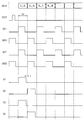
도 3은 도 1에 도시된 게이트 구동부에 대한 블록도이다. 도 4는 도 3의 게이트 구동부에 따른 입출력 신호에 대한 파형도이다.3 is a block diagram of the gate driver shown in FIG. 4 is a waveform diagram of an input / output signal according to the gate driver of FIG.
도 1, 도 3 및 도 4를 참조하면, 상기 게이트 구동부(250)는 복수의 쉬프트 레지스터들(SR1,..., SRn)을 포함하고, 상기 쉬프트 레지스터들(SR1,..., SRn)은 제1 내지 제n 게이트 신호들(G1,..., Gn)을 제1 내지 제n 게이트 라인들(GL1,..., GLn)에 출력한다. 1, 3, and 4, the
상기 게이트 구동부(250)는 상기 제어 회로부(210)로부터 상기 수직 개시 신호(STV), 상기 제1 클럭 신호(CPV1), 상기 제2 클럭 신호(CPV2), 제3 클럭 신호(CPV3), 제4 클럭 신호(CPV4), 게이트 온 신호(VON) 및 게이트 오프 신호(VOFF)를 수신한다. The
상기 게이트 구동부(250)는 상기 수직 개시 신호(STV)에 응답하여 상기 제1 클럭 신호(CPV1), 상기 제2 클럭 신호(CPV2), 제3 클럭 신호(CPV3), 제4 클럭 신호(CPV4), 상기 게이트 온 신호(VON) 및 게이트 오프 신호(VOFF)를 이용하여 상기 제1 내지 제n 게이트 신호들(G1,..., Gn)을 생성한다. The
상기 제1 클럭 신호(CPV1)는 제4N-3 쉬프트 레지스터(SR1, SR5,...)의 메인 클럭 신호로서, 제4N-3 게이트 신호(G1, G5,,..)에 포함된 하이 펄스의 라이징 구간을 제어한다. 상기 제2 클럭 신호(CPV2)는 제4N-2 쉬프트 레지스터(SR2, SR6,...)의 메인 클럭 신호로서, 제4N-2 게이트 신호(G2, G6,,..)에 포함된 하이 펄스의 라이징 구간을 제어한다. 상기 제3 클럭 신호(CPV3)는 제4N-1 쉬프트 레지스터(SR3, SR7,...)의 메인 클럭 신호로서, 제4N-1 게이트 신호(G3, G7,,..)에 포함된 하이 펄스의 라이징 구간을 제어한다. 상기 제4 클럭 신호(CPV4)는 제4N 쉬프트 레지스터(SR4, SR8,...)의 메인 클럭 신호로서, 제4N 게이트 신호(G4, G8,,..)에 포함된 하이 펄스의 라이징 구간을 제어한다. 도시된 바와 같이, 상기 제1 및 제3 클럭 신호들(CPV1, CPV3)은 서로 같은 신호이다. 상기 제2 및 제4 클럭 신호들(CPV2, CPV4)은 서로 같은 신호이고 상기 제1 및 제3 클럭 신호들(CPV1, CPV3)과 다른 신호이다. 도 4에 도시된 바와 같이, 제1 및 제3 클럭 신호들(CPV1, CPV3)과 상기 제2 및 제4 클럭 신호들(CPV2, CPV4)은 2 수평 주기(2H) 만큼 지연차를 갖는다. The first clock signal CPV1 is a main clock signal of the fourth N-3 shift register SR1, SR5, ..., and a high pulse included in the fourth N-3 gate signal G1, G5, And controls the rising period of the vehicle. The second clock signal CPV2 is a main clock signal of the fourth N-2 shift registers SR2, SR6, ... and a high pulse included in the fourth N-2 gate signal G2, G6, And controls the rising period of the vehicle. The third clock signal CPV3 is a main clock signal of the fourth N-1 shift register SR3, SR7, ..., and a high pulse included in the 4N-1 gate signal G3, G7, And controls the rising period of the vehicle. The fourth clock signal CPV4 is the main clock signal of the fourth N shift registers SR4, SR8, ... and the rising period of the high pulse included in the fourth N gate signals G4, G8, . As shown, the first and third clock signals CPV1 and CPV3 are the same signal. The second and fourth clock signals CPV2 and CPV4 are the same signal and are different from the first and third clock signals CPV1 and CPV3. As shown in FIG. 4, the first and third clock signals CPV1 and CPV3 and the second and fourth clock signals CPV2 and CPV4 have a delay difference by two
본 실시예에 따르면, 상기 수직 개시 신호(STV)는 제1, 제2, 제3 및 제4 쉬프트 레지스터들(SR1, SR2, SR3, SR4)에 각각 인가된다. 상기 제1, 제2, 제3 및 제4 쉬프트 레지스터들(SR1, SR2, SR3, SR4)은 상기 제1, 제2, 제3 및 제4 클럭 신호들(CPV1, CPV2, CPV3, CPV4) 각각의 라이징 구간에 동기된 상기 제1, 제2, 제3 및 제4 게이트 신호들(G1, G2, G3, G4)을 생성한다. According to the present embodiment, the vertical start signal STV is applied to the first, second, third and fourth shift registers SR1, SR2, SR3 and SR4, respectively. The first, second, third and fourth shift registers SR1, SR2, SR3 and SR4 are connected to the first, second, third and fourth clock signals CPV1, CPV2, CPV3 and CPV4 respectively Second, third, and fourth gate signals G1, G2, G3, and G4 synchronized with the rising period of the gate signal.
상기 제1 및 제3 쉬프트 레지스터들(SR1, SR3)은 같은 신호인 상기 제1 및 제3 클럭 신호들(CPV1, CPV3)에 의해 라이징 구간이 제어된 하이 펄스를 포함하는 상기 제1 및 제3 게이트 신호들(G1, G3)을 출력한다. 상기 제1 및 제3 게이트 신호들(G1, G3)의 상기 하이 펄스는 2 수평 주기(2H)에 대응하는 폭을 가질 수 있다. 상기 제1 및 제3 게이트 신호들(G1, G3)은 제1 및 제3 게이트 라인들에 각각 인가된다. The first and third shift registers SR1 and SR3 are controlled by the first and third clock signals CPV1 and CPV3, And outputs the gate signals G1 and G3. The high pulse of the first and third gate signals G1 and G3 may have a width corresponding to two horizontal periods (2H). The first and third gate signals G1 and G3 are applied to the first and third gate lines, respectively.
상기 제1 및 제3 게이트 신호들(G1, G3)에 동기되어, 상기 데이터 구동부(230)는 제1 및 제3 화소 행들의 데이터 신호(1L_3L)를 데이터 라인들에 출력한다. 따라서, 상기 제1 및 제3 게이트 신호(G1, G3)의 하이 펄스에 응답하여 상기 제1 및 제3 화소 행들의 데이터 신호(1L_3L)는 상기 제1 및 제3 화소 행들에 충전된다. In synchronization with the first and third gate signals G1 and G3, the
이어, 상기 제2 및 제4 쉬프트 레지스터들(SR2, SR4)은 같은 신호인 상기 제2 및 제4 클럭 신호들(CPV2, CPV4)에 의해 라이징 구간이 제어된 하이 펄스를 포함하는 상기 제2 및 제4 게이트 신호들(G2, G4)을 출력한다. 상기 제2 및 제4 게이트 신호들(G2, G4)은 제2 및 제4 게이트 라인들에 각각 인가된다. The second and fourth shift registers SR2 and SR4 are controlled by the second and fourth clock signals CPV2 and CPV4, which are the same signals, And outputs the fourth gate signals G2 and G4. The second and fourth gate signals G2 and G4 are applied to the second and fourth gate lines, respectively.
상기 제2 및 제4 게이트 신호들(G2, G4)에 동기되어, 상기 데이터 구동부(230)는 제2 및 제4 화소 행들의 데이터 신호(2L_4L)를 데이터 라인들에 출력한다. 따라서, 상기 제2 및 제4 게이트 신호들(G2, G4)의 하이 펄스에 응답하여 상기 제2 및 제4 화소 행들의 데이터 신호(2L_4L)는 상기 제2 및 제4 화소 행들에 충전된다. In synchronization with the second and fourth gate signals G2 and G4, the
이때, 상기 제3 게이트 신호의 폴링 구간과 상기 제2 게이트 신호의 라이징 구간이 중첩하는 경우, 상기 제3 게이트 신호의 폴링 구간에 의해 상기 제2 게이트 신호의 라이징 구간에서 전압 강하되는 킥백 전압이 발생할 수 있다. When the polling interval of the third gate signal and the rising interval of the second gate signal are overlapped, a kickback voltage is generated in which the voltage falls in the rising period of the second gate signal due to the polling interval of the third gate signal .
따라서, 본 실시예에서는 상기 킥백 전압의 발생을 막기 위해서, 상기 제1 및 제3 게이트 신호들(G1, G3)에 포함된 하이 펄스의 폴링 구간과 상기 제2 및 제4 게이트 신호들(G2, G4)에 포함된 하이 펄스의 라이징 구간을 일정 구간(d)만큼 이격시킨다. 각 게이트 신호의 하이 펄스의 폴링 구간은 상기 제어 회로부(210)로부터 제공되는 출력 인에이블 신호를 통해 제어될 수 있다. 상기 일정 간격(d)이 최소 약 1㎲ 내지 2㎲ 로 설정될 경우 상기 킥백 전압의 발생을 막을 수 있다. Therefore, in this embodiment, in order to prevent the generation of the kickback voltage, a polling period of the high pulse included in the first and third gate signals G1 and G3 and a second pulse signal of the second and fourth gate signals G2, The rising period of the high pulse included in the first pulse G4 is separated by a predetermined interval d. The polling interval of the high pulse of each gate signal may be controlled through an output enable signal provided from the
이어, 상기 제5 및 제7 쉬프트 레지스터들(SR5, SR7)은 상기 제1 및 제3 클럭 신호들(CPV1, CPV3)에 의해 라이징 구간이 제어된 제5 및 제7 게이트 신호들(G5, G7)을 출력한다. 상기 제5 쉬프트 레지스터(SR5)는 상기 제1 쉬프트 레지스터(SR1)로부터 캐리 신호를 수신하고, 상기 제7 쉬프트 레지스터(SR7)는 상기 제3 쉬프트 레지스터(SR3)로부터 캐기 신호를 수신한다. The fifth and seventh shift registers SR5 and SR7 receive the fifth and seventh gate signals G5 and G7 controlled by the first and third clock signals CPV1 and CPV3, ). The fifth shift register SR5 receives the carry signal from the first shift register SR1 and the seventh shift register SR7 receives the carry signal from the third shift register SR3.
상기 제5 및 제7 게이트 신호들(G5, G7)에 포함된 하이 펄스의 라이징 구간은 상기 제2 및 제4 게이트 신호들(G2, G4)에 포함된 하이 펄스의 폴링 구간과 일정 간격(d)만큼 이격된다.The rising period of the high pulse included in the fifth and seventh gate signals G5 and G7 is equal to the falling period of the high pulse included in the second and fourth gate signals G2 and G4, ).
상기 제5 및 제7 게이트 신호들(G5, G7)에 동기되어, 상기 데이터 구동부(230)는 제5 및 제7 화소 행들의 데이터 신호(5L_7L)를 데이터 라인들에 출력한다. 따라서, 상기 제5 및 제7 게이트 신호들(G5, G7)의 하이 펄스에 응답하여 상기 제5 및 제7 화소 행들의 데이터 신호(5L_7L)는 상기 제5 및 제7 화소 행들에 충전된다. In synchronization with the fifth and seventh gate signals G5 and G7, the
이와 같은 방식으로, 상기 데이터 구동부(230) 및 상기 게이트 구동부(250) 가 구동됨에 따라서, 상기 표시 패널(100)은 두 개의 홀수 번째 화소 행들 및 두 개의 짝수 번째 화소 행들에 순차적으로 영상을 표시할 수 있다. 본 실시예에 따르면 두 개의 화소 행들을 동시에 구동할 수 있으므로 각 화소의 데이터 충전 시간을 2 수평 주기(2H)로 확장할 수 있다. 이에 따라서, HD 해상도 보다 4배 높은 UD 해상도의 대형 패널에서도 충분한 충전 시간에 의해 화소 충전율을 충분히 확보할 수 있다. In this manner, as the
도 5는 본 발명의 다른 실시예에 따른 게이트 구동부에 대한 블록도이다. 도 6은 도 5의 게이트 구동부에 따른 입출력 신호에 대한 파형도이다. 5 is a block diagram of a gate driver according to another embodiment of the present invention. 6 is a waveform diagram of an input / output signal according to the gate driver of FIG.
도 1, 도 5 및 도 6을 참조하면, 상기 게이트 구동부(250)는 복수의 쉬프트 레지스터들(ISR1,..., ISRn)을 포함하고, 상기 쉬프트 레지스터들(ISR1,..., ISRn)은 제1 내지 제n 게이트 신호들(G1,..., Gn)을 제1 내지 제n 게이트 라인들(GL1,.., GLn)을 출력한다. 1, 5, and 6, the
본 실시예에 따른 상기 쉬프트 레지스터들(ISR1,..., ISRn) 각각은 복수의 스위칭 소자들을 포함하고, 상기 스위칭 소자들은 화소(P)의 스위칭 소자와 동일한 제조 공정을 통해서 상기 표시 패널(100)의 제1 영역(A1)에 집적된다. 상기 표시 패널(100)의 제2 영역(A2)에는 다음 게이트 라인에 인가된 다음 게이트 신호에 응답하여 현재 게이트 라인에 인가된 현재 게이트 신호를 로우 레벨, 예컨대, 전원 오프 전압(VSS)으로 풀 다운(Pull-Down)시키는 풀 다운부가 배치될 수 있다. Each of the shift registers ISR1 to ISRn according to the present embodiment includes a plurality of switching elements and the switching elements are connected to the
상기 게이트 구동부(250)는 상기 제어 회로부(210)로부터 상기 수직 개시 신호(STV), 제1 클럭 신호(CK1), 제1 반전 클럭 신호(CKB1), 제2 클럭 신호(CK2), 제2 반전 클럭 신호(CKB2) 및 전원 오프 전압(VSS)을 수신한다. 상기 제1 및 제2 클럭 신호들(CK1, CK2)은 서로 같은 신호이고, 이에 따라서, 상기 제1 및 제2 반전 클럭 신호들(CKB1, CKB2)은 서로 같은 신호이다. The
상기 게이트 구동부(250)는 상기 수직 개시 신호(STVP)에 응답하여 상기 제1 클럭 신호(CK1), 제1 반전 클럭 신호(CKB1), 제2 클럭 신호(CK2), 제2 반전 클럭 신호(CKB2) 및 전원 오프 전압(VSS)을 이용하여 상기 제1 내지 제n 게이트 신호들(G1,..., Gn)을 생성한다. The
상기 제1 클럭 신호(CK1)는 제4N-3 쉬프트 레지스터(ISR1, ISR5,...)의 메인 클럭 신호로서, 제4N-3 게이트 신호(G1, G5,,..)에 포함된 하이 펄스의 라이징 구간을 제어하고, 상기 제1 반전 클럭 신호(CKB1)는 제4N-3 게이트 신호(G1, G5,,..)의 하이 펄스에 대응하는 구간을 제외한 프레임의 나머지 구간 동안 제4N-3 게이트 신호(G1, G5,,..)를 로우 레벨(예컨대, VSS)로 유지시킨다. The first clock signal CK1 is a main clock signal of the fourth N-3 shift registers ISR1, ISR5, ... and is a high pulse included in the fourth N-3 gate signal G1, G5, And the first inverted clock signal CKB1 controls the rising period of the fourth N-3 gate signal G1, G5, ... during the remainder of the frame excluding the section corresponding to the high pulse of the fourth N- And maintains the gate signals G1, G5, ... at a low level (e.g., VSS).
상기 제1 반전 클럭 신호(CKB1)는 제4N-2 쉬프트 레지스터(ISR2, ISR6,...)의 메인 클럭 신호로서, 제4N-2 게이트 신호(G2, G6,,..)에 포함된 하이 펄스의 라이징 구간을 제어하고, 상기 제1 클럭 신호(CK1)는 제4N-2 게이트 신호(G2, G6,,..)의 하이 펄스에 대응하는 구간을 제외한 프레임의 나머지 구간 동안 제4N-2 게이트 신호(G2, G6,,..)를 로우 레벨(예컨대, VSS)로 유지시킨다.The first inverted clock signal CKB1 is a main clock signal of the fourth N-2 shift register ISR2, ISR6, ... and is a main clock signal of the fourth N-2 gate signal G2, G6, The first clock signal CK1 controls the rising period of the fourth N-2 pulse during the remaining period of the frame excluding the period corresponding to the high pulse of the fourth N-2 gate signal G2, G6, And maintains the gate signals G2, G6, ... at a low level (e.g., VSS).
상기 제2 클럭 신호(CK2)는 제4N-1 쉬프트 레지스터(ISR3, ISR7,...)의 메인 클럭 신호로서, 제4N-1 게이트 신호(G3, G7,,..)에 포함된 하이 펄스의 라이징 구간을 제어하고, 상기 제2 반전 클럭 신호(CKB2)는 제4N-1 게이트 신호(G3, G7,,..)의 하이 펄스에 대응하는 구간을 제외한 프레임의 나머지 구간 동안 제4N-1 게이트 신호(G3, G7,,..)를 로우 레벨(예컨대, VSS)로 유지시킨다.The second clock signal CK2 is a main clock signal of the fourth N-1 shift register ISR3, ISR7, ..., and a high pulse included in the (4N-1) th gate signal G3, G7, And the second inverted clock signal CKB2 controls the rising period of the fourth N-1 gate signal (G3, G7, ...) during the remaining period of the frame excluding the period corresponding to the high pulse of the fourth N- And maintains the gate signals G3, G7, ... at a low level (e.g., VSS).
상기 제2 반전 클럭 신호(CKB2)는 제4N 쉬프트 레지스터(ISR4, ISR8,...)의 메인 클럭 신호로서, 제4N 게이트 신호(G4, G8,,..)에 포함된 하이 펄스의 라이징 구간을 제어하고, 제2 클럭 신호(CK2)는 제4N 게이트 신호(G4, G8,,..)의 하이 펄스에 대응하는 구간을 제외한 프레임의 나머지 구간 동안 제4N 게이트 신호(G4, G8,,..)를 로우 레벨(예컨대, VSS)로 유지시킨다.The second inverted clock signal CKB2 is the main clock signal of the fourth N shift registers ISR4, ISR8, ... and the rising period of the high pulse included in the fourth N gate signals G4, G8, And the second clock signal CK2 controls the fourth N gate signals G4, G8, ... during the remainder of the frame excluding the section corresponding to the high pulse of the fourth N gate signals G4, G8, .... ) To a low level (e.g., VSS).
본 실시예에 따르면, 상기 수직 개시 신호(STVP)는 제1, 제2, 제3 및 제4 쉬프트 레지스터들(ISR1, ISR2, ISR3, ISR4)에 각각 인가된다. 상기 제1, 제2, 제3 및 제4 쉬프트 레지스터들(ISR1, ISR2, ISR3, ISR4)은 상기 클럭 신호들(CK1, CKB1, CK2, CKB2) 각각의 라이징 구간에 동기된 상기 제1, 제2, 제3 및 제4 게이트 신호들(G1, G2, G3, G4)을 생성한다. According to the present embodiment, the vertical start signal STVP is applied to the first, second, third and fourth shift registers ISR1, ISR2, ISR3 and ISR4, respectively. The first, second, third and fourth shift registers ISR1, ISR2, ISR3 and ISR4 are connected to the first, second, third and fourth shift registers synchronized with the rising period of each of the clock signals CK1, CKB1, CK2, 2, and third and fourth gate signals G1, G2, G3, and G4.
상기 제1 및 제3 쉬프트 레지스터들(ISR1, ISR3)은 상기 제1 및 제2 클럭 신호들(CK1, CK2)의 의해 라이징 구간이 제어된 상기 제1 및 제3 게이트 신호들(G1, G3)을 출력한다. 상기 제1 및 제3 게이트 신호들(G1, G3)은 같은 구간의 하이 펄스를 포함하고, 상기 하이 펄스는 2 수평 주기(2H)에 대응하는 폭을 가질 수 있다. 상기 제1 및 제3 게이트 신호들(G1, G3)은 제1 및 제2 게이트 라인들에 각각 인가된다. The first and third shift registers ISR1 and ISR3 are controlled by the first and third gate signals G1 and G3 whose rising periods are controlled by the first and second clock signals CK1 and CK2, . The first and third gate signals G1 and G3 include a high pulse of the same interval and the high pulse may have a width corresponding to two
상기 제1 및 제3 게이트 신호들(G1, G3)에 동기되어, 상기 데이터 구동부(230)는 제1 및 제3 화소 행들의 데이터 신호(1L_3L)를 데이터 라인들에 인가한다. 따라서, 상기 제1 및 제3 게이트 신호의 하이 펄스에 응답하여 상기 제1 및 제3 행 데이터 신호(1L_3L)는 상기 제1 및 제3 화소 행들에 충전된다. In synchronization with the first and third gate signals G1 and G3, the
이어, 상기 제2 및 제4 쉬프트 레지스터들(ISR2, ISR4)은 상기 제1 및 제2 반전 클럭 신호들(CKB1, CKB2)에 의해 라이징 구간이 제어된 제2 및 제4 게이트 신호들(G2, G4)을 출력한다. 상기 제2 및 제4 게이트 신호들(G2, G4)은 실질적으로 같은 구간의 하이 펄스를 포함한다. 상기 제2 및 제4 게이트 신호들(G2, G4)은 제2 및 제4 게이트 라인들에 각각 인가된다. The second and fourth shift registers ISR2 and ISR4 are controlled by the first and second inverted clock signals CKB1 and CKB2 to generate second and fourth gate signals G2, G4. The second and fourth gate signals G2 and G4 include a high pulse of substantially the same interval. The second and fourth gate signals G2 and G4 are applied to the second and fourth gate lines, respectively.
상기 제2 및 제4 게이트 신호들(G2, G4)에 동기되어, 상기 데이터 구동부(230)는 제2 및 제4 화소 행들의 데이터 신호(2L_4L)를 데이터 라인들에 출력한다. 따라서, 상기 제2 및 제4 게이트 신호들(G2, G4)의 하이 펄스에 응답하여 상기 제2 및 제4 화소 행들의 데이터 신호(2L_4L)는 상기 제2 및 제4 화소 행들에 충전된다. In synchronization with the second and fourth gate signals G2 and G4, the
본 실시예에서는 킥백 전압의 발생을 막기 위해서, 상기 제1 및 제3 게이트 신호들(G1, G3)에 포함된 하이 펄스의 폴링 구간과 상기 제2 및 제4 게이트 신호들(G2, G4)에 포함된 하이 펄스의 라이징 구간을 일정 구간(d)만큼 이격시킨다. In this embodiment, in order to prevent the generation of a kickback voltage, a polling period of a high pulse included in the first and third gate signals G1 and G3 and a second pulse signal of the second and fourth gate signals G2 and G4 And separates the rising period of the included high pulse by a predetermined period (d).
이상의 본 발명의 실시예들에 따르면, 2개의 홀수 번째 화소 행들 및 2개의 짝수 번째 화소 행들을 순차적으로 구동함으로써 충전 시간을 약 2 수평 주기만큼 확장시킬 수 있다. 또한, 홀수 번째 화소 행과 짝수 번째 화소 행간의 킥백 전압 편차를 제거하여 표시 품질을 향상시킬 수 있다. 또한, 컬럼 반전 모드로 구동할 수 있으므로 소비 전력을 줄일 수 있다. According to the embodiments of the present invention described above, the charge time can be extended by about two horizontal periods by sequentially driving two odd-numbered pixel rows and two even-numbered pixel rows. In addition, the display quality can be improved by eliminating the kickback voltage deviation between the odd-numbered pixel rows and the even-numbered pixel rows. In addition, since it can be driven in the column inversion mode, power consumption can be reduced.
이상 실시예를 참조하여 설명하였지만, 해당 기술 분야의 숙련된 당업자는 하기의 특허 청구의 범위에 기재된 본 발명의 사상 및 영역으로부터 벗어나지 않는 범위 내에서 본 발명을 다양하게 수정 및 변경시킬 수 있음을 이해할 수 있을 것이다.It will be understood by those skilled in the art that various changes in form and details may be made therein without departing from the spirit and scope of the invention as defined in the appended claims. It will be possible.
100 : 표시 패널 200 : 표시 구동부
210 : 제어 회로부 230 : 데이터 구동부
250 : 게이트 구동부 251, 252 : 제1 및 제2 게이트 회로부100: display panel 200: display driver
210: control circuit unit 230:
250: gate driving units 251 and 252: first and second gate circuit units
Claims (20)
같은 화소 행의 화소들과 연결된 게이트 라인;
같은 화소 열에 포함된 화소들에 연결된 제1 데이터 라인; 및
상기 같은 화소 열의 화소들 중 상기 제1 데이터 라인에 연결된 화소들을 제외한 나머지 화소들에 연결된 제2 데이터 라인을 포함하는 표시 패널.A plurality of pixels arranged in a pixel row and a pixel column;
A gate line connected to pixels of the same pixel row;
A first data line connected to the pixels included in the same pixel column; And
And a second data line connected to the remaining pixels except the pixels connected to the first data line among the pixels of the same pixel column.
상기 제1 화소 열과 인접한 제2 화소 열의 화소들에 연결된 제3 데이터 라인; 및
상기 제2 화소 열의 화소들 중 상기 제3 데이터 라인에 연결된 화소들을 제외한 나머지 화소들에 연결된 제4 데이터 라인을 더 포함하는 표시 패널.3. The method of claim 2, wherein the first and second data lines are coupled to pixels of the first column,
A third data line connected to the pixels of the second pixel column adjacent to the first pixel column; And
And a fourth data line connected to the remaining pixels except the pixels connected to the third data line among the pixels of the second pixel column.
상기 제2 화소 열의 화소들 중 제4N-1 및 제4N 화소들은 상기 제2 데이터 라인과 인접한 제3 데이터 라인에 연결되고, 상기 제2 화소 열의 화소들 중 제4N-3 및 제4N-2 화소들은 상기 제3 데이터 라인과 인접한 제4 데이터 라인에 연결된 것을 특징으로 하는 표시 패널(N은 1,2,3... 인 자연수임). The liquid crystal display of claim 3, wherein the fourth N-3 and fourth N-2 pixels among the pixels of the first pixel column are connected to the first data line, and the fourth N-1 and fourth N pixels Are connected to the second data line adjacent to the first data line,
And fourth N-1 and fourth N pixels among the pixels of the second pixel column are connected to a third data line adjacent to the second data line, and the fourth N-3 and fourth N-2 pixels (N is a natural number of 1, 2, 3,...) Connected to the fourth data line adjacent to the third data line.
2개의 게이트 신호들을 동시에 출력하는 게이트 구동부; 및
2 개의 화소 행들에 대응하는 데이터 신호를 출력하는 데이터 구동부를 포함하는 표시 장치.A display panel including a plurality of pixels arranged in a pixel row and a pixel column, a gate line connected to pixels in the same pixel row, a first data line connected to pixels included in the same pixel column, and a second data line;
A gate driver for simultaneously outputting two gate signals; And
And a data driver for outputting a data signal corresponding to two pixel rows.
상기 제1 화소 열과 인접한 제2 화소 열의 화소들에 연결된 제3 데이터 라인; 및
상기 제2 화소 열의 화소들 중 상기 제3 데이터 라인에 연결된 화소들을 제외한 나머지 화소들에 연결된 제4 데이터 라인을 더 포함하는 표시 장치.11. The display device according to claim 10, wherein the first and second data lines are connected to pixels of a first pixel column,
A third data line connected to the pixels of the second pixel column adjacent to the first pixel column; And
And a fourth data line connected to the remaining pixels except the pixels connected to the third data line among the pixels of the second pixel column.
상기 제2 화소 열의 화소들 중 제4N-1 및 제4N 화소들은 상기 제2 데이터 라인과 인접한 제3 데이터 라인에 연결되고, 상기 제2 화소 열의 화소들 중 제4N-3 및 제4N-2 화소들은 상기 제3 데이터 라인과 인접한 제4 데이터 라인에 연결된 것을 특징으로 하는 표시 패널(N은 1,2,3... 인 자연수임). The liquid crystal display of claim 11, wherein the fourth N-3 and fourth N-2 pixels among the pixels of the first pixel column are connected to the first data line, and the fourth N-1 and fourth N pixels Are connected to the second data line adjacent to the first data line,
And fourth N-1 and fourth N pixels among the pixels of the second pixel column are connected to a third data line adjacent to the second data line, and the fourth N-3 and fourth N-2 pixels (N is a natural number of 1, 2, 3,...) Connected to the fourth data line adjacent to the third data line.
제1 클럭 신호에 기초하여 제4N-3 게이트 신호에 포함된 하이 펄스의 라이징 구간을 제어하고, 제2 클럭 신호에 기초하여 제4N-2 게이트 신호에 포함된 하이 펄스의 라이징 구간을 제어하고, 제3 클럭 신호에 기초하여 제4N-1 게이트 신호에 포함된 하이 펄스의 라이징 구간을 제어하고, 제4 클럭 신호에 기초하여 제4N 게이트 신호에 포함된 하이 펄스의 라이징 구간을 제어하는 것을 특징으로 하는 표시 장치. 16. The method of claim 15, wherein the gate driver
Controls the rising period of the high pulse included in the fourth N-3 gate signal based on the first clock signal, controls the rising period of the high pulse included in the fourth N-2 gate signal based on the second clock signal, Controls the rising period of the high pulse included in the fourth N-1 gate signal based on the third clock signal, and controls the rising period of the high pulse included in the fourth N gate signal based on the fourth clock signal / RTI >
제1 클럭 신호에 기초하여 제4N-3 게이트 신호에 포함된 하이 펄스의 라이징 구간을 제어하고, 상기 제1 클럭 신호에 반전된 제1 반전 클럭 신호에 기초하여 제4N-2 게이트 신호에 포함된 하이 펄스의 라이징 구간을 제어하고, 제2 클럭 신호에 기초하여 제4N-1 게이트 신호에 포함된 하이 펄스의 라이징 구간을 제어하고, 상기 제2 클럭 신호에 반전된 제2 반전 클럭 신호에 기초하여 제4N 게이트 신호에 포함된 하이 펄스의 라이징 구간을 제어하는 것을 특징으로 하는 표시 장치. 19. The method of claim 18, wherein the gate driver
And controls the rising period of the high pulse included in the fourth N-3 gate signal based on the first clock signal, and controls the rising period of the high-pulse included in the fourth N-2 gate signal based on the first inverted clock signal inverted to the first clock signal Controls the rising period of the high pulse and controls the rising period of the high pulse included in the fourth N-1 gate signal based on the second clock signal, and based on the second inverted clock signal inverted to the second clock signal And controls the rising period of the high pulse included in the fourth N gate signal.
Priority Applications (2)
| Application Number | Priority Date | Filing Date | Title |
|---|---|---|---|
| KR1020130078969A KR20150005259A (en) | 2013-07-05 | 2013-07-05 | Display panel and display apparatus having the same |
| US14/310,593 US9472154B2 (en) | 2013-07-05 | 2014-06-20 | Display panel and display apparatus having the same |
Applications Claiming Priority (1)
| Application Number | Priority Date | Filing Date | Title |
|---|---|---|---|
| KR1020130078969A KR20150005259A (en) | 2013-07-05 | 2013-07-05 | Display panel and display apparatus having the same |
Publications (1)
| Publication Number | Publication Date |
|---|---|
| KR20150005259A true KR20150005259A (en) | 2015-01-14 |
Family
ID=52132447
Family Applications (1)
| Application Number | Title | Priority Date | Filing Date |
|---|---|---|---|
| KR1020130078969A Withdrawn KR20150005259A (en) | 2013-07-05 | 2013-07-05 | Display panel and display apparatus having the same |
Country Status (2)
| Country | Link |
|---|---|
| US (1) | US9472154B2 (en) |
| KR (1) | KR20150005259A (en) |
Families Citing this family (9)
| Publication number | Priority date | Publication date | Assignee | Title |
|---|---|---|---|---|
| CN105319794A (en) * | 2015-11-26 | 2016-02-10 | 深圳市华星光电技术有限公司 | Liquid crystal panel, liquid crystal display device and pixel array |
| CN107450225B (en) * | 2017-09-22 | 2020-03-24 | 昆山龙腾光电股份有限公司 | Display panel and display device |
| CN109036281A (en) * | 2018-08-17 | 2018-12-18 | 京东方科技集团股份有限公司 | A kind of driving circuit, display panel and its control method |
| CN109192161A (en) * | 2018-10-08 | 2019-01-11 | 惠科股份有限公司 | Display driving method and device and display device |
| CN109584840B (en) * | 2019-01-30 | 2020-12-29 | 惠科股份有限公司 | Driving method and device of display panel |
| CN111243441B (en) | 2020-03-11 | 2021-12-28 | 京东方科技集团股份有限公司 | Display panel, driving method thereof and display device |
| CN113920956B (en) * | 2020-12-30 | 2024-02-02 | 北京奕斯伟计算技术股份有限公司 | Driving circuit, driving method and display device |
| KR102833886B1 (en) * | 2021-03-15 | 2025-07-16 | 삼성디스플레이 주식회사 | Display device and method of driving display device |
| CN118743328A (en) * | 2023-01-29 | 2024-10-01 | 京东方科技集团股份有限公司 | Display substrate, display panel and display device |
Family Cites Families (15)
| Publication number | Priority date | Publication date | Assignee | Title |
|---|---|---|---|---|
| KR20070034381A (en) | 2005-09-23 | 2007-03-28 | 엘지.필립스 엘시디 주식회사 | LCD and its driving method |
| KR101211237B1 (en) | 2005-12-30 | 2012-12-11 | 엘지디스플레이 주식회사 | Liquid crystal display device and method driving of tha same |
| KR20070109296A (en) | 2006-05-10 | 2007-11-15 | 엘지.필립스 엘시디 주식회사 | LCD and its driving method |
| KR101248900B1 (en) | 2006-05-15 | 2013-04-09 | 엘지디스플레이 주식회사 | A driving method of FSC LCD |
| KR20080105827A (en) | 2007-06-01 | 2008-12-04 | 엘지디스플레이 주식회사 | LCD Display |
| KR20090006997A (en) | 2007-07-13 | 2009-01-16 | 엘지디스플레이 주식회사 | Display |
| KR101435527B1 (en) | 2007-07-25 | 2014-08-29 | 삼성디스플레이 주식회사 | Display device |
| KR101448904B1 (en) | 2007-08-07 | 2014-10-13 | 삼성디스플레이 주식회사 | Display apparatus |
| TWI377551B (en) | 2007-09-26 | 2012-11-21 | Chunghwa Picture Tubes Ltd | Flat panel display |
| KR20090126764A (en) | 2008-06-05 | 2009-12-09 | 삼성전자주식회사 | Display substrate, manufacturing method thereof and display device having same |
| KR101577826B1 (en) | 2009-05-27 | 2015-12-16 | 엘지디스플레이 주식회사 | Image display device and driving method of thereof |
| KR101641958B1 (en) | 2010-03-10 | 2016-07-25 | 삼성디스플레이 주식회사 | Liquid crsytal display |
| KR101710611B1 (en) * | 2010-07-30 | 2017-02-28 | 삼성디스플레이 주식회사 | Method of driving a display panel and display device performing the method |
| KR101832409B1 (en) * | 2011-05-17 | 2018-02-27 | 삼성디스플레이 주식회사 | Gate driver and liquid crystal display including the same |
| KR102029089B1 (en) * | 2012-12-18 | 2019-10-08 | 삼성디스플레이 주식회사 | Display device and driving method thereof |
-
2013
- 2013-07-05 KR KR1020130078969A patent/KR20150005259A/en not_active Withdrawn
-
2014
- 2014-06-20 US US14/310,593 patent/US9472154B2/en active Active
Also Published As
| Publication number | Publication date |
|---|---|
| US9472154B2 (en) | 2016-10-18 |
| US20150009109A1 (en) | 2015-01-08 |
Similar Documents
| Publication | Publication Date | Title |
|---|---|---|
| JP5296829B2 (en) | Liquid crystal display panel and display device having the same | |
| KR100945581B1 (en) | LCD and its driving method | |
| US8400390B2 (en) | Gate driving device and liquid crystal display having the same | |
| KR101692656B1 (en) | Gate driving circuit, display device and driving method | |
| JP4244227B2 (en) | Driving device and driving method for liquid crystal display device | |
| KR101142995B1 (en) | Display device and driving method thereof | |
| KR101211219B1 (en) | Liquid crystal display and driving method thereof | |
| KR20150005259A (en) | Display panel and display apparatus having the same | |
| KR101943000B1 (en) | Liquid crystal display device inculding inspection circuit and inspection method thereof | |
| KR102025858B1 (en) | Display device | |
| CN102110424B (en) | Liquid crystal display device | |
| CN101154006A (en) | LCD Monitor | |
| KR20060023395A (en) | LCD and its driving method | |
| US8624814B2 (en) | Liquid crystal display and inversion driving method thereof | |
| KR102290615B1 (en) | Display Device | |
| KR101147091B1 (en) | Apparatus for driving liquid crystal display device | |
| KR101157941B1 (en) | Apparatus and method for driving liquid crystal display device | |
| KR20060067291A (en) | Display device | |
| CN1967646B (en) | Driving apparatus for liquid crystal display | |
| KR102480834B1 (en) | Display Device Being Capable Of Driving In Low-Speed | |
| KR101157962B1 (en) | Apparatus and method for driving liquid crystal display device | |
| KR20120119019A (en) | Liquid crystal display device | |
| KR20060096859A (en) | LCD and its driving method | |
| KR102082662B1 (en) | Liquid crystal display device | |
| KR20070070639A (en) | Drive of display device |
Legal Events
| Date | Code | Title | Description |
|---|---|---|---|
| PA0109 | Patent application |
Patent event code: PA01091R01D Comment text: Patent Application Patent event date: 20130705 |
|
| PG1501 | Laying open of application | ||
| PC1203 | Withdrawal of no request for examination | ||
| WITN | Application deemed withdrawn, e.g. because no request for examination was filed or no examination fee was paid |