KR102509185B1 - 유기발광다이오드 표시 패널, 이를 구비하는 유기발광다이오드 표시 장치 및 이의 구동 방법 - Google Patents
유기발광다이오드 표시 패널, 이를 구비하는 유기발광다이오드 표시 장치 및 이의 구동 방법 Download PDFInfo
- Publication number
- KR102509185B1 KR102509185B1 KR1020150136459A KR20150136459A KR102509185B1 KR 102509185 B1 KR102509185 B1 KR 102509185B1 KR 1020150136459 A KR1020150136459 A KR 1020150136459A KR 20150136459 A KR20150136459 A KR 20150136459A KR 102509185 B1 KR102509185 B1 KR 102509185B1
- Authority
- KR
- South Korea
- Prior art keywords
- transistor
- signal
- control signal
- light emitting
- emitting diode
- Prior art date
- Legal status (The legal status is an assumption and is not a legal conclusion. Google has not performed a legal analysis and makes no representation as to the accuracy of the status listed.)
- Active
Links
Images


Classifications
-
- G—PHYSICS
- G09—EDUCATION; CRYPTOGRAPHY; DISPLAY; ADVERTISING; SEALS
- G09G—ARRANGEMENTS OR CIRCUITS FOR CONTROL OF INDICATING DEVICES USING STATIC MEANS TO PRESENT VARIABLE INFORMATION
- G09G3/00—Control arrangements or circuits, of interest only in connection with visual indicators other than cathode-ray tubes
- G09G3/20—Control arrangements or circuits, of interest only in connection with visual indicators other than cathode-ray tubes for presentation of an assembly of a number of characters, e.g. a page, by composing the assembly by combination of individual elements arranged in a matrix no fixed position being assigned to or needed to be assigned to the individual characters or partial characters
- G09G3/22—Control arrangements or circuits, of interest only in connection with visual indicators other than cathode-ray tubes for presentation of an assembly of a number of characters, e.g. a page, by composing the assembly by combination of individual elements arranged in a matrix no fixed position being assigned to or needed to be assigned to the individual characters or partial characters using controlled light sources
- G09G3/30—Control arrangements or circuits, of interest only in connection with visual indicators other than cathode-ray tubes for presentation of an assembly of a number of characters, e.g. a page, by composing the assembly by combination of individual elements arranged in a matrix no fixed position being assigned to or needed to be assigned to the individual characters or partial characters using controlled light sources using electroluminescent panels
- G09G3/32—Control arrangements or circuits, of interest only in connection with visual indicators other than cathode-ray tubes for presentation of an assembly of a number of characters, e.g. a page, by composing the assembly by combination of individual elements arranged in a matrix no fixed position being assigned to or needed to be assigned to the individual characters or partial characters using controlled light sources using electroluminescent panels semiconductive, e.g. using light-emitting diodes [LED]
- G09G3/3208—Control arrangements or circuits, of interest only in connection with visual indicators other than cathode-ray tubes for presentation of an assembly of a number of characters, e.g. a page, by composing the assembly by combination of individual elements arranged in a matrix no fixed position being assigned to or needed to be assigned to the individual characters or partial characters using controlled light sources using electroluminescent panels semiconductive, e.g. using light-emitting diodes [LED] organic, e.g. using organic light-emitting diodes [OLED]
- G09G3/3225—Control arrangements or circuits, of interest only in connection with visual indicators other than cathode-ray tubes for presentation of an assembly of a number of characters, e.g. a page, by composing the assembly by combination of individual elements arranged in a matrix no fixed position being assigned to or needed to be assigned to the individual characters or partial characters using controlled light sources using electroluminescent panels semiconductive, e.g. using light-emitting diodes [LED] organic, e.g. using organic light-emitting diodes [OLED] using an active matrix
- G09G3/3233—Control arrangements or circuits, of interest only in connection with visual indicators other than cathode-ray tubes for presentation of an assembly of a number of characters, e.g. a page, by composing the assembly by combination of individual elements arranged in a matrix no fixed position being assigned to or needed to be assigned to the individual characters or partial characters using controlled light sources using electroluminescent panels semiconductive, e.g. using light-emitting diodes [LED] organic, e.g. using organic light-emitting diodes [OLED] using an active matrix with pixel circuitry controlling the current through the light-emitting element
-
- G—PHYSICS
- G09—EDUCATION; CRYPTOGRAPHY; DISPLAY; ADVERTISING; SEALS
- G09G—ARRANGEMENTS OR CIRCUITS FOR CONTROL OF INDICATING DEVICES USING STATIC MEANS TO PRESENT VARIABLE INFORMATION
- G09G3/00—Control arrangements or circuits, of interest only in connection with visual indicators other than cathode-ray tubes
- G09G3/20—Control arrangements or circuits, of interest only in connection with visual indicators other than cathode-ray tubes for presentation of an assembly of a number of characters, e.g. a page, by composing the assembly by combination of individual elements arranged in a matrix no fixed position being assigned to or needed to be assigned to the individual characters or partial characters
- G09G3/22—Control arrangements or circuits, of interest only in connection with visual indicators other than cathode-ray tubes for presentation of an assembly of a number of characters, e.g. a page, by composing the assembly by combination of individual elements arranged in a matrix no fixed position being assigned to or needed to be assigned to the individual characters or partial characters using controlled light sources
- G09G3/30—Control arrangements or circuits, of interest only in connection with visual indicators other than cathode-ray tubes for presentation of an assembly of a number of characters, e.g. a page, by composing the assembly by combination of individual elements arranged in a matrix no fixed position being assigned to or needed to be assigned to the individual characters or partial characters using controlled light sources using electroluminescent panels
- G09G3/32—Control arrangements or circuits, of interest only in connection with visual indicators other than cathode-ray tubes for presentation of an assembly of a number of characters, e.g. a page, by composing the assembly by combination of individual elements arranged in a matrix no fixed position being assigned to or needed to be assigned to the individual characters or partial characters using controlled light sources using electroluminescent panels semiconductive, e.g. using light-emitting diodes [LED]
- G09G3/3208—Control arrangements or circuits, of interest only in connection with visual indicators other than cathode-ray tubes for presentation of an assembly of a number of characters, e.g. a page, by composing the assembly by combination of individual elements arranged in a matrix no fixed position being assigned to or needed to be assigned to the individual characters or partial characters using controlled light sources using electroluminescent panels semiconductive, e.g. using light-emitting diodes [LED] organic, e.g. using organic light-emitting diodes [OLED]
-
- G—PHYSICS
- G09—EDUCATION; CRYPTOGRAPHY; DISPLAY; ADVERTISING; SEALS
- G09G—ARRANGEMENTS OR CIRCUITS FOR CONTROL OF INDICATING DEVICES USING STATIC MEANS TO PRESENT VARIABLE INFORMATION
- G09G2300/00—Aspects of the constitution of display devices
- G09G2300/08—Active matrix structure, i.e. with use of active elements, inclusive of non-linear two terminal elements, in the pixels together with light emitting or modulating elements
- G09G2300/0809—Several active elements per pixel in active matrix panels
- G09G2300/0814—Several active elements per pixel in active matrix panels used for selection purposes, e.g. logical AND for partial update
-
- G—PHYSICS
- G09—EDUCATION; CRYPTOGRAPHY; DISPLAY; ADVERTISING; SEALS
- G09G—ARRANGEMENTS OR CIRCUITS FOR CONTROL OF INDICATING DEVICES USING STATIC MEANS TO PRESENT VARIABLE INFORMATION
- G09G2300/00—Aspects of the constitution of display devices
- G09G2300/08—Active matrix structure, i.e. with use of active elements, inclusive of non-linear two terminal elements, in the pixels together with light emitting or modulating elements
- G09G2300/0809—Several active elements per pixel in active matrix panels
- G09G2300/0819—Several active elements per pixel in active matrix panels used for counteracting undesired variations, e.g. feedback or autozeroing
-
- G—PHYSICS
- G09—EDUCATION; CRYPTOGRAPHY; DISPLAY; ADVERTISING; SEALS
- G09G—ARRANGEMENTS OR CIRCUITS FOR CONTROL OF INDICATING DEVICES USING STATIC MEANS TO PRESENT VARIABLE INFORMATION
- G09G2300/00—Aspects of the constitution of display devices
- G09G2300/08—Active matrix structure, i.e. with use of active elements, inclusive of non-linear two terminal elements, in the pixels together with light emitting or modulating elements
- G09G2300/0809—Several active elements per pixel in active matrix panels
- G09G2300/0842—Several active elements per pixel in active matrix panels forming a memory circuit, e.g. a dynamic memory with one capacitor
- G09G2300/0861—Several active elements per pixel in active matrix panels forming a memory circuit, e.g. a dynamic memory with one capacitor with additional control of the display period without amending the charge stored in a pixel memory, e.g. by means of additional select electrodes
- G09G2300/0866—Several active elements per pixel in active matrix panels forming a memory circuit, e.g. a dynamic memory with one capacitor with additional control of the display period without amending the charge stored in a pixel memory, e.g. by means of additional select electrodes by means of changes in the pixel supply voltage
-
- G—PHYSICS
- G09—EDUCATION; CRYPTOGRAPHY; DISPLAY; ADVERTISING; SEALS
- G09G—ARRANGEMENTS OR CIRCUITS FOR CONTROL OF INDICATING DEVICES USING STATIC MEANS TO PRESENT VARIABLE INFORMATION
- G09G2310/00—Command of the display device
- G09G2310/02—Addressing, scanning or driving the display screen or processing steps related thereto
- G09G2310/0243—Details of the generation of driving signals
- G09G2310/0251—Precharge or discharge of pixel before applying new pixel voltage
-
- G—PHYSICS
- G09—EDUCATION; CRYPTOGRAPHY; DISPLAY; ADVERTISING; SEALS
- G09G—ARRANGEMENTS OR CIRCUITS FOR CONTROL OF INDICATING DEVICES USING STATIC MEANS TO PRESENT VARIABLE INFORMATION
- G09G2310/00—Command of the display device
- G09G2310/02—Addressing, scanning or driving the display screen or processing steps related thereto
- G09G2310/0264—Details of driving circuits
- G09G2310/0286—Details of a shift registers arranged for use in a driving circuit
-
- G—PHYSICS
- G09—EDUCATION; CRYPTOGRAPHY; DISPLAY; ADVERTISING; SEALS
- G09G—ARRANGEMENTS OR CIRCUITS FOR CONTROL OF INDICATING DEVICES USING STATIC MEANS TO PRESENT VARIABLE INFORMATION
- G09G2310/00—Command of the display device
- G09G2310/08—Details of timing specific for flat panels, other than clock recovery
-
- G—PHYSICS
- G09—EDUCATION; CRYPTOGRAPHY; DISPLAY; ADVERTISING; SEALS
- G09G—ARRANGEMENTS OR CIRCUITS FOR CONTROL OF INDICATING DEVICES USING STATIC MEANS TO PRESENT VARIABLE INFORMATION
- G09G2320/00—Control of display operating conditions
- G09G2320/02—Improving the quality of display appearance
- G09G2320/0252—Improving the response speed
-
- G—PHYSICS
- G09—EDUCATION; CRYPTOGRAPHY; DISPLAY; ADVERTISING; SEALS
- G09G—ARRANGEMENTS OR CIRCUITS FOR CONTROL OF INDICATING DEVICES USING STATIC MEANS TO PRESENT VARIABLE INFORMATION
- G09G2320/00—Control of display operating conditions
- G09G2320/02—Improving the quality of display appearance
- G09G2320/0257—Reduction of after-image effects
-
- G—PHYSICS
- G09—EDUCATION; CRYPTOGRAPHY; DISPLAY; ADVERTISING; SEALS
- G09G—ARRANGEMENTS OR CIRCUITS FOR CONTROL OF INDICATING DEVICES USING STATIC MEANS TO PRESENT VARIABLE INFORMATION
- G09G2330/00—Aspects of power supply; Aspects of display protection and defect management
-
- G—PHYSICS
- G09—EDUCATION; CRYPTOGRAPHY; DISPLAY; ADVERTISING; SEALS
- G09G—ARRANGEMENTS OR CIRCUITS FOR CONTROL OF INDICATING DEVICES USING STATIC MEANS TO PRESENT VARIABLE INFORMATION
- G09G2330/00—Aspects of power supply; Aspects of display protection and defect management
- G09G2330/04—Display protection
Landscapes
- Engineering & Computer Science (AREA)
- Physics & Mathematics (AREA)
- Computer Hardware Design (AREA)
- General Physics & Mathematics (AREA)
- Theoretical Computer Science (AREA)
- Control Of El Displays (AREA)
- Control Of Indicators Other Than Cathode Ray Tubes (AREA)
- Electroluminescent Light Sources (AREA)
Abstract
본 발명은 구동 트랜지스터(T_dr)의 전단에 추가로 스위칭 트랜지스터(T5)를 구비함으로써, 화소의 초기화 구간에서 고전위 전압(VDD_EL)과 기준 전압(Vref) 사이의 충돌(Short) 발생을 해결하여, 구동 트랜지스터(T_dr)의 게이트 노드에 인가되는 초기화 전압을 낮출 수 있도록 한다. 이에 따라 본 발명에 따른 유기발광다이오드 표시 장치는, 샘플링에 사용되는 초기 전압값의 편차 감소에 따른 화소의 응답 특성 향상 등과 같은 여러 가지 효과를 제공할 수 있다.
Description
도 2는 도 1의 유기발광다이오드 표시 장치의 구동 타이밍도이다.
도 3은 도 1의 유기발광다이오드 표시 장치의 초기화 시간에 따른 응답 시간 특성을 나타낸 그래프이다.
도 4는 본 발명의 일 실시예에 따른 유기발광다이오드 표시 장치의 구성을 개략적으로 나타낸 설명도이다.
도 5는 본 발명의 일 실시예에 따른 유기발광다이오드 표시 장치의 화소에 대한 등가 회로도이다.
도 6은 도 5의 유기발광다이오드 표시 장치의 구동 타이밍도이다.
도 7은 본 발명의 다른 실시예에 따른 유기발광다이오드 표시 장치의 화소에 대한 등가 회로도이다.
도 8은 도 7의 유기발광다이오드 표시 장치의 구동 타이밍도이다.
도 9는 본 발명의 또 다른 실시예에 따른 유기발광다이오드 표시 장치의 화소에 대한 등가 회로도이다.
도 10은 도 9의 유기발광다이오드 표시 장치의 구동 타이밍도이다.
도 11은 종래 기술 및 본 발명에 따른 유기발광다이오드 표시 장치의 응답 특성을 비교하기 위한 그래프이다.
410: 표시패널
420: 데이터 구동부
430: 게이트 구동부
440: 타이밍 제어부
Claims (19)
- 서로 교차하여 형성되며 스캔 신호 및 데이터 신호를 각각 전송하는 스캔 라인 및 데이터 라인;
상기 스캔 신호에 대응하여 상기 데이터 신호를 출력단에 인가하는 스위칭 트랜지스터;
상기 데이터 신호에 대응하는 전압을 저장하는 커패시터;
상기 커패시터에 저장된 전압에 대응하여 유기발광다이오드에 인가되는 전류를 결정하는 구동 트랜지스터;
발광 제어 라인과 기준 전압 라인 및 상기 커패시터의 일단 사이에 연결되는 제1 트랜지스터;
상기 스캔 라인과 상기 커패시터의 타단 및 제1 노드 사이에 연결되는, 상기 제1 노드에는 상기 구동 트랜지스터가 연결되는, 제2 트랜지스터;
상기 발광 제어 라인과 상기 제1 노드 및 제2 노드 사이에 연결되는, 상기 제2 노드에는 상기 유기발광다이오드가 연결되는, 제3 트랜지스터;
상기 스캔 라인과 상기 기준 전압 라인 및 상기 제2 노드 사이에 연결되는 제4 트랜지스터; 및
제어 라인과 고전위 전압 단자 및 상기 구동 트랜지스터 사이에 연결되는 제5 트랜지스터;를 포함하고,
화소에 기준 전압이 인가되어 초기화되는 초기화 구간에서, 상기 제5 트랜지스터는 상기 제어 라인을 통해 인가되는 제어 신호에 응답하여 상기 고전위 전압 단자로부터의 고전위 전압 신호가 상기 구동 트랜지스터에 인가되는 것을 차단하는 유기발광다이오드 표시 패널.
- 제 1 항에 있어서,
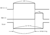
상기 제5 트랜지스터는, 상기 발광 제어 라인을 통해 공급되는 발광 제어 신호(EM(n))의 직전단 신호(EM(n-1))를 상기 제어 신호로 이용하여 상기 고전위 전압 단자의 고전위 전압 신호를 선택적으로 차단하는 유기발광다이오드 표시 패널.
- 제 1 항에 있어서,
상기 제5 트랜지스터는, 상기 발광 제어 라인을 통해 공급되는 발광 제어 신호(EM(n))의 전단 신호(EM(n-k), 단, n>k>1인 자연수)의 가공 신호를 상기 제어 신호로 이용하여 상기 고전위 전압 단자의 고전위 전압 신호를 선택적으로 차단하는 유기발광다이오드 표시 패널.
- 제 1 항에 있어서,
상기 제5 트랜지스터는, 별도의 제어 신호 생성부로부터 생성되어 상기 제어 라인을 통해 공급되는 상기 제어 신호를 이용하여 상기 고전위 전압 단자의 고전위 전압 신호를 선택적으로 차단하는 유기발광다이오드 표시 패널.
- 제 2 항 내지 제 4 항 중 어느 한 항에 있어서,
상기 초기화 구간에서, 상기 제어 신호는, 상기 스캔 신호의 활성화 시점부터 상기 발광 제어 라인을 통해 공급되는 발광 제어 신호(EM(n))의 비활성화 시점까지 상기 제5 트랜지스터를 턴-오프시키는 유기발광다이오드 표시 패널.
- 제 5 항에 있어서,
상기 스캔 신호는, 상기 초기화 구간 및 상기 발광 제어 신호(EM(n))의 비활성화 구간(1H) 동안 상기 스위칭 트랜지스터, 상기 제2 트랜지스터 및 상기 제4 트랜지스터를 턴-오프시키는 유기발광다이오드 표시 패널.
- 영상을 표시하는 표시 패널;
스캔 라인을 통해 상기 표시 패널에 스캔 신호를 공급하는 게이트 구동부;
상기 스캔 신호에 대응되도록, 데이터 라인을 통해 상기 표시 패널에 데이터 신호를 공급하는 데이터 구동부; 및
상기 게이트 구동부 및 상기 데이터 구동부의 구동 타이밍을 제어하는 타이밍 제어부;를 포함하고,
상기 표시 패널은,
상기 스캔 신호에 대응하여 상기 데이터 신호를 출력단에 인가하는 스위칭 트랜지스터;
상기 데이터 신호에 대응하는 전압을 저장하는 커패시터;
상기 커패시터에 저장된 전압에 대응하여 유기발광다이오드에 인가되는 전류를 결정하는 구동 트랜지스터;
발광 제어 라인과 기준 전압 라인 및 상기 커패시터의 일단 사이에 연결되는 제1 트랜지스터;
상기 스캔 라인과 상기 커패시터의 타단 및 제1 노드 사이에 연결되는, 상기 제1 노드에는 상기 구동 트랜지스터가 연결되는, 제2 트랜지스터;
상기 발광 제어 라인과 상기 제1 노드 및 제2 노드 사이에 연결되는, 상기 제2 노드에는 상기 유기발광다이오드가 연결되는, 제3 트랜지스터;
상기 스캔 라인과 상기 기준 전압 라인 및 상기 제2 노드 사이에 연결되는 제4 트랜지스터; 및
제어 라인과 고전위 전압 단자 및 상기 구동 트랜지스터 사이에 연결되는 제5 트랜지스터;를 포함하고,
화소에 기준 전압이 인가되어 초기화되는 초기화 구간에서, 상기 제5 트랜지스터는 상기 제어 라인을 통해 인가되는 제어 신호에 응답하여 상기 고전위 전압 단자로부터의 고전위 전압 신호가 상기 구동 트랜지스터에 인가되는 것을 차단하는 유기발광다이오드 표시 장치.
- 제 7 항에 있어서,
상기 제5 트랜지스터는, 상기 발광 제어 라인을 통해 공급되는 발광 제어 신호(EM(n))의 직전단 신호(EM(n-1))를 상기 제어 신호로 이용하여 상기 고전위 전압 단자의 고전위 전압 신호를 선택적으로 차단하는 유기발광다이오드 표시 장치.
- 제 7 항에 있어서,
상기 제5 트랜지스터는, 상기 발광 제어 라인을 통해 공급되는 발광 제어 신호(EM(n))의 전단 신호(EM(n-k), 단, n>k>1인 자연수)의 가공 신호를 상기 제어 신호로 이용하여 상기 고전위 전압 단자의 고전위 전압 신호를 선택적으로 차단하는 유기발광다이오드 표시 장치.
- 제 7 항에 있어서,
상기 제어 신호를 생성하고, 상기 제어 라인을 통해 상기 제5 트랜지스터에 상기 제어 신호를 공급하는 제어 신호 생성부;를 더 포함하고,
상기 제5 트랜지스터는, 상기 제어 신호 생성부로부터 상기 제어 라인을 통해 공급되는 상기 제어 신호를 이용하여 상기 고전위 전압 단자의 고전위 전압 신호를 선택적으로 차단하는 유기발광다이오드 표시 장치.
- 제 8 항 내지 제 10 항 중 어느 한 항에 있어서,
상기 초기화 구간에서, 상기 제어 신호는, 상기 스캔 신호의 활성화 시점부터 상기 발광 제어 라인을 통해 공급되는 발광 제어 신호(EM(n))의 비활성화 시점까지 상기 제5 트랜지스터를 턴-오프시키는 유기발광다이오드 표시 장치.
- 제 11 항에 있어서,
상기 스캔 신호는, 상기 초기화 구간 및 상기 발광 제어 신호(EM(n))의 비활성화 구간(1H) 동안 상기 스위칭 트랜지스터, 상기 제2 트랜지스터 및 상기 제4 트랜지스터를 턴-오프시키는 유기발광다이오드 표시 장치.
- 서로 교차하여 형성되며 스캔 신호 및 데이터 신호를 각각 전송하는 스캔 라인 및 데이터 라인; 상기 스캔 신호에 대응하여 상기 데이터 신호를 출력단에 인가하는 스위칭 트랜지스터; 상기 데이터 신호에 대응하는 전압을 저장하는 커패시터; 상기 커패시터에 저장된 전압에 대응하여 유기발광다이오드에 인가되는 전류를 결정하는 구동 트랜지스터; 발광 제어 라인과 기준 전압 라인 및 상기 커패시터의 일단 사이에 연결되는 제1 트랜지스터; 상기 스캔 라인과 상기 커패시터의 타단 및 제1 노드 사이에 연결되는, 상기 제1 노드에는 상기 구동 트랜지스터가 연결되는, 제2 트랜지스터; 상기 발광 제어 라인과 상기 제1 노드 및 제2 노드 사이에 연결되는, 상기 제2 노드에는 상기 유기발광다이오드가 연결되는, 제3 트랜지스터; 상기 스캔 라인과 상기 기준 전압 라인 및 상기 제2 노드 사이에 연결되는 제4 트랜지스터; 및 제어 라인과 고전위 전압 단자 및 상기 구동 트랜지스터 사이에 연결되는 제5 트랜지스터;를 포함하는 표시 패널을 구비하는 유기발광다이오드 표시 장치의 구동 방법에 있어서,
(a) 상기 스캔 신호 및 발광 제어 신호(EM(n))가 함께 공급되어 상기 스위칭 트랜지스터, 상기 구동 트랜지스터 및 상기 제1 트랜지스터 내지 상기 제4 트랜지스터를 턴-온(turn on) 시키는 단계;
(b) 상기 발광 제어 신호(EM(n))가 공급되는 동안 제어 신호가 공급되어, 상기 제5 트랜지스터를 턴-오프(turn off)시키는 단계; 및
(c) 상기 스캔 신호 및 상기 발광 제어 신호(EM(n))가 함께 공급되는 동안, 상기 턴 온 된 상기 스위칭 트랜지스터, 상기 구동 트랜지스터 및 상기 제1 트랜지스터 내지 상기 제4 트랜지스터에 기준 전압이 공급되어 초기화가 이루어지는 단계;를 포함하며,
상기 단계 (b)를 통해 턴-오프 된 상기 제5 트랜지스터는, 상기 초기화가 이루어지는 동안 고전위 전압 신호가 상기 구동 트랜지스터로 공급되는 것을 차단하는 유기발광다이오드 표시 장치의 구동 방법.
- 제 13 항에 있어서,
상기 제어 신호는, 상기 발광 제어 신호(EM(n))의 직전단 신호(EM(n-1))로 이루어지는 유기발광다이오드 표시 장치의 구동 방법.
- 제 13 항에 있어서,
상기 제어 신호는, 상기 발광 제어 신호(EM(n))의 전단 신호(EM(n-k), 단, n>k>1인 자연수)의 가공 신호로 이루어지는 유기발광다이오드 표시 장치의 구동 방법.
- 제 13 항에 있어서,
상기 제어 신호는, 별도로 구비되는 제어 신호 생성부에 의해 생성되는 유기발광다이오드 표시 장치의 구동 방법.
- 제 14 항 내지 제 16 항 중 어느 한 항에 있어서,
상기 제어 신호는, 상기 스캔 신호의 활성화 시점부터 상기 발광 제어 신호(EM(n))의 비활성화 시점까지 지속되는 유기발광다이오드 표시 장치의 구동 방법.
- 제 17 항에 있어서,
상기 초기화가 이루어지는 동안 상기 스캔 신호는, 상기 제어 신호의 공급 구간 및 상기 발광 제어 신호(EM(n))의 비활성화 구간(1H) 동안 상기 스위칭 트랜지스터, 상기 제2 트랜지스터 및 상기 제4 트랜지스터를 턴-오프시키는 유기발광다이오드 표시 장치의 구동 방법.
- 서로 교차하여 형성되며 스캔 신호 및 데이터 신호를 각각 전송하는 스캔 라인 및 데이터 라인;
상기 스캔 신호에 대응하여 상기 데이터 신호를 출력단에 인가하는 스위칭 트랜지스터;
상기 데이터 신호에 대응하는 전압을 저장하는 커패시터;
상기 커패시터에 저장된 전압에 대응하여 유기발광다이오드에 인가되는 전류를 결정하는 구동 트랜지스터;
발광 제어 라인과 기준 전압 라인 및 상기 커패시터의 일단 사이에 연결되는 제1 트랜지스터;
상기 스캔 라인과 상기 커패시터의 타단 및 제1 노드 사이에 연결되는, 상기 제1 노드에는 상기 구동 트랜지스터가 연결되는, 제2 트랜지스터;
상기 발광 제어 라인과 상기 제1 노드 및 제2 노드 사이에 연결되는, 상기 제2 노드에는 상기 유기발광다이오드가 연결되는, 제3 트랜지스터;
상기 스캔 라인과 상기 기준 전압 라인 및 상기 제2 노드 사이에 연결되는 제4 트랜지스터; 및
제어 라인과 고전위 전압 단자 및 상기 구동 트랜지스터 사이에 연결되는 제5 트랜지스터;를 포함하고,
상기 제5 트랜지스터는, 화소에 기준 전압이 인가되어 초기화되는 초기화 구간에서, 상기 발광 제어 라인을 통해 공급되는 발광 제어 신호(EM(n))의 직전단 신호(EM(n-1)), 상기 발광 제어 라인을 통해 공급되는 발광 제어 신호(EM(n))의 전단 신호(EM(n-k), 단, n>k>1인 자연수)의 가공 신호, 또는 별도의 제어 신호 생성부로부터 생성되어 상기 제어 라인을 통해 공급되는 신호를 제어 신호로서 이용하여 상기 고전위 전압 단자의 고전위 전압 신호가 상기 구동 트랜지스터에 인가되는 것을 차단하는 유기발광다이오드 표시 패널.
Priority Applications (4)
| Application Number | Priority Date | Filing Date | Title |
|---|---|---|---|
| KR1020150136459A KR102509185B1 (ko) | 2015-09-25 | 2015-09-25 | 유기발광다이오드 표시 패널, 이를 구비하는 유기발광다이오드 표시 장치 및 이의 구동 방법 |
| US15/272,350 US10083656B2 (en) | 2015-09-25 | 2016-09-21 | Organic light-emitting diode (OLED) display panel, OLED display device and method for driving the same |
| CN201610849475.7A CN106847169B (zh) | 2015-09-25 | 2016-09-23 | 有机发光二极管显示面板、有机发光二极管显示装置及其驱动方法 |
| EP16190336.4A EP3147894B1 (en) | 2015-09-25 | 2016-09-23 | Organic light-emitting diode (oled) display panel, oled display device and method for driving the same |
Applications Claiming Priority (1)
| Application Number | Priority Date | Filing Date | Title |
|---|---|---|---|
| KR1020150136459A KR102509185B1 (ko) | 2015-09-25 | 2015-09-25 | 유기발광다이오드 표시 패널, 이를 구비하는 유기발광다이오드 표시 장치 및 이의 구동 방법 |
Publications (2)
| Publication Number | Publication Date |
|---|---|
| KR20170037729A KR20170037729A (ko) | 2017-04-05 |
| KR102509185B1 true KR102509185B1 (ko) | 2023-03-13 |
Family
ID=56990332
Family Applications (1)
| Application Number | Title | Priority Date | Filing Date |
|---|---|---|---|
| KR1020150136459A Active KR102509185B1 (ko) | 2015-09-25 | 2015-09-25 | 유기발광다이오드 표시 패널, 이를 구비하는 유기발광다이오드 표시 장치 및 이의 구동 방법 |
Country Status (4)
| Country | Link |
|---|---|
| US (1) | US10083656B2 (ko) |
| EP (1) | EP3147894B1 (ko) |
| KR (1) | KR102509185B1 (ko) |
| CN (1) | CN106847169B (ko) |
Families Citing this family (19)
| Publication number | Priority date | Publication date | Assignee | Title |
|---|---|---|---|---|
| TWI596592B (zh) * | 2016-10-19 | 2017-08-21 | 創王光電股份有限公司 | 像素補償電路 |
| KR102478679B1 (ko) * | 2017-07-31 | 2022-12-16 | 엘지디스플레이 주식회사 | 전계발광 표시장치 |
| JP7092279B2 (ja) * | 2017-08-16 | 2022-06-28 | 京東方科技集團股▲ふん▼有限公司 | アレイ基板行駆動回路 |
| CN107452331B (zh) * | 2017-08-25 | 2023-12-05 | 京东方科技集团股份有限公司 | 一种像素电路及其驱动方法、显示装置 |
| KR102623352B1 (ko) * | 2017-09-28 | 2024-01-09 | 엘지디스플레이 주식회사 | 유기발광표시장치 및 그의 구동방법 |
| US10423286B1 (en) * | 2018-03-09 | 2019-09-24 | Int Tech Co., Ltd. | Circuit for fingerprint sensing and electronic device comprising the circuit |
| TWI669697B (zh) | 2018-04-19 | 2019-08-21 | 友達光電股份有限公司 | 畫素電路 |
| CN109117733B (zh) * | 2018-07-17 | 2020-06-30 | 武汉华星光电半导体显示技术有限公司 | 一种指纹识别oled显示面板及显示装置 |
| JP7154122B2 (ja) * | 2018-12-20 | 2022-10-17 | エルジー ディスプレイ カンパニー リミテッド | 発光表示装置 |
| KR102622421B1 (ko) | 2018-12-31 | 2024-01-05 | 엘지디스플레이 주식회사 | 발광 다이오드 디스플레이 장치 및 이를 이용한 멀티 스크린 디스플레이 장치 |
| KR102639309B1 (ko) | 2019-06-12 | 2024-02-23 | 삼성디스플레이 주식회사 | 표시 장치 |
| US20210193049A1 (en) * | 2019-12-23 | 2021-06-24 | Apple Inc. | Electronic Display with In-Pixel Compensation and Oxide Drive Transistors |
| CN111341257B (zh) * | 2020-03-24 | 2021-06-15 | 武汉天马微电子有限公司 | 显示面板及其驱动方法、显示装置 |
| KR102791842B1 (ko) * | 2020-07-23 | 2025-04-09 | 삼성디스플레이 주식회사 | 화소 및 이를 포함하는 표시 장치 |
| US11568823B2 (en) * | 2020-08-11 | 2023-01-31 | Everdisplay Optronics (Shanghai) Co., Ltd | Driving method of display panel and display device |
| KR102739031B1 (ko) * | 2021-07-08 | 2024-12-06 | 엘지디스플레이 주식회사 | 픽셀 회로와 이를 포함한 표시장치 |
| EP4300474A4 (en) | 2021-07-30 | 2024-02-28 | BOE Technology Group Co., Ltd. | PIXEL CIRCUIT, CONTROL METHOD AND DISPLAY DEVICE |
| CN115705823B (zh) | 2021-08-05 | 2025-09-16 | 京东方科技集团股份有限公司 | 像素驱动电路及其驱动方法、显示基板和显示装置 |
| KR102740676B1 (ko) * | 2021-09-30 | 2024-12-11 | 엘지디스플레이 주식회사 | 픽셀 회로와 이를 포함한 표시장치 |
Citations (1)
| Publication number | Priority date | Publication date | Assignee | Title |
|---|---|---|---|---|
| US20140152719A1 (en) | 2012-12-04 | 2014-06-05 | Lg Display Co., Ltd. | Pixel circuit, driving method thereof, and organic light emitting display device using the same |
Family Cites Families (3)
| Publication number | Priority date | Publication date | Assignee | Title |
|---|---|---|---|---|
| KR101058115B1 (ko) * | 2009-11-16 | 2011-08-24 | 삼성모바일디스플레이주식회사 | 화소 회로, 유기 전계 발광 표시 장치 |
| KR101920492B1 (ko) * | 2011-09-20 | 2018-11-22 | 엘지디스플레이 주식회사 | 유기발광다이오드 표시장치 |
| KR101517035B1 (ko) * | 2011-12-05 | 2015-05-06 | 엘지디스플레이 주식회사 | 유기발광 다이오드 표시장치 및 그 구동방법 |
-
2015
- 2015-09-25 KR KR1020150136459A patent/KR102509185B1/ko active Active
-
2016
- 2016-09-21 US US15/272,350 patent/US10083656B2/en active Active
- 2016-09-23 EP EP16190336.4A patent/EP3147894B1/en active Active
- 2016-09-23 CN CN201610849475.7A patent/CN106847169B/zh active Active
Patent Citations (1)
| Publication number | Priority date | Publication date | Assignee | Title |
|---|---|---|---|---|
| US20140152719A1 (en) | 2012-12-04 | 2014-06-05 | Lg Display Co., Ltd. | Pixel circuit, driving method thereof, and organic light emitting display device using the same |
Also Published As
| Publication number | Publication date |
|---|---|
| KR20170037729A (ko) | 2017-04-05 |
| EP3147894A1 (en) | 2017-03-29 |
| US10083656B2 (en) | 2018-09-25 |
| CN106847169B (zh) | 2019-06-18 |
| US20170092193A1 (en) | 2017-03-30 |
| CN106847169A (zh) | 2017-06-13 |
| EP3147894B1 (en) | 2019-02-20 |
Similar Documents
| Publication | Publication Date | Title |
|---|---|---|
| KR102509185B1 (ko) | 유기발광다이오드 표시 패널, 이를 구비하는 유기발광다이오드 표시 장치 및 이의 구동 방법 | |
| KR102559087B1 (ko) | 유기 발광 다이오드 디스플레이 장치 | |
| KR102333868B1 (ko) | Oled 표시 장치 | |
| US9842538B2 (en) | Organic light emitting display device and method for driving the same | |
| JP5611312B2 (ja) | 有機発光ダイオード表示装置及びその駆動方法 | |
| US9672769B2 (en) | Display apparatus and method of driving the same | |
| KR20210083644A (ko) | 유기발광 표시장치 및 그 구동방법 | |
| US9196197B2 (en) | Display device and method for driving the same | |
| KR20130123218A (ko) | 유기전계 발광소자 표시장치, 이의 구동회로 및 방법 | |
| KR20170026971A (ko) | 유기 발광 표시장치와 그 구동 장치 및 방법 | |
| KR102569729B1 (ko) | 표시 장치 및 표시 장치의 제어 방법 | |
| KR20160055432A (ko) | 유기발광다이오드 표시장치 | |
| KR102366197B1 (ko) | 표시장치 및 그 구동 방법 | |
| CN109727577B (zh) | 有机发光显示装置及其驱动方法 | |
| CN111883035B (zh) | 显示设备及其驱动方法 | |
| KR102234096B1 (ko) | 스캔 구동부와 이를 포함한 표시장치 | |
| KR102182382B1 (ko) | 유기발광소자표시장치 및 그 구동방법 | |
| JP2023016684A (ja) | 発光素子を制御する画素回路 | |
| US20150124005A1 (en) | Organic light emitting display device and method for driving the same | |
| KR101929037B1 (ko) | 유기발광다이오드 표시장치 | |
| JP6539637B2 (ja) | 有機発光ディスプレイ装置のエミッション信号制御回路及びエミッション信号制御方法、並びに有機発光ディスプレイ装置 | |
| KR20150053475A (ko) | 유기발광다이오드 표시장치의 구동방법 | |
| US10482814B2 (en) | Display device and method for driving same | |
| KR102120344B1 (ko) | 표시장치 및 그의 구동방법 | |
| US12106725B2 (en) | Control device, display apparatus, and control method |
Legal Events
| Date | Code | Title | Description |
|---|---|---|---|
| PA0109 | Patent application |
St.27 status event code: A-0-1-A10-A12-nap-PA0109 |
|
| PG1501 | Laying open of application |
St.27 status event code: A-1-1-Q10-Q12-nap-PG1501 |
|
| P22-X000 | Classification modified |
St.27 status event code: A-2-2-P10-P22-nap-X000 |
|
| A201 | Request for examination | ||
| PA0201 | Request for examination |
St.27 status event code: A-1-2-D10-D11-exm-PA0201 |
|
| E902 | Notification of reason for refusal | ||
| PE0902 | Notice of grounds for rejection |
St.27 status event code: A-1-2-D10-D21-exm-PE0902 |
|
| P11-X000 | Amendment of application requested |
St.27 status event code: A-2-2-P10-P11-nap-X000 |
|
| P13-X000 | Application amended |
St.27 status event code: A-2-2-P10-P13-nap-X000 |
|
| E701 | Decision to grant or registration of patent right | ||
| PE0701 | Decision of registration |
St.27 status event code: A-1-2-D10-D22-exm-PE0701 |
|
| GRNT | Written decision to grant | ||
| PR0701 | Registration of establishment |
St.27 status event code: A-2-4-F10-F11-exm-PR0701 |
|
| PR1002 | Payment of registration fee |
St.27 status event code: A-2-2-U10-U11-oth-PR1002 Fee payment year number: 1 |
|
| PG1601 | Publication of registration |
St.27 status event code: A-4-4-Q10-Q13-nap-PG1601 |
|
| PR1001 | Payment of annual fee |
St.27 status event code: A-4-4-U10-U11-oth-PR1001 Fee payment year number: 4 |
|
| U11 | Full renewal or maintenance fee paid |
Free format text: ST27 STATUS EVENT CODE: A-4-4-U10-U11-OTH-PR1001 (AS PROVIDED BY THE NATIONAL OFFICE) Year of fee payment: 4 |