KR102422074B1 - 표시장치 - Google Patents
표시장치 Download PDFInfo
- Publication number
- KR102422074B1 KR102422074B1 KR1020170103237A KR20170103237A KR102422074B1 KR 102422074 B1 KR102422074 B1 KR 102422074B1 KR 1020170103237 A KR1020170103237 A KR 1020170103237A KR 20170103237 A KR20170103237 A KR 20170103237A KR 102422074 B1 KR102422074 B1 KR 102422074B1
- Authority
- KR
- South Korea
- Prior art keywords
- sensor
- area
- sensor unit
- unit
- layer
- Prior art date
- Legal status (The legal status is an assumption and is not a legal conclusion. Google has not performed a legal analysis and makes no representation as to the accuracy of the status listed.)
- Active
Links
Images


Classifications
-
- G—PHYSICS
- G06—COMPUTING OR CALCULATING; COUNTING
- G06F—ELECTRIC DIGITAL DATA PROCESSING
- G06F3/00—Input arrangements for transferring data to be processed into a form capable of being handled by the computer; Output arrangements for transferring data from processing unit to output unit, e.g. interface arrangements
- G06F3/01—Input arrangements or combined input and output arrangements for interaction between user and computer
- G06F3/03—Arrangements for converting the position or the displacement of a member into a coded form
- G06F3/041—Digitisers, e.g. for touch screens or touch pads, characterised by the transducing means
- G06F3/044—Digitisers, e.g. for touch screens or touch pads, characterised by the transducing means by capacitive means
- G06F3/0446—Digitisers, e.g. for touch screens or touch pads, characterised by the transducing means by capacitive means using a grid-like structure of electrodes in at least two directions, e.g. using row and column electrodes
-
- H01L27/323—
-
- G—PHYSICS
- G06—COMPUTING OR CALCULATING; COUNTING
- G06F—ELECTRIC DIGITAL DATA PROCESSING
- G06F3/00—Input arrangements for transferring data to be processed into a form capable of being handled by the computer; Output arrangements for transferring data from processing unit to output unit, e.g. interface arrangements
- G06F3/01—Input arrangements or combined input and output arrangements for interaction between user and computer
- G06F3/03—Arrangements for converting the position or the displacement of a member into a coded form
- G06F3/041—Digitisers, e.g. for touch screens or touch pads, characterised by the transducing means
- G06F3/0416—Control or interface arrangements specially adapted for digitisers
- G06F3/04164—Connections between sensors and controllers, e.g. routing lines between electrodes and connection pads
-
- G—PHYSICS
- G06—COMPUTING OR CALCULATING; COUNTING
- G06F—ELECTRIC DIGITAL DATA PROCESSING
- G06F3/00—Input arrangements for transferring data to be processed into a form capable of being handled by the computer; Output arrangements for transferring data from processing unit to output unit, e.g. interface arrangements
- G06F3/01—Input arrangements or combined input and output arrangements for interaction between user and computer
- G06F3/03—Arrangements for converting the position or the displacement of a member into a coded form
- G06F3/041—Digitisers, e.g. for touch screens or touch pads, characterised by the transducing means
- G06F3/042—Digitisers, e.g. for touch screens or touch pads, characterised by the transducing means by opto-electronic means
-
- G—PHYSICS
- G06—COMPUTING OR CALCULATING; COUNTING
- G06F—ELECTRIC DIGITAL DATA PROCESSING
- G06F3/00—Input arrangements for transferring data to be processed into a form capable of being handled by the computer; Output arrangements for transferring data from processing unit to output unit, e.g. interface arrangements
- G06F3/01—Input arrangements or combined input and output arrangements for interaction between user and computer
- G06F3/03—Arrangements for converting the position or the displacement of a member into a coded form
- G06F3/041—Digitisers, e.g. for touch screens or touch pads, characterised by the transducing means
- G06F3/044—Digitisers, e.g. for touch screens or touch pads, characterised by the transducing means by capacitive means
- G06F3/0443—Digitisers, e.g. for touch screens or touch pads, characterised by the transducing means by capacitive means using a single layer of sensing electrodes
-
- G—PHYSICS
- G06—COMPUTING OR CALCULATING; COUNTING
- G06F—ELECTRIC DIGITAL DATA PROCESSING
- G06F3/00—Input arrangements for transferring data to be processed into a form capable of being handled by the computer; Output arrangements for transferring data from processing unit to output unit, e.g. interface arrangements
- G06F3/01—Input arrangements or combined input and output arrangements for interaction between user and computer
- G06F3/03—Arrangements for converting the position or the displacement of a member into a coded form
- G06F3/041—Digitisers, e.g. for touch screens or touch pads, characterised by the transducing means
- G06F3/044—Digitisers, e.g. for touch screens or touch pads, characterised by the transducing means by capacitive means
- G06F3/0447—Position sensing using the local deformation of sensor cells
-
- G—PHYSICS
- G06—COMPUTING OR CALCULATING; COUNTING
- G06F—ELECTRIC DIGITAL DATA PROCESSING
- G06F3/00—Input arrangements for transferring data to be processed into a form capable of being handled by the computer; Output arrangements for transferring data from processing unit to output unit, e.g. interface arrangements
- G06F3/01—Input arrangements or combined input and output arrangements for interaction between user and computer
- G06F3/03—Arrangements for converting the position or the displacement of a member into a coded form
- G06F3/041—Digitisers, e.g. for touch screens or touch pads, characterised by the transducing means
- G06F3/044—Digitisers, e.g. for touch screens or touch pads, characterised by the transducing means by capacitive means
- G06F3/0448—Details of the electrode shape, e.g. for enhancing the detection of touches, for generating specific electric field shapes, for enhancing display quality
-
- H01L27/3276—
-
- H01L51/0097—
-
- H01L51/5203—
-
- H—ELECTRICITY
- H10—SEMICONDUCTOR DEVICES; ELECTRIC SOLID-STATE DEVICES NOT OTHERWISE PROVIDED FOR
- H10K—ORGANIC ELECTRIC SOLID-STATE DEVICES
- H10K50/00—Organic light-emitting devices
- H10K50/80—Constructional details
- H10K50/84—Passivation; Containers; Encapsulations
- H10K50/844—Encapsulations
- H10K50/8445—Encapsulations multilayered coatings having a repetitive structure, e.g. having multiple organic-inorganic bilayers
-
- H—ELECTRICITY
- H10—SEMICONDUCTOR DEVICES; ELECTRIC SOLID-STATE DEVICES NOT OTHERWISE PROVIDED FOR
- H10K—ORGANIC ELECTRIC SOLID-STATE DEVICES
- H10K50/00—Organic light-emitting devices
- H10K50/80—Constructional details
- H10K50/86—Arrangements for improving contrast, e.g. preventing reflection of ambient light
-
- H—ELECTRICITY
- H10—SEMICONDUCTOR DEVICES; ELECTRIC SOLID-STATE DEVICES NOT OTHERWISE PROVIDED FOR
- H10K—ORGANIC ELECTRIC SOLID-STATE DEVICES
- H10K59/00—Integrated devices, or assemblies of multiple devices, comprising at least one organic light-emitting element covered by group H10K50/00
- H10K59/10—OLED displays
- H10K59/12—Active-matrix OLED [AMOLED] displays
- H10K59/121—Active-matrix OLED [AMOLED] displays characterised by the geometry or disposition of pixel elements
- H10K59/1213—Active-matrix OLED [AMOLED] displays characterised by the geometry or disposition of pixel elements the pixel elements being TFTs
-
- H—ELECTRICITY
- H10—SEMICONDUCTOR DEVICES; ELECTRIC SOLID-STATE DEVICES NOT OTHERWISE PROVIDED FOR
- H10K—ORGANIC ELECTRIC SOLID-STATE DEVICES
- H10K59/00—Integrated devices, or assemblies of multiple devices, comprising at least one organic light-emitting element covered by group H10K50/00
- H10K59/10—OLED displays
- H10K59/12—Active-matrix OLED [AMOLED] displays
- H10K59/131—Interconnections, e.g. wiring lines or terminals
-
- H—ELECTRICITY
- H10—SEMICONDUCTOR DEVICES; ELECTRIC SOLID-STATE DEVICES NOT OTHERWISE PROVIDED FOR
- H10K—ORGANIC ELECTRIC SOLID-STATE DEVICES
- H10K59/00—Integrated devices, or assemblies of multiple devices, comprising at least one organic light-emitting element covered by group H10K50/00
- H10K59/40—OLEDs integrated with touch screens
-
- H—ELECTRICITY
- H10—SEMICONDUCTOR DEVICES; ELECTRIC SOLID-STATE DEVICES NOT OTHERWISE PROVIDED FOR
- H10K—ORGANIC ELECTRIC SOLID-STATE DEVICES
- H10K59/00—Integrated devices, or assemblies of multiple devices, comprising at least one organic light-emitting element covered by group H10K50/00
- H10K59/80—Constructional details
- H10K59/805—Electrodes
-
- H—ELECTRICITY
- H10—SEMICONDUCTOR DEVICES; ELECTRIC SOLID-STATE DEVICES NOT OTHERWISE PROVIDED FOR
- H10K—ORGANIC ELECTRIC SOLID-STATE DEVICES
- H10K59/00—Integrated devices, or assemblies of multiple devices, comprising at least one organic light-emitting element covered by group H10K50/00
- H10K59/80—Constructional details
- H10K59/88—Dummy elements, i.e. elements having non-functional features
-
- H—ELECTRICITY
- H10—SEMICONDUCTOR DEVICES; ELECTRIC SOLID-STATE DEVICES NOT OTHERWISE PROVIDED FOR
- H10K—ORGANIC ELECTRIC SOLID-STATE DEVICES
- H10K77/00—Constructional details of devices covered by this subclass and not covered by groups H10K10/80, H10K30/80, H10K50/80 or H10K59/80
- H10K77/10—Substrates, e.g. flexible substrates
- H10K77/111—Flexible substrates
-
- G—PHYSICS
- G06—COMPUTING OR CALCULATING; COUNTING
- G06F—ELECTRIC DIGITAL DATA PROCESSING
- G06F2203/00—Indexing scheme relating to G06F3/00 - G06F3/048
- G06F2203/041—Indexing scheme relating to G06F3/041 - G06F3/045
- G06F2203/04102—Flexible digitiser, i.e. constructional details for allowing the whole digitising part of a device to be flexed or rolled like a sheet of paper
-
- G—PHYSICS
- G06—COMPUTING OR CALCULATING; COUNTING
- G06F—ELECTRIC DIGITAL DATA PROCESSING
- G06F2203/00—Indexing scheme relating to G06F3/00 - G06F3/048
- G06F2203/041—Indexing scheme relating to G06F3/041 - G06F3/045
- G06F2203/04103—Manufacturing, i.e. details related to manufacturing processes specially suited for touch sensitive devices
-
- G—PHYSICS
- G06—COMPUTING OR CALCULATING; COUNTING
- G06F—ELECTRIC DIGITAL DATA PROCESSING
- G06F2203/00—Indexing scheme relating to G06F3/00 - G06F3/048
- G06F2203/041—Indexing scheme relating to G06F3/041 - G06F3/045
- G06F2203/04107—Shielding in digitiser, i.e. guard or shielding arrangements, mostly for capacitive touchscreens, e.g. driven shields, driven grounds
-
- G—PHYSICS
- G06—COMPUTING OR CALCULATING; COUNTING
- G06F—ELECTRIC DIGITAL DATA PROCESSING
- G06F2203/00—Indexing scheme relating to G06F3/00 - G06F3/048
- G06F2203/041—Indexing scheme relating to G06F3/041 - G06F3/045
- G06F2203/04111—Cross over in capacitive digitiser, i.e. details of structures for connecting electrodes of the sensing pattern where the connections cross each other, e.g. bridge structures comprising an insulating layer, or vias through substrate
-
- G—PHYSICS
- G06—COMPUTING OR CALCULATING; COUNTING
- G06F—ELECTRIC DIGITAL DATA PROCESSING
- G06F3/00—Input arrangements for transferring data to be processed into a form capable of being handled by the computer; Output arrangements for transferring data from processing unit to output unit, e.g. interface arrangements
- G06F3/01—Input arrangements or combined input and output arrangements for interaction between user and computer
- G06F3/03—Arrangements for converting the position or the displacement of a member into a coded form
- G06F3/041—Digitisers, e.g. for touch screens or touch pads, characterised by the transducing means
- G06F3/0412—Digitisers structurally integrated in a display
-
- H—ELECTRICITY
- H10—SEMICONDUCTOR DEVICES; ELECTRIC SOLID-STATE DEVICES NOT OTHERWISE PROVIDED FOR
- H10K—ORGANIC ELECTRIC SOLID-STATE DEVICES
- H10K59/00—Integrated devices, or assemblies of multiple devices, comprising at least one organic light-emitting element covered by group H10K50/00
- H10K59/80—Constructional details
- H10K59/87—Passivation; Containers; Encapsulations
- H10K59/873—Encapsulations
- H10K59/8731—Encapsulations multilayered coatings having a repetitive structure, e.g. having multiple organic-inorganic bilayers
-
- H—ELECTRICITY
- H10—SEMICONDUCTOR DEVICES; ELECTRIC SOLID-STATE DEVICES NOT OTHERWISE PROVIDED FOR
- H10K—ORGANIC ELECTRIC SOLID-STATE DEVICES
- H10K59/00—Integrated devices, or assemblies of multiple devices, comprising at least one organic light-emitting element covered by group H10K50/00
- H10K59/80—Constructional details
- H10K59/8791—Arrangements for improving contrast, e.g. preventing reflection of ambient light
-
- Y—GENERAL TAGGING OF NEW TECHNOLOGICAL DEVELOPMENTS; GENERAL TAGGING OF CROSS-SECTIONAL TECHNOLOGIES SPANNING OVER SEVERAL SECTIONS OF THE IPC; TECHNICAL SUBJECTS COVERED BY FORMER USPC CROSS-REFERENCE ART COLLECTIONS [XRACs] AND DIGESTS
- Y02—TECHNOLOGIES OR APPLICATIONS FOR MITIGATION OR ADAPTATION AGAINST CLIMATE CHANGE
- Y02E—REDUCTION OF GREENHOUSE GAS [GHG] EMISSIONS, RELATED TO ENERGY GENERATION, TRANSMISSION OR DISTRIBUTION
- Y02E10/00—Energy generation through renewable energy sources
- Y02E10/50—Photovoltaic [PV] energy
- Y02E10/549—Organic PV cells
Landscapes
- Engineering & Computer Science (AREA)
- General Engineering & Computer Science (AREA)
- Theoretical Computer Science (AREA)
- Physics & Mathematics (AREA)
- Human Computer Interaction (AREA)
- General Physics & Mathematics (AREA)
- Microelectronics & Electronic Packaging (AREA)
- Optics & Photonics (AREA)
- Quality & Reliability (AREA)
- Computer Networks & Wireless Communication (AREA)
- Chemical & Material Sciences (AREA)
- Inorganic Chemistry (AREA)
- Geometry (AREA)
- Devices For Indicating Variable Information By Combining Individual Elements (AREA)
- Electroluminescent Light Sources (AREA)
Abstract
Description
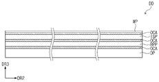
도 2a 내지 2f는 본 발명의 일 실시예에 따른 표시장치의 단면도이다.
도 3은 본 발명의 일 실시예에 따른 표시모듈의 단면도이다.
도 4a 및 도 4b는 본 발명의 일 실시예에 따른 표시패널의 평면도이다.
도 5는 본 발명의 일 실시예에 따른 화소의 등가회로도이다.
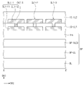
도 6은 본 발명의 일 실시예에 따른 표시패널의 확대된 단면도이다.
도 7a 내지 7d는 본 발명의 일 실시예에 따른 박막 봉지층의 단면도이다.
도 8은 본 발명의 일 실시예에 따른 표시장치의 단면도이다.
도 9는 본 발명의 일 실시예에 따른 입력감지유닛(ISU)의 평면도이다.
도 10a는 본 발명의 일 실시예에 따른 입력감지유닛의 제1 도전층의 평면도이다.
도 10b는 본 발명의 일 실시예에 따른 입력감지유닛의 제2 도전층의 평면도이다.
도 10c는 도 9의 I-I'에 따른 단면도이다.
도 10d 및 도 10e는 도 9의 II-II'에 따른 단면도이다.
도 11a는 도 9의 AA를 확대하여 도시한 것이다.
도 11b는 도 9의 BB를 확대하여 도시한 것이다.
도 12a는 도 9의 AA를 확대하여 도시한 일 실시예이다.
도 12b는 도 9의 BB를 확대하여 도시한 일 실시예이다.
도 13은 도 9의 BB를 확대하여 도시한 일 실시예이다.
도 14는 도 9의 BB를 확대하여 도시한 일 실시예이다.
도 15a는 도 9의 AA를 확대하여 도시한 일 실시예이다.
도 15b는 도 15a의 CC를 확대하여 도시한 일 실시예이다.
도 15c는 도 9의 BB를 확대하여 도시한 일 실시예이다.
도 15d는 도 15c의 DD를 확대하여 도시한 일 실시예이다.
도 16은 본 발명의 일 실시예에 따른 입력감지유닛의 평면도이다.
도 17은 본 발명의 일 실시예에 따른 입력감지유닛의 평면도이다.
도 18a는 도 17의 AA를 확대하여 도시한 것이다.
도 18b는 도 17의 BB를 확대하여 도시한 것이다.
도 19는 도 17의 BB를 확대하여 도시한 일 실시예이다.
도 20은 도 17의 BB를 확대하여 도시한 일 실시예이다.
도 21은 본 발명의 일 실시예에 따른 입력감지유닛의 평면도이다.
도 22a는 도 21의 AA를 확대하여 도시한 것이다.
도 22b는 도 21의 BB를 확대하여 도시한 것이다.
도 23은 도 21의 BB를 확대하여 도시한 일 실시예이다.
도 24는 도 21의 BB를 확대하여 도시한 일 실시예이다.
도 25는 본 발명의 일 실시예에 따른 입력감지유닛의 평면도이다.
도 26은 도 25의 III-III'에 따른 단면도이다.
도 27은 본 발명의 일 실시예에 따른 입력감지영역을 도시한 것이다.
도 28은 본 발명의 일 실시예에 따른 입력감지영역 및 지문인식영역을 도시한 것이다.
도 29a는 본 발명의 일 실시예에 따른 입력감지유닛의 평면도이다.
도 29b는 도 29a의 IV-IV'에 따른 단면을 도시하였다.
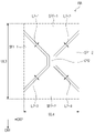
도 30은 본 발명의 일 실시예에 따른 입력감지유닛의 사시도이다.
도 31 및 도 32에서는 본 발명의 일 실시예에 따른 표시장치를 도시한 것이다.
| 제1 단위길이(UL1) | 제1 거리(L1-1, L1-2, L1-3, L1-4) | 정전용량 | |
| 실험1 | 4.333mm | 200μm | 1.003pF |
| 제3 단위길이(UL3) | 제2 거리(L2-1, L2-2, L2-3, L2-4) | 정전용량 | |
| 실험2 | 2.667mm | 75μm | 1.066pF |
| 실험3 | 2.667mm | 100μm | 1.035pF |
| 실험4 | 2.667mm | 140μm | 0.998pF |
| 제2 전극 종류 | 보조전극 조건 | 정전용량 | |
| 실험1 | 하부 제2 전극(노멀센서부) | - | 1.003pF |
| 실험2 | 상부 제2 전극(절단센서부) | - | 0.779pF |
| 실험3 | 상부 제2 전극(절단센서부) | 두께(WD) = 13μm | 1.052pF |
| 실험4 | 상부 제2 전극(절단센서부) | 두께(WD) = 100μm | 1.089pF |
| 실험5 | 상부 제2 전극(절단센서부) | 두께(WD) = 150μm | 1.106pF |
Claims (20)
- 표시패널; 및
상기 표시패널 상에 배치된 입력감지유닛을 포함하고, 상기 입력감지유닛은,
제1 방향으로 연장되는 복수의 제1 전극들; 및
상기 제1 방향과 교차하는 제2 방향으로 연장되는 복수의 제2 전극들을 포함하고,
상기 복수의 제1 전극들 각각은 복수의 제1 센서부들 및 상기 복수의 제1 센서부들을 연결하는 복수의 제1 연결부들을 포함하고,
상기 복수의 제2 전극들 각각은 복수의 제2 센서부들 및 상기 복수의 제2 센서부들을 연결하는 복수의 제2 연결부들을 포함하고,
상기 복수의 제1 전극들 중 어느 하나의 제1 전극의 상기 복수의 제1 센서부들은,
제1 면적을 가지고, 인접한 제2 센서부와 제1 거리만큼 이격된 제1 노멀센서부; 및
상기 제1 면적보다 작은 제2 면적을 가지고, 인접한 제2 센서부와 상기 제1 거리보다 작은 제2 거리만큼 이격된 제1 절단센서부를 포함하는 표시장치. - 제1 항에 있어서,
상기 제1 절단센서부는 상기 제1 노멀센서부의 일부분이 제거된 형상을 갖는 표시장치. - 제2 항에 있어서,
상기 제2 면적은 상기 제1 면적의 절반 미만 또는 절반 초과인 표시장치. - 제2 항에 있어서,
상기 어느 하나의 제1 전극의 상기 복수의 제1 센서부들은 상기 제1 노멀센서부를 복수개 포함하고,
상기 복수의 제1 노멀센서부들은 상기 제1 방향으로 나열되며,
상기 제1 절단센서부는 상기 제1 방향에서 상기 복수의 제1 노멀센서부들의 외측에 배치되는 표시장치. - 제1 항에 있어서,
상기 복수의 제1 센서들 및 상기 복수의 제2 센서들 사이에 배치되며, 상기 복수의 제1 센서들 및 상기 복수의 제2 센서들과 전기적으로 연결되지 않는 광학적 더미전극을 더 포함하고,
상기 제1 절단센서부 및 상기 제1 절단센서부에 인접한 상기 제2 센서부 사이에 배치된 상기 광학적 더미전극의 너비는 상기 제1 노멀센서부 및 상기 제1 노멀센서부에 인접한 상기 제2 센서부 사이에 배치된 상기 광학적 더미전극의 너비보다 작은 표시장치. - 제1 항에 있어서,
상기 제1 절단센서부의 일단에서 상기 제1 절단센서부에 인접한 제1 센서부의 타단까지 상기 제1 방향에서 측정한 길이는 상기 제1 노멀센서부의 일단에서 상기 제1 노멀센서부에 인접한 제1 센서부의 타단까지 상기 제1 방향에서 측정한 길이보다 작고,
상기 제1 절단센서부에 인접한 상기 제1 센서부의 면적은 상기 제1 절단센서부의 면적인 상기 제2 면적과 동일한 표시장치. - 제1 항에 있어서,
상기 복수의 제1 전극들은 상기 제1 방향에서 상기 어느 하나의 제1 전극과 길이가 다르고, 복수의 제1 센서부들을 포함하는 다른 제1 전극을 더 포함하고,
상기 다른 제1 전극의 상기 복수의 제1 센서부들은,
상기 제1 면적을 갖는 제2 노멀센서부; 및
상기 제1 면적 및 상기 제2 면적과 다른 제3 면적을 갖는 제2 절단센서부를 포함하는 표시장치. - 제7 항에 있어서,
상기 제1 절단센서부의 일단은 상기 어느 하나의 제1 전극의 상기 복수의 제1 센서부들 중 인접한 제1 센서부의 일단과 대응하는 제1 연결부에 의해 연결되고,
상기 제2 절단센서부의 일단은 상기 다른 제1 전극의 상기 복수의 제1 센서부들 중 인접한 제1 센서부의 일단과 대응하는 제1 연결부에 의해 연결되며,
상기 제1 절단센서부의 타단에서 상기 어느 하나의 제1 전극의 상기 복수의 제1 센서부들 중 상기 인접한 제1 센서부의 타단까지의 길이는 상기 제2 절단센서부의 타단에서 상기 다른 제1 전극의 상기 복수의 제1 센서부들 중 상기 인접한 제1 센서부의 타단까지의 길이보다 작은 표시장치. - 제7 항에 있어서,
상기 제3 면적은 상기 제1 면적의 절반인 표시장치. - 제1 항에 있어서,
상기 제1 절단센서부와 연결되는 보조전극을 더 포함하고, 상기 보조전극의 일측은 상기 제1 절단센서부와 인접한 상기 제2 센서부의 일측에 마주하는 표시장치. - 제10 항에 있어서,
상기 보조전극은 막대형상을 가지며, 상기 보조전극의 길이는 상기 노멀센서부의 너비보다 작은 표시장치. - 제1 항에 있어서,
상기 입력감지유닛은,
상기 복수의 제2 전극들과 연결된 복수의 신호라인들; 및
상기 제1 절단센서부에 연결되고, 상기 복수의 신호라인들과 다른 층 상에 배치되며, 상기 복수의 신호라인들 중 적어도 어느 하나의 신호라인과 중첩하는 보상전극을 더 포함하는 표시장치. - 제12 항에 있어서,
상기 보상전극과 상기 제1 절단센서부는 일체의 형상을 갖는 표시장치. - 제12 항에 있어서,
평면상에서 상기 제1 절단센서부의 일측은 곡선의 형상을 갖고,
상기 보상전극은 상기 제1 절단센서부의 상기 일측에서 연장되는 표시장치. - 제1 항에 있어서,
상기 복수의 제1 연결부들 중 인접한 제1 노멀센서부들을 연결하는 제1 연결부는 상기 제1 절단센서부 및 상기 제1 절단센서부에 인접한 제1 노멀센서부를 연결하는 제1 연결부보다 작은 너비를 가지는 표시장치. - 제15 항에 있어서,
상기 제1 절단센서부에 연결되고, 상기 복수의 제2 센서부들 중 적어도 어느 하나에 중첩하며, 제1 너비를 가지는 제1 정전기 방전 패턴; 및
상기 제1 노멀센서부에 연결되고, 상기 복수의 제2 센서부들 중 적어도 어느 하나에 중첩하며, 상기 제1 너비보다 작은 제2 너비를 가지는 제2 정전기 방전 패턴을 더 포함하는 표시장치. - 제1 항에 있어서,
상기 표시패널의 코너부들은 라운드된 형상을 갖고,
상기 입력감지유닛의 코너부들은 상기 표시패널의 상기 코너부들에 대응하는 라운드된 형상을 갖는 표시장치. - 제1 항에 있어서,
상기 입력감지유닛은 상기 복수의 제1 전극들 및 상기 복수의 제2 전극들이 배치된 감지영역 및 상기 복수의 제1 전극들 및 상기 복수의 제2 전극들이 배치되지 않은 비감지영역을 포함하고,
상기 비감지영역은 상기 감지영역의 내측에 배치되며, 상기 비감지영역과 상기 감지영역 사이에 경계가 정의되고,
상기 제1 절단센서부의 일측은 상기 경계에 대응하는 표시장치. - 제1 면적을 가지는 노멀센서부 및 상기 제1 면적의 0.05배 이상 0.45배 이하인 제2 면적을 가지는 절단센서부를 포함하는 복수의 제1 센서들; 및
상기 복수의 제1 센서부들과 교차하도록 배치되는 복수의 제2 센서들을 포함하고,
상기 노멀센서부가 인접한 제2 센서부와 형성하는 정전용량은 상기 절단센서부가 인접한 제2 센서와 형성하는 정전용량과 동일한 표시장치. - 제19 항에 있어서,
상기 절단센서부는 상기 노멀센서부의 일부분이 제거된 형상을 갖는 표시장치.
Priority Applications (5)
| Application Number | Priority Date | Filing Date | Title |
|---|---|---|---|
| KR1020170103237A KR102422074B1 (ko) | 2017-08-14 | 2017-08-14 | 표시장치 |
| US16/053,477 US10475862B2 (en) | 2017-08-14 | 2018-08-02 | Display device having an input sensing unit |
| CN201810889609.7A CN109388280B (zh) | 2017-08-14 | 2018-08-07 | 具有输入感测单元的显示装置 |
| CN202310389087.5A CN116400834A (zh) | 2017-08-14 | 2018-08-07 | 具有输入感测单元的显示装置 |
| US16/654,913 US11037996B2 (en) | 2017-08-14 | 2019-10-16 | Display device having an input sensing unit |
Applications Claiming Priority (1)
| Application Number | Priority Date | Filing Date | Title |
|---|---|---|---|
| KR1020170103237A KR102422074B1 (ko) | 2017-08-14 | 2017-08-14 | 표시장치 |
Publications (2)
| Publication Number | Publication Date |
|---|---|
| KR20190018591A KR20190018591A (ko) | 2019-02-25 |
| KR102422074B1 true KR102422074B1 (ko) | 2022-07-19 |
Family
ID=65274324
Family Applications (1)
| Application Number | Title | Priority Date | Filing Date |
|---|---|---|---|
| KR1020170103237A Active KR102422074B1 (ko) | 2017-08-14 | 2017-08-14 | 표시장치 |
Country Status (3)
| Country | Link |
|---|---|
| US (2) | US10475862B2 (ko) |
| KR (1) | KR102422074B1 (ko) |
| CN (2) | CN116400834A (ko) |
Families Citing this family (36)
| Publication number | Priority date | Publication date | Assignee | Title |
|---|---|---|---|---|
| KR102422074B1 (ko) * | 2017-08-14 | 2022-07-19 | 삼성디스플레이 주식회사 | 표시장치 |
| CN109426373B (zh) * | 2017-08-21 | 2024-08-30 | 京东方科技集团股份有限公司 | 触控面板及其制作方法、触控显示装置 |
| KR102407758B1 (ko) * | 2017-10-27 | 2022-06-10 | 엘지디스플레이 주식회사 | 터치표시장치 및 표시패널 |
| KR102488208B1 (ko) * | 2017-11-20 | 2023-01-16 | 엘지디스플레이 주식회사 | 터치 패널 및 터치 장치 |
| KR102533131B1 (ko) * | 2018-05-08 | 2023-05-18 | 삼성디스플레이 주식회사 | 입력 감지 유닛 및 이를 포함한 전자 장치 |
| KR102546769B1 (ko) * | 2018-06-08 | 2023-06-22 | 삼성디스플레이 주식회사 | 터치 센서 및 표시 장치 |
| CN108806603B (zh) * | 2018-06-29 | 2020-03-17 | 上海天马有机发光显示技术有限公司 | 一种有机发光显示面板及其驱动方法、有机发光显示装置 |
| KR102709634B1 (ko) * | 2019-03-06 | 2024-09-25 | 삼성디스플레이 주식회사 | 표시 장치 |
| KR102753281B1 (ko) * | 2019-04-24 | 2025-01-15 | 삼성디스플레이 주식회사 | 터치 센서 및 이를 포함하는 표시 장치 |
| KR102771912B1 (ko) * | 2019-04-29 | 2025-02-26 | 삼성디스플레이 주식회사 | 입력감지회로 및 이를 포함하는 표시모듈 |
| CN110148592B (zh) * | 2019-05-21 | 2020-12-11 | 上海天马有机发光显示技术有限公司 | 一种显示面板、包含其的显示装置 |
| KR102787862B1 (ko) * | 2019-07-11 | 2025-04-01 | 삼성디스플레이 주식회사 | 표시 장치 |
| JP2021034261A (ja) * | 2019-08-27 | 2021-03-01 | 株式会社ジャパンディスプレイ | 表示装置 |
| US11354002B2 (en) * | 2019-09-04 | 2022-06-07 | Samsung Display Co., Ltd. | Touch sensing unit and display device including the same |
| US12008191B2 (en) * | 2019-10-09 | 2024-06-11 | Novatek Microelectronics Corp. | Single-chip device for driving a panel including fingerprint sensing pixels, display pixels and touch sensors, electronic module therefor, and electronic apparatus including the single-chip device |
| KR102951617B1 (ko) | 2019-11-22 | 2026-04-14 | 삼성디스플레이 주식회사 | 표시장치 |
| KR102858762B1 (ko) | 2019-12-20 | 2025-09-10 | 엘지디스플레이 주식회사 | 카메라 투과부를 포함하는 표시 장치 |
| KR102787004B1 (ko) | 2020-02-21 | 2025-03-26 | 삼성디스플레이 주식회사 | 표시 장치 |
| CN211044880U (zh) * | 2020-03-13 | 2020-07-17 | 京东方科技集团股份有限公司 | 显示装置、线路板组件 |
| KR102949658B1 (ko) * | 2020-04-16 | 2026-04-09 | 삼성디스플레이 주식회사 | 표시 패널 및 표시 장치 |
| CN111831157B (zh) * | 2020-07-14 | 2024-03-19 | 京东方科技集团股份有限公司 | 一种触控显示面板及其驱动方法、触控显示装置 |
| KR102903801B1 (ko) * | 2020-08-14 | 2025-12-26 | 삼성디스플레이 주식회사 | 표시장치 |
| KR102819456B1 (ko) * | 2020-10-16 | 2025-06-16 | 삼성디스플레이 주식회사 | 전자장치 및 이의 검사방법 |
| KR102929015B1 (ko) * | 2020-10-19 | 2026-02-24 | 삼성디스플레이 주식회사 | 터치 센서 및 이를 포함하는 표시 장치 |
| KR20220075110A (ko) * | 2020-11-27 | 2022-06-07 | 삼성디스플레이 주식회사 | 표시장치 |
| US12096657B2 (en) | 2020-12-07 | 2024-09-17 | Apple Inc. | Display circuitry with semiconducting oxide transistors |
| DE102020134390A1 (de) * | 2020-12-21 | 2022-06-23 | Marquardt Gmbh | Anordnung zur ortsauflösenden projiziert-kapazitiven Berührdetektion mit nicht modifizierter Umfangsoptimierung an Durchbrüchen |
| DE102020134394A1 (de) * | 2020-12-21 | 2022-06-23 | Marquardt Gmbh | Anordnung zur ortsauflösenden projiziert-kapazitiven Berührdetektion mit lichtdurchlässigem Substrat |
| TWI771095B (zh) * | 2021-07-05 | 2022-07-11 | 星河半導體股份有限公司 | 感應面板的控制晶片、控制電路及控制方法 |
| KR20230020045A (ko) * | 2021-08-02 | 2023-02-10 | 삼성디스플레이 주식회사 | 터치 감지부 및 이를 포함하는 표시 장치 |
| CN114115588B (zh) * | 2021-09-26 | 2023-11-03 | 洛晶半导体(上海)有限公司 | 感应面板的控制芯片、控制电路及控制方法 |
| KR20230046341A (ko) | 2021-09-29 | 2023-04-06 | 삼성디스플레이 주식회사 | 터치 감지부 및 이를 포함하는 표시 장치 |
| KR20230063924A (ko) * | 2021-10-29 | 2023-05-10 | 삼성디스플레이 주식회사 | 전자 장치 |
| KR20230082167A (ko) | 2021-12-01 | 2023-06-08 | 엘지디스플레이 주식회사 | 터치패널 및 이를 포함하는 터치표시장치 |
| US20240054940A1 (en) * | 2022-08-12 | 2024-02-15 | Samsung Display Co., Ltd. | Display device |
| KR20240141005A (ko) * | 2023-03-15 | 2024-09-25 | 삼성디스플레이 주식회사 | 센서층 및 이를 포함하는 전자 장치 |
Citations (1)
| Publication number | Priority date | Publication date | Assignee | Title |
|---|---|---|---|---|
| KR100978461B1 (ko) | 2008-07-04 | 2010-08-26 | 안영수 | 고감도 디지탈방식의 정전용량터치패널장치 |
Family Cites Families (17)
| Publication number | Priority date | Publication date | Assignee | Title |
|---|---|---|---|---|
| JP5252454B2 (ja) * | 2009-06-30 | 2013-07-31 | 株式会社ジャパンディスプレイウェスト | 接触検出装置、および、タッチセンサ機能を有する表示装置 |
| TWI498786B (zh) * | 2009-08-24 | 2015-09-01 | Semiconductor Energy Lab | 觸控感應器及其驅動方法與顯示裝置 |
| US8970509B2 (en) * | 2009-12-09 | 2015-03-03 | Lg Display Co., Ltd. | Touch panel and liquid crystal display device including the same |
| KR20130044432A (ko) | 2011-10-24 | 2013-05-03 | 주식회사 트레이스 | 정전용량 방식의 터치스크린에서 가장자리 부분의 출력 좌표 보강을 위한 센서 패턴 |
| KR101768940B1 (ko) | 2013-05-16 | 2017-08-17 | 미쓰비시 세이시 가부시키가이샤 | 도전성 패턴 및 단층 정전용량 방식 터치패널의 전극패턴 |
| KR102096622B1 (ko) * | 2013-08-19 | 2020-04-03 | 삼성디스플레이 주식회사 | 유기발광 표시장치 |
| KR102112818B1 (ko) * | 2013-09-03 | 2020-05-19 | 동우 화인켐 주식회사 | 터치 감지 전극 및 이를 구비하는 터치 스크린 패널 |
| KR102029489B1 (ko) | 2014-07-22 | 2019-10-07 | 삼성전기주식회사 | 박막 인덕터용 코일 유닛, 박막 인덕터용 코일 유닛의 제조방법, 박막 인덕터 및 박막 인덕터의 제조방법 |
| KR102219186B1 (ko) * | 2014-08-06 | 2021-02-22 | 엘지디스플레이 주식회사 | 터치 스크린 일체형 유기 발광 표시 장치 및 터치 스크린 일체형 유기 발광 표시 장치 제조 방법 |
| KR102239861B1 (ko) | 2014-11-26 | 2021-04-13 | 삼성디스플레이 주식회사 | 터치 센서를 포함하는 표시 장치 및 그 구동 방법 |
| KR102264760B1 (ko) * | 2014-11-26 | 2021-06-14 | 삼성디스플레이 주식회사 | 터치 센서를 포함하는 표시 장치 및 그 제조 방법 |
| KR102267357B1 (ko) | 2014-12-15 | 2021-06-21 | 삼성디스플레이 주식회사 | 터치 센서 장치 |
| KR102195392B1 (ko) | 2015-03-27 | 2020-12-24 | 동우 화인켐 주식회사 | 터치패널 |
| KR102568864B1 (ko) * | 2015-06-26 | 2023-08-23 | 삼성디스플레이 주식회사 | 플렉서블 표시장치 |
| KR102598155B1 (ko) | 2016-10-27 | 2023-11-07 | 삼성디스플레이 주식회사 | 전자 장치 |
| KR102333396B1 (ko) * | 2017-06-01 | 2021-11-30 | 엘지디스플레이 주식회사 | 터치 디스플레이 장치 및 터치 디스플레이 패널 |
| KR102422074B1 (ko) * | 2017-08-14 | 2022-07-19 | 삼성디스플레이 주식회사 | 표시장치 |
-
2017
- 2017-08-14 KR KR1020170103237A patent/KR102422074B1/ko active Active
-
2018
- 2018-08-02 US US16/053,477 patent/US10475862B2/en active Active
- 2018-08-07 CN CN202310389087.5A patent/CN116400834A/zh active Pending
- 2018-08-07 CN CN201810889609.7A patent/CN109388280B/zh active Active
-
2019
- 2019-10-16 US US16/654,913 patent/US11037996B2/en active Active
Patent Citations (1)
| Publication number | Priority date | Publication date | Assignee | Title |
|---|---|---|---|---|
| KR100978461B1 (ko) | 2008-07-04 | 2010-08-26 | 안영수 | 고감도 디지탈방식의 정전용량터치패널장치 |
Also Published As
| Publication number | Publication date |
|---|---|
| US11037996B2 (en) | 2021-06-15 |
| CN116400834A (zh) | 2023-07-07 |
| US20200052044A1 (en) | 2020-02-13 |
| KR20190018591A (ko) | 2019-02-25 |
| US10475862B2 (en) | 2019-11-12 |
| US20190051708A1 (en) | 2019-02-14 |
| CN109388280A (zh) | 2019-02-26 |
| CN109388280B (zh) | 2023-04-28 |
Similar Documents
| Publication | Publication Date | Title |
|---|---|---|
| KR102422074B1 (ko) | 표시장치 | |
| KR102386894B1 (ko) | 표시장치 및 그 제조방법 | |
| KR102750120B1 (ko) | 표시 장치 | |
| KR102745931B1 (ko) | 표시장치 | |
| KR102521879B1 (ko) | 표시장치 | |
| US20230031525A1 (en) | Display device | |
| KR102351618B1 (ko) | 표시장치 | |
| KR102606941B1 (ko) | 표시장치 | |
| TWI806956B (zh) | 觸控感測器及包含其的顯示裝置 | |
| KR102377527B1 (ko) | 입력감지유닛 및 이를 구비한 표시장치 | |
| EP3333683B1 (en) | Display module | |
| KR20240172161A (ko) | 표시장치 | |
| KR102418609B1 (ko) | 표시장치 | |
| KR20200060601A (ko) | 입력감지유닛 및 이를 포함하는 표시장치 | |
| KR102737591B1 (ko) | 표시장치 |
Legal Events
| Date | Code | Title | Description |
|---|---|---|---|
| PA0109 | Patent application |
St.27 status event code: A-0-1-A10-A12-nap-PA0109 |
|
| R18-X000 | Changes to party contact information recorded |
St.27 status event code: A-3-3-R10-R18-oth-X000 |
|
| PG1501 | Laying open of application |
St.27 status event code: A-1-1-Q10-Q12-nap-PG1501 |
|
| A201 | Request for examination | ||
| PA0201 | Request for examination |
St.27 status event code: A-1-2-D10-D11-exm-PA0201 |
|
| E902 | Notification of reason for refusal | ||
| PE0902 | Notice of grounds for rejection |
St.27 status event code: A-1-2-D10-D21-exm-PE0902 |
|
| P11-X000 | Amendment of application requested |
St.27 status event code: A-2-2-P10-P11-nap-X000 |
|
| P13-X000 | Application amended |
St.27 status event code: A-2-2-P10-P13-nap-X000 |
|
| E701 | Decision to grant or registration of patent right | ||
| PE0701 | Decision of registration |
St.27 status event code: A-1-2-D10-D22-exm-PE0701 |
|
| GRNT | Written decision to grant | ||
| PR0701 | Registration of establishment |
St.27 status event code: A-2-4-F10-F11-exm-PR0701 |
|
| PR1002 | Payment of registration fee |
St.27 status event code: A-2-2-U10-U11-oth-PR1002 Fee payment year number: 1 |
|
| PG1601 | Publication of registration |
St.27 status event code: A-4-4-Q10-Q13-nap-PG1601 |
|
| P22-X000 | Classification modified |
St.27 status event code: A-4-4-P10-P22-nap-X000 |
|
| P22-X000 | Classification modified |
St.27 status event code: A-4-4-P10-P22-nap-X000 |
|
| PR1001 | Payment of annual fee |
St.27 status event code: A-4-4-U10-U11-oth-PR1001 Fee payment year number: 4 |
|
| P22-X000 | Classification modified |
St.27 status event code: A-4-4-P10-P22-nap-X000 |