KR102195552B1 - Gate driver for switching converter having body diode power loss minimization - Google Patents
Gate driver for switching converter having body diode power loss minimization Download PDFInfo
- Publication number
- KR102195552B1 KR102195552B1 KR1020190017372A KR20190017372A KR102195552B1 KR 102195552 B1 KR102195552 B1 KR 102195552B1 KR 1020190017372 A KR1020190017372 A KR 1020190017372A KR 20190017372 A KR20190017372 A KR 20190017372A KR 102195552 B1 KR102195552 B1 KR 102195552B1
- Authority
- KR
- South Korea
- Prior art keywords
- transistor
- low
- gate
- side transistor
- current
- Prior art date
- Legal status (The legal status is an assumption and is not a legal conclusion. Google has not performed a legal analysis and makes no representation as to the accuracy of the status listed.)
- Active
Links
Images


Classifications
-
- H—ELECTRICITY
- H02—GENERATION; CONVERSION OR DISTRIBUTION OF ELECTRIC POWER
- H02M—APPARATUS FOR CONVERSION BETWEEN AC AND AC, BETWEEN AC AND DC, OR BETWEEN DC AND DC, AND FOR USE WITH MAINS OR SIMILAR POWER SUPPLY SYSTEMS; CONVERSION OF DC OR AC INPUT POWER INTO SURGE OUTPUT POWER; CONTROL OR REGULATION THEREOF
- H02M7/00—Conversion of AC power input into DC power output; Conversion of DC power input into AC power output
- H02M7/42—Conversion of DC power input into AC power output without possibility of reversal
- H02M7/44—Conversion of DC power input into AC power output without possibility of reversal by static converters
- H02M7/48—Conversion of DC power input into AC power output without possibility of reversal by static converters using discharge tubes with control electrode or semiconductor devices with control electrode
- H02M7/53—Conversion of DC power input into AC power output without possibility of reversal by static converters using discharge tubes with control electrode or semiconductor devices with control electrode using devices of a triode or transistor type requiring continuous application of a control signal
- H02M7/537—Conversion of DC power input into AC power output without possibility of reversal by static converters using discharge tubes with control electrode or semiconductor devices with control electrode using devices of a triode or transistor type requiring continuous application of a control signal using semiconductor devices only, e.g. single switched pulse inverters
- H02M7/539—Conversion of DC power input into AC power output without possibility of reversal by static converters using discharge tubes with control electrode or semiconductor devices with control electrode using devices of a triode or transistor type requiring continuous application of a control signal using semiconductor devices only, e.g. single switched pulse inverters with automatic control of output wave form or frequency
- H02M7/5395—Conversion of DC power input into AC power output without possibility of reversal by static converters using discharge tubes with control electrode or semiconductor devices with control electrode using devices of a triode or transistor type requiring continuous application of a control signal using semiconductor devices only, e.g. single switched pulse inverters with automatic control of output wave form or frequency by pulse-width modulation
-
- H—ELECTRICITY
- H02—GENERATION; CONVERSION OR DISTRIBUTION OF ELECTRIC POWER
- H02M—APPARATUS FOR CONVERSION BETWEEN AC AND AC, BETWEEN AC AND DC, OR BETWEEN DC AND DC, AND FOR USE WITH MAINS OR SIMILAR POWER SUPPLY SYSTEMS; CONVERSION OF DC OR AC INPUT POWER INTO SURGE OUTPUT POWER; CONTROL OR REGULATION THEREOF
- H02M1/00—Details of apparatus for conversion
- H02M1/08—Circuits specially adapted for the generation of control voltages for semiconductor devices incorporated in static converters
- H02M1/088—Circuits specially adapted for the generation of control voltages for semiconductor devices incorporated in static converters for the simultaneous control of series or parallel connected semiconductor devices
-
- H—ELECTRICITY
- H02—GENERATION; CONVERSION OR DISTRIBUTION OF ELECTRIC POWER
- H02M—APPARATUS FOR CONVERSION BETWEEN AC AND AC, BETWEEN AC AND DC, OR BETWEEN DC AND DC, AND FOR USE WITH MAINS OR SIMILAR POWER SUPPLY SYSTEMS; CONVERSION OF DC OR AC INPUT POWER INTO SURGE OUTPUT POWER; CONTROL OR REGULATION THEREOF
- H02M7/00—Conversion of AC power input into DC power output; Conversion of DC power input into AC power output
- H02M7/42—Conversion of DC power input into AC power output without possibility of reversal
- H02M7/44—Conversion of DC power input into AC power output without possibility of reversal by static converters
- H02M7/48—Conversion of DC power input into AC power output without possibility of reversal by static converters using discharge tubes with control electrode or semiconductor devices with control electrode
- H02M7/53—Conversion of DC power input into AC power output without possibility of reversal by static converters using discharge tubes with control electrode or semiconductor devices with control electrode using devices of a triode or transistor type requiring continuous application of a control signal
- H02M7/537—Conversion of DC power input into AC power output without possibility of reversal by static converters using discharge tubes with control electrode or semiconductor devices with control electrode using devices of a triode or transistor type requiring continuous application of a control signal using semiconductor devices only, e.g. single switched pulse inverters
- H02M7/5387—Conversion of DC power input into AC power output without possibility of reversal by static converters using discharge tubes with control electrode or semiconductor devices with control electrode using devices of a triode or transistor type requiring continuous application of a control signal using semiconductor devices only, e.g. single switched pulse inverters in a bridge configuration
-
- H—ELECTRICITY
- H03—ELECTRONIC CIRCUITRY
- H03K—PULSE TECHNIQUE
- H03K17/00—Electronic switching or gating, i.e. not by contact-making and –breaking
- H03K17/06—Modifications for ensuring a fully conducting state
- H03K17/063—Modifications for ensuring a fully conducting state in field-effect transistor switches
-
- H—ELECTRICITY
- H03—ELECTRONIC CIRCUITRY
- H03K—PULSE TECHNIQUE
- H03K17/00—Electronic switching or gating, i.e. not by contact-making and –breaking
- H03K17/08—Modifications for protecting switching circuit against overcurrent or overvoltage
- H03K17/082—Modifications for protecting switching circuit against overcurrent or overvoltage by feedback from the output to the control circuit
- H03K17/0822—Modifications for protecting switching circuit against overcurrent or overvoltage by feedback from the output to the control circuit in field-effect transistor switches
-
- H—ELECTRICITY
- H03—ELECTRONIC CIRCUITRY
- H03K—PULSE TECHNIQUE
- H03K17/00—Electronic switching or gating, i.e. not by contact-making and –breaking
- H03K17/16—Modifications for eliminating interference voltages or currents
- H03K17/161—Modifications for eliminating interference voltages or currents in field-effect transistor switches
- H03K17/162—Modifications for eliminating interference voltages or currents in field-effect transistor switches without feedback from the output circuit to the control circuit
-
- H—ELECTRICITY
- H03—ELECTRONIC CIRCUITRY
- H03K—PULSE TECHNIQUE
- H03K17/00—Electronic switching or gating, i.e. not by contact-making and –breaking
- H03K17/16—Modifications for eliminating interference voltages or currents
- H03K17/161—Modifications for eliminating interference voltages or currents in field-effect transistor switches
- H03K17/165—Modifications for eliminating interference voltages or currents in field-effect transistor switches by feedback from the output circuit to the control circuit
- H03K17/166—Soft switching
-
- H—ELECTRICITY
- H03—ELECTRONIC CIRCUITRY
- H03K—PULSE TECHNIQUE
- H03K17/00—Electronic switching or gating, i.e. not by contact-making and –breaking
- H03K17/51—Electronic switching or gating, i.e. not by contact-making and –breaking characterised by the components used
- H03K17/56—Electronic switching or gating, i.e. not by contact-making and –breaking characterised by the components used by the use, as active elements, of semiconductor devices
- H03K17/687—Electronic switching or gating, i.e. not by contact-making and –breaking characterised by the components used by the use, as active elements, of semiconductor devices the devices being field-effect transistors
-
- H—ELECTRICITY
- H03—ELECTRONIC CIRCUITRY
- H03K—PULSE TECHNIQUE
- H03K3/00—Circuits for generating electric pulses; Monostable, bistable or multistable circuits
- H03K3/01—Details
- H03K3/012—Modifications of generator to improve response time or to decrease power consumption
-
- H—ELECTRICITY
- H02—GENERATION; CONVERSION OR DISTRIBUTION OF ELECTRIC POWER
- H02M—APPARATUS FOR CONVERSION BETWEEN AC AND AC, BETWEEN AC AND DC, OR BETWEEN DC AND DC, AND FOR USE WITH MAINS OR SIMILAR POWER SUPPLY SYSTEMS; CONVERSION OF DC OR AC INPUT POWER INTO SURGE OUTPUT POWER; CONTROL OR REGULATION THEREOF
- H02M1/00—Details of apparatus for conversion
- H02M1/0048—Circuits or arrangements for reducing losses
- H02M1/0051—Diode reverse recovery losses
-
- H—ELECTRICITY
- H02—GENERATION; CONVERSION OR DISTRIBUTION OF ELECTRIC POWER
- H02M—APPARATUS FOR CONVERSION BETWEEN AC AND AC, BETWEEN AC AND DC, OR BETWEEN DC AND DC, AND FOR USE WITH MAINS OR SIMILAR POWER SUPPLY SYSTEMS; CONVERSION OF DC OR AC INPUT POWER INTO SURGE OUTPUT POWER; CONTROL OR REGULATION THEREOF
- H02M1/00—Details of apparatus for conversion
- H02M1/0048—Circuits or arrangements for reducing losses
- H02M1/0054—Transistor switching losses
- H02M1/0058—Transistor switching losses by employing soft switching techniques, i.e. commutation of transistors when applied voltage is zero or when current flow is zero
-
- H—ELECTRICITY
- H03—ELECTRONIC CIRCUITRY
- H03K—PULSE TECHNIQUE
- H03K17/00—Electronic switching or gating, i.e. not by contact-making and –breaking
- H03K17/04—Modifications for accelerating switching
- H03K17/041—Modifications for accelerating switching without feedback from the output circuit to the control circuit
- H03K17/0412—Modifications for accelerating switching without feedback from the output circuit to the control circuit by measures taken in the control circuit
- H03K17/04123—Modifications for accelerating switching without feedback from the output circuit to the control circuit by measures taken in the control circuit in field-effect transistor switches
-
- H—ELECTRICITY
- H03—ELECTRONIC CIRCUITRY
- H03K—PULSE TECHNIQUE
- H03K2217/00—Indexing scheme related to electronic switching or gating, i.e. not by contact-making or -breaking covered by H03K17/00
- H03K2217/0063—High side switches, i.e. the higher potential [DC] or life wire [AC] being directly connected to the switch and not via the load
-
- H—ELECTRICITY
- H03—ELECTRONIC CIRCUITRY
- H03K—PULSE TECHNIQUE
- H03K2217/00—Indexing scheme related to electronic switching or gating, i.e. not by contact-making or -breaking covered by H03K17/00
- H03K2217/0072—Low side switches, i.e. the lower potential [DC] or neutral wire [AC] being directly connected to the switch and not via the load
-
- Y—GENERAL TAGGING OF NEW TECHNOLOGICAL DEVELOPMENTS; GENERAL TAGGING OF CROSS-SECTIONAL TECHNOLOGIES SPANNING OVER SEVERAL SECTIONS OF THE IPC; TECHNICAL SUBJECTS COVERED BY FORMER USPC CROSS-REFERENCE ART COLLECTIONS [XRACs] AND DIGESTS
- Y02—TECHNOLOGIES OR APPLICATIONS FOR MITIGATION OR ADAPTATION AGAINST CLIMATE CHANGE
- Y02B—CLIMATE CHANGE MITIGATION TECHNOLOGIES RELATED TO BUILDINGS, e.g. HOUSING, HOUSE APPLIANCES OR RELATED END-USER APPLICATIONS
- Y02B70/00—Technologies for an efficient end-user side electric power management and consumption
- Y02B70/10—Technologies improving the efficiency by using switched-mode power supplies [SMPS], i.e. efficient power electronics conversion e.g. power factor correction or reduction of losses in power supplies or efficient standby modes
Landscapes
- Engineering & Computer Science (AREA)
- Power Engineering (AREA)
- Power Conversion In General (AREA)
- Electronic Switches (AREA)
- Inverter Devices (AREA)
Abstract
유도성 부하를 갖는 스위칭 컨버터에서, 트랜지스터의 게이트가 트랜지스터를 오프로 유지하도록 제어되더라도, 전류는 트랜지스터의 바디 다이오드를 통해 흐를 수 있다. 그리고, 스위치 레그의 다른 트랜지스터가 온 되면 리버스 리커버리 전류가 바디 다이오드를 통해 역방향으로 흐른다. 이러한 전류 흐름과 연관된 스위칭 손실을 줄이기 위해 게이트 드라이버 집적 회로는 바디 다이오드를 통과하는 전류 흐름이 임계 전류 이상으로 상승할 때이를 감지한다. 게이트 드라이버 집적 회로는 트랜지스터가 온 되도록 제어한다. 그리고, 스위치 레그의 다른 트랜지스터가 켜지게 되면 게이트 드라이버는 먼저 트랜지스터를 오프 한다. 오프 트랜지스터의 게이트-소스 전압이 임계 전압 아래로 떨어지면, 게이트 드라이버 집적 회로는 다른 트랜지스터가 턴 온 되도록 허용하고 제어한다.In a switching converter with an inductive load, even if the gate of the transistor is controlled to keep the transistor off, current can flow through the body diode of the transistor. In addition, when the other transistor of the switch leg is turned on, a reverse recovery current flows in the reverse direction through the body diode. To reduce the switching losses associated with this current flow, the gate driver integrated circuit detects when the current flow through the body diode rises above a threshold current. The gate driver integrated circuit controls the transistor to be turned on. And, when the other transistor of the switch leg is turned on, the gate driver first turns off the transistor. When the gate-source voltage of the off transistor falls below the threshold voltage, the gate driver integrated circuit allows and controls the other transistor to turn on.
Description
기재된 실시예는 전력 전계 효과 트랜지스터(소위, MOSFETs)와 같은 전력 트랜지스터의 게이트를 구동하기 위한 게이트 드라이버에 관한 것이다.The described embodiment relates to a gate driver for driving the gate of a power transistor, such as power field effect transistors (so-called MOSFETs).
스위칭 전력 컨버터(switching converter)에는 몇 가지 유형의 전력 손실이 존재한다. 이를 설명하기 위하여, 여기서는 하나의 특정 유형의 스위칭 컨버터에 대해 간략하게 설명한다. 일반적으로 "인버터(inverter)" 라고 하는 DC-to-AC 스위칭 컨버터이다. 인버터는 DC 공급 전압을 수신하여 정현파(sinusoidal) AC 전압 또는 전류를 출력한다. 인버터에 대한 다양한 회로 토폴로지(topology)가 있지만, 도 1a는 하나의 예시적인 인버터 회로의 일부의 일 예를 도시한다. 인버터 회로에는 QHS 라고 하는 소위 "하이 사이드(high-side)" 트랜지스터와 QLS 라고 하는 소위 "로우 사이드(low-side)" 트랜지스터가 포함된다. 이들 각각의 트랜지스터는 N 채널 MOSFET(Metal-Oxide Semiconductor Field Effect Transistor)라고 불리는 N 채널 전계 효과 트랜지스터이다. 이들 각각의 트랜지스터는 반도체 다이(die)의 일부분에 구현된다. 반도체 다이의 일부인 내재된(inherent) 바디 다이오드(body diode)가 있다. 다이오드는 N 채널 트랜지스터의 기호로 예시될 수 있거나 전혀 도시되지 않을 수 있지만, 트랜지스터와 함께 존재한다. 인버터 회로에서, 노드(node) N1 상에 존재하는 제1 DC 공급 전압(first DC supply voltage) 및 노드 N2 상에 존재하는 제2의 더 높은 DC 공급 전압(second higher DC supply voltage)이 존재한다. 노드 GND는 접지 노드이다. 도면 부호 L은 변압기의 제1 권선(winding)(1 차측 권선)을 나타낸다. 변압기의 코어(core) 및 변압기의 제2 권선(2 차측 권선)은 도시되지 않았다. 인버터 회로의 전체적인 목적은 제1 권선 L을 통하여 AC 전류 흐름을 생성하는 것이다. 이것은 변압기의 제2 권선에 유사한 AC 전류를 흐르게 하고, 제2 권선의 이 AC 전류는 부하를 통과하게 된다. 하이 사이드 및 로우 사이드 트랜지스터를 제어하는 제어 및 드라이 회로는 도시하지 않았다.There are several types of power losses in switching converters. To illustrate this, here is a brief description of one specific type of switching converter. It is a DC-to-AC switching converter, commonly referred to as "inverter". The inverter receives the DC supply voltage and outputs a sinusoidal AC voltage or current. Although there are various circuit topologies for inverters, FIG. 1A shows an example of a portion of one exemplary inverter circuit. The inverter circuit includes a so-called "high-side" transistor called QHS and a so-called "low-side" transistor called QLS. Each of these transistors is an N-channel field effect transistor called an N-channel MOSFET (Metal-Oxide Semiconductor Field Effect Transistor). Each of these transistors is implemented on a portion of a semiconductor die. There is an inherent body diode that is part of a semiconductor die. The diode may be illustrated by the symbol of an N-channel transistor or not shown at all, but is present with the transistor. In the inverter circuit, there is a first DC supply voltage present on node N1 and a second higher DC supply voltage present on node N2. Node GND is a ground node. Reference numeral L denotes a first winding (primary winding) of the transformer. The core of the transformer and the secondary winding of the transformer (secondary winding) are not shown. The overall purpose of the inverter circuit is to create an AC current flow through the first winding L. This causes a similar AC current to flow in the second winding of the transformer, and this AC current in the second winding passes through the load. Control and dry circuits for controlling the high side and low side transistors are not shown.
권선 L에 흐르는 출력 정현파 AC 전류 흐름의 첫번째 반주기(half cycle)에서, 하이 사이드 트랜지스터(high-side transistor)는 오프(off)로 제어된다. 이것은 도 1a, 도 1b, 도 1c 및 도 1d에서 하이 사이드 트랜지스터 QHS에 의해 나타나는 "OFF"의 기재로 표시된다. 한편, 로우 사이드 트랜지스터(low-side transistor) QLS는 정현파 AC 전류가 제1 권선을 통해 흐르게 하는 방식으로 스위치 온 및 오프 된다. 그 다음, 정현파 AC 전류 흐름의 두번째 반주기에서 로우 사이드 트랜지스터 QLS는 오프로 제어된다. 이 두번째 반주기에서 인버터 회로의 동작은 도시되지 않았다. 정현파 AC 전류 흐름의 두번째 반주기에서, 하이 사이드 트랜지스터 QHS는 정현파 AC 전류가 흐르도록 하는 방식으로 스위치 온 및 오프 된다.In the first half cycle of the output sinusoidal AC current flow through winding L, the high-side transistor is controlled off. This is indicated by the description of "OFF" indicated by the high side transistor QHS in Figs. 1A, 1B, 1C and 1D. Meanwhile, the low-side transistor QLS is switched on and off in a manner that allows a sinusoidal AC current to flow through the first winding. Then, in the second half cycle of the sinusoidal AC current flow, the low side transistor QLS is controlled to off. The operation of the inverter circuit in this second half cycle is not shown. In the second half cycle of the sinusoidal AC current flow, the high side transistor QHS is switched on and off in such a way that the sinusoidal AC current flows.
도 1a, 도 1b, 도 1c 및 도 1d는 정현파 AC 전류의 예시적인 첫번째 반주기(half cycle) 동안의 전류 흐름을 도시한다. 도 1a는 첫번째 상황을 도시한다. 로우 사이드 트랜지스터 QLS는 온(on)으로 제어된다. 전류는 화살표 A로 도시된 바와 같이 흐르게 된다. 전류는 노드 N1으로부터 권선 L을 통해 트랜지스터 QLS를 통해 그리고 접지 노드 GND로 흐른다. 일정 기간 후에, 로우 사이드 트랜지스터 QLS가 턴 오프(turn off) 된다. 이는 도 1b에 도시된 상황을 발생시킨다. 전류는 제1 권선 L의 인덕턴스에서 순간적으로 정지할 수 없으며, 또한 블로킹된 로우 사이드 트랜지스터 QLS를 통해 흐를 수 없기 때문에, 화살표 B로 도시된 경로를 흐른다. 하이 사이드 트랜지스터 QHS는 오프이지만, 전류(B)는 바디 다이오드(body diode) DHS를 통해 노드(N2)까지 흐른다. 시간이 경과하면, 로우 사이드 트랜지스터 QLS가 다시 턴 온(turn on) 된다. 전류는 도 1c의 화살표 C로 도시된 바와 같이 흐른다. 로우 사이드 트랜지스터 QLS는 온 되어 전도 상태가 되므로, 전류가 노드 N1로부터 권선 L을 통해서, 로우 사이드 트랜지스터 QLS를 통해서, 그리고 접지 노드 GND로 흐른다. 그러나, 로우 사이드 트랜지스터 QLS가 처음으로 턴 온 되면, 하이 사이드 트랜지스터의 바디 다이오드 DHS에 역 전압이 인가된다. 이로 인하여, 바디 다이오드 DHS를 통해 흐르는 리버스 리커버리 전류(reverse recovery current)에 짧은 파열(burst)이 발생된다. 이 리버스 리커버리 전류의 파열은 도 1c에 도시된 경로 C를 따라 흐른다. 이 리버스 리커버리 전류의 흐름이 정지하게 되면, 도 1d에 도시한 바와 같이 된다. 1A, 1B, 1C and 1D show current flow during an exemplary first half cycle of a sinusoidal AC current. 1A shows the first situation. The low-side transistor QLS is controlled to be on. Current flows as shown by arrow A. Current flows from node N1 through winding L through transistor QLS and to ground node GND. After a period of time, the low side transistor QLS is turned off. This causes the situation shown in Fig. 1B. Since the current cannot stop momentarily at the inductance of the first winding L and also cannot flow through the blocked low side transistor QLS, it flows through the path shown by arrow B. The high side transistor QHS is off, but the current B flows through the body diode DHS to the node N2. As time passes, the low-side transistor QLS is turned on again. Current flows as shown by arrow C in Fig. 1C. Since the low-side transistor QLS is on and in a conducting state, current flows from node N1 through winding L, through the low-side transistor QLS, and to the ground node GND. However, when the low-side transistor QLS is turned on for the first time, a reverse voltage is applied to the body diode DHS of the high-side transistor. Due to this, a short burst occurs in the reverse recovery current flowing through the body diode DHS. The rupture of this reverse recovery current flows along the path C shown in Fig. 1C. When the flow of this reverse recovery current stops, it becomes as shown in Fig. 1D.
바디 다이오드 DHS를 통한 전류 흐름은 스위칭 컨버터에서 전력 손실을 일으킬 수 있다. 상대적으로 짧은 지속 기간 임에도 불구하고, 도 1c에 도시된 리버스 리커버리 전류의 서지(serge)는 큰 전류이며, 큰 역전압이 바디 다이오드 양단에 인가되는 시간 동안 발생한다. 바디 다이오드 DHS를 통하는 순간 전류(instantaneous current) 흐름에 대한 시간에 따른 적분과 바디 다이오드 DHS의 순간 전압 강하(instantaneous voltage drop)를 곱한 값은 에너지 손실을 나타낸다. 이것은 리버스 리커버리 전류(reverse recovery current)의 흐름으로 인한 에너지 손실이다. 또한, 바디 다이오드 DHS를 통한 순방향 전류 흐름으로 인한 에너지 손실이 있다. 도 1b에 도시된 전류(B)가 바디 다이오드 DHS를 가로 질러 흐를 때, 바디 다이오드 DHS 양단에 약 1 볼트 전압 강하가 존재한다. 바디 다이오드 DHS를 통과하는 순간 전류 흐름의 총합에 바디 다이오드 DHS 양단의 순간 전압 강하를 곱하면 에너지 손실을 나타낸다.Current flow through the body diode DHS can cause power loss in the switching converter. Despite the relatively short duration, the surge (serge) of the reverse recovery current shown in FIG. 1C is a large current, and occurs during a time when a large reverse voltage is applied across the body diode. The time-dependent integral of the instantaneous current flow through the body diode DHS multiplied by the instantaneous voltage drop of the body diode DHS represents the energy loss. This is the energy loss due to the flow of reverse recovery current. Also, there is an energy loss due to the forward current flow through the body diode DHS. When the current B shown in FIG. 1B flows across the body diode DHS, there is a voltage drop of about 1 volt across the body diode DHS. Energy loss is obtained by multiplying the sum of the instantaneous current flow through the body diode DHS by the instantaneous voltage drop across the body diode DHS.
하나의 새로운 양태에서, 게이트 드라이버 집적 회로(gate driver integrated circuit)는 하이 사이드 게이트 드라이버(high-side gate driver) 및 로우 사이드 게이트 드라이버(low-side gate driver)를 갖는다. 게이트 드라이버 집적 회로는 DC-to-AC 인버터 회로의 하이 사이드 N 채널 전계 효과 트랜지스터(high-side N-channel field effect transistor) 및 로우 사이드 N 채널 전계 효과 트랜지스터(low-side N-channel field effect transistor)를 제어한다. 하이 사이드 트랜지스터 및 로우 사이드 트랜지스터는 스위칭 레그(switching leg) 또는 위상 레그(phase-leg) 회로의 부품이다. 하이 사이드 트랜지스터의 소스는 중앙 스위칭 노드 SW에서 로우 사이드 트랜지스터의 드레인에 연결된다. 또한, 대형 인덕터 또는 변압기 권선의 일측 단부는 중앙 스위칭 노드 SW에 연결된다.In one new aspect, the gate driver integrated circuit has a high-side gate driver and a low-side gate driver. The gate driver integrated circuit is a high-side N-channel field effect transistor and low-side N-channel field effect transistor of a DC-to-AC inverter circuit. Control. The high side transistors and the low side transistors are components of a switching leg or phase-leg circuit. The source of the high side transistor is connected to the drain of the low side transistor at the central switching node SW. In addition, one end of the large inductor or transformer winding is connected to the central switching node SW.
게이트 드라이버 집적 회로는 하이 사이드 드라이버 디지털 제어 신호를 수신하는 VHSC1 입력 단자를 갖는다. 이 VHSC1 입력 신호가 높은 디지털 논리 레벨로 구동되면 하이 사이드 트랜지스터가 온 된다. 게이트 드라이버 집적 회로는 또한 로우 사이드 드라이버 디지털 제어 신호를 수신하는 VLSC1 입력 단자를 갖는다. 이 VLSC1 입력 신호가 높은 디지털 논리 레벨로 구동되면 로우 사이드 트랜지스터가 온 된다. VHSC1 및 VLSC1 입력 신호는 통상적으로 마이크로 컨트롤러 집적 회로에 의해 게이트 드라이버 집적 회로의 VHSC1 및 VLSC1 입력 단자에 각각 공급되는 디지털 논리 신호이다.The gate driver integrated circuit has a VHSC1 input terminal that receives a high side driver digital control signal. When this VHSC1 input signal is driven to a high digital logic level, the high side transistor is turned on. The gate driver integrated circuit also has a VLSC1 input terminal to receive a low side driver digital control signal. When this VLSC1 input signal is driven to a high digital logic level, the low-side transistor is turned on. The VHSC1 and VLSC1 input signals are typically digital logic signals supplied by the microcontroller integrated circuit to the VHSC1 and VLSC1 input terminals of the gate driver integrated circuit, respectively.
마이크로 컨트롤러에 의해 트랜지스터 중 하나가 오프로 제어되고 비전도 상태가 될 때, 그럼에도 불구하고 유도 부하(inductive load)로 인하여 트랜지스터의 바디 다이오드를 통해 전류가 흐르게 될 때, 이 전류 조건이 감지된다. 바디 다이오드를 통해 흐르는 전류가 소정의 임계 전류를 초과하는 것으로 검출되면, 드라이버 집적 회로는 트랜지스터가 온 되도록 제어한다. 비록 마이크로 컨트롤러로부터 수신된 입력 디지털 제어 신호(incoming digital control signal)가 마이크로 컨트롤러가 트랜지스터가 오프 되도록 원하는 것을 나타내더라도, 트랜지스터는 게이트 드라이버 집적 회로에 의해 턴 온 된다. 따라서, 바디 다이오드를 통해 흐르는 전류는 병렬 연결된 전도 상태의 트랜지스터를 통해 흐른다. 스위칭 레그의 다른 트랜지스터가 마이크로 컨트롤러에 의해 턴 온 되도록 제어될 때, 게이트 드라이버 집적 회로는 이러한 상황을 검출하고 우선적으로 전도 상태의 트랜지스터를 턴 오프 시키는 동작을 취한다. 게이트 드라이버 집적 회로는 턴 오프 되는 트랜지스터의 게이트-소스(gate-to-source) 전압을 모니터링 한다. 게이트 드라이버 집적 회로가 트랜지스터의 게이트-소스 전압이 소정의 임계 전압 아래로 떨어졌음을 검출하면, 게이트 드라이버 집적 회로는 스위칭 레그의 다른 트랜지스터를 턴 온 및 전도 상태가 되도록 제어한다. 이런 방식으로, 전도 상태의 하이 사이드 트랜지스터를 통과하고 전도 상태의 로우 사이드 트랜지스터의 전류 경로에서 흐르게 될 수도 있던 슛 스루 전류(shoot through current)를 회피하게 된다. 턴 오프 되는 트랜지스터의 게이트-소스 전압의 모니터링은 다른 트랜지스터의 턴 온 타이밍을 최적화할 수 있게 한다.This current condition is sensed when one of the transistors is controlled to off by the microcontroller and is non-conductive, nevertheless when a current flows through the body diode of the transistor due to an inductive load. When it is detected that the current flowing through the body diode exceeds a predetermined threshold current, the driver integrated circuit controls the transistor to be turned on. Although the incoming digital control signal received from the microcontroller indicates that the microcontroller wants the transistor to be turned off, the transistor is turned on by the gate driver integrated circuit. Thus, the current flowing through the body diode flows through the transistors in a conducting state connected in parallel. When the other transistors of the switching leg are controlled to be turned on by the microcontroller, the gate driver integrated circuit detects this situation and takes an action to first turn off the transistor in the conducting state. The gate driver integrated circuit monitors the gate-to-source voltage of the transistor being turned off. When the gate driver integrated circuit detects that the gate-source voltage of the transistor has dropped below a predetermined threshold voltage, the gate driver integrated circuit controls the other transistors of the switching leg to turn on and conduct. In this way, shoot through currents that may have passed through the high side transistor in the conduction state and flow in the current path of the low side transistor in the conduction state are avoided. Monitoring of the gate-source voltage of the transistor being turned off makes it possible to optimize the turn-on timing of other transistors.
전류가 바디 다이오드를 통해 흐르는 시간 동안 트랜지스터를 턴 온 시킴으로써, 바디 다이오드의 전력 손실이 감소된다. 후속되는 다이오드 정류(diode commutation)에서 발생하게 되는 리버스 리커버리 전류의 크기가 감소한다. 또한, 병열로 결합된 전도 상태의 트랜지스터(parallel-coupled conductive transistor)의 결과로, 바디 다이오드 양단의 큰 전압 강하 및 이를 통하여 흘렀을 전류의 일부가 작은 전압 강하의 전도 상태의 트랜지스터를 통해 흐르게 되므로, 바디 다이오드를 통한 순방향 전도성 손실이 감소한다. 두 가지 효과(즉, 전도 상태의 트랜지스터의 더 작은 전압 강하에 대한 순방향 전류의 분로(shunt)와 바디 다이오드에서 리버스 리커버리 전류의 크기 감소)는 바디 다이오드의 손실을 줄이는 역할을 한다.By turning on the transistor for the time the current flows through the body diode, the power loss of the body diode is reduced. The magnitude of the reverse recovery current occurring in subsequent diode commutation is reduced. In addition, as a result of a parallel-coupled conductive transistor coupled in parallel, a large voltage drop across the body diode and a part of the current flowing through it flows through the transistor in a conduction state with a small voltage drop. The forward conduction losses through the diode are reduced. Two effects (i.e. the shunt of the forward current for a smaller voltage drop of the transistor in the conduction state and the reduction in the magnitude of the reverse recovery current in the body diode) serve to reduce the losses in the body diode.
하이 사이드 및 로우 사이드 트랜지스터가 제어되는 방식으로 인하여, 하이 사이드 트랜지스터의 바디 다이오드가 전류를 전도하는 경우, 새로운 게이트 드라이버 집적 회로는 이 시간 동안 하이 사이드 트랜지스터가 온 및 전도되도록 제어한다. 게이트 드라이버 집적 회로는 하이 사이드 트랜지스터의 바디 다이오드의 손실을 줄이기 위해 동작한다. 한편, 하이 사이드 및 로우 사이드 트랜지스터가 제어되는 방식으로 인하여, 로우 사이드 트랜지스터의 바디 다이오드가 전류를 전도하는 경우, 새로운 게이트 드라이버 집적 회로는 이 시간 동안 로우 사이드 트랜지스터가 온 및 전도되도록 제어한다. 게이트 드라이버 집적 회로는 로우 사이드 트랜지스터의 바디 다이오드의 손실을 줄이기 위해 동작한다.Due to the way the high-side and low-side transistors are controlled, when the body diode of the high-side transistor conducts current, the new gate driver integrated circuit controls the high-side transistor to turn on and conduct during this time. The gate driver integrated circuit operates to reduce losses in the body diode of the high side transistor. On the other hand, due to the manner in which the high side and low side transistors are controlled, when the body diode of the low side transistor conducts current, the new gate driver integrated circuit controls the low side transistor to be turned on and conducted during this time. The gate driver integrated circuit operates to reduce the loss of the body diode of the low-side transistor.
또 다른 새로운 양태에서, 게이트 드라이버 집적 회로는 단지 하나의 게이트 드라이버 회로를 갖는다. 게이트 드라이버 회로는 다른 반도체 다이의 일부분의 전력 전계 효과 트랜지스터(power field effect transistor)를 구동하기 위한 회로이다. 전력 전계 효과 트랜지스터의 바디 다이오드는 다른 반도체 다이의 일부이기도 하다. 게이트 드라이버 집적 회로는 드라이버 디지털 제어 신호 입력 단자(driver digital control signal input terminal), 드라이버 출력 단자(driver output terminal), 게이트 드라이버 회로(the gate driver circuit), 바디 다이오드 전류 흐름 모니터링 수단(body diode current flow monitoring means), 및 파워 전계 효과 트랜지스터를 턴 오프하는 수단을 포함한다. 게이트 드라이버 회로는 게이트 드라이버 출력 신호를 드라이버 출력 단자에 출력하고, 이러한 방식으로 소정의 디지털 논리값의 디지털 신호가 드라이버 디지털 제어 신호 입력단자 상에 존재하면, 전력 전계 효과 트랜지스터의 게이트를 구동시켜 전력 전계 효과 트랜지스터를 턴 온 시킨다. 바디 다이오드 전류 흐름 모니터링 수단은 게이트 드라이버 회로가 전력 전계 효과 트랜지스터를 오프로 제어하는 시간 동안, 바디 다이오드를 통한 전류 흐름이 소정의 임계 전류 이상으로 상승할 때를 결정하기 위한 것이고, 또한 상기 소정의 디지털 논리값의 디지털 신호가 상기 드라이버 디지털 제어 신호 입력 단자 상에 존재하지 않더라도, 상기 전계 효과 트랜지스터가 온 되도록 상기 결정에 응답하여 상기 전계 효과 트랜지스터를 온 시키기 위한 것이다. 전력 전계 효과 트랜지스터를 턴 오프 하는 수단은 제2 디지털 제어 신호(second digital control signal)의 전이(transition)에 응답하여 전력 전계 효과 트랜지스터를 턴 오프 하는 수단이다. 제2 디지털 제어 신호의 전이는 전력 전계 효과 트랜지스터가 온 이지만 드라이버 디지털 제어 신호 입력 단자 상의 디지털 신호가 소정의 디지털 논리값에 있지 않은 시간 동안 발생한다. 제2 디지털 제어 신호는, 예를 들어, 다른 외부 이산(discrete) 전력 전계 효과 트랜지스터 소자를 제어하는 디지털 제어 신호일 수 있다. 제2 디지털 제어 신호는, 예를 들어, 전용 입력 단자에 의해 게이트 드라이버 집적 회로 상에 수신될 수 있다. In another new aspect, the gate driver integrated circuit has only one gate driver circuit. The gate driver circuit is a circuit for driving a power field effect transistor of a portion of another semiconductor die. The body diode of a power field effect transistor is also part of another semiconductor die. The gate driver integrated circuit includes a driver digital control signal input terminal, a driver output terminal, the gate driver circuit, and a body diode current flow monitoring means. monitoring means), and means for turning off the power field effect transistor. The gate driver circuit outputs the gate driver output signal to the driver output terminal, and in this way, when a digital signal of a predetermined digital logic value exists on the driver digital control signal input terminal, it drives the gate of the power field effect transistor to generate a power electric field Turn on the effect transistor. The body diode current flow monitoring means is for determining when the current flow through the body diode rises above a predetermined threshold current during a time during which the gate driver circuit controls the power field effect transistor to be off, and the predetermined digital The field effect transistor is turned on in response to the determination so that the field effect transistor is turned on even if a digital signal of a logic value does not exist on the driver digital control signal input terminal. The means for turning off the power field effect transistor is a means for turning off the power field effect transistor in response to a transition of a second digital control signal. The transition of the second digital control signal occurs during a time when the power field effect transistor is on, but the digital signal on the driver digital control signal input terminal is not at a predetermined digital logic value. The second digital control signal may be, for example, a digital control signal for controlling another external discrete power field effect transistor element. The second digital control signal may be received on the gate driver integrated circuit by, for example, a dedicated input terminal.
추가의 세부 사항, 실시예, 방법 및 기술은 이하의 상세한 설명에서 설명된다. 본 요약은 발명을 정의하는 것을 의미하지 않는다. 본 발명은 청구 범위에 의해 정의된다.Further details, embodiments, methods and techniques are set forth in the detailed description below. This summary is not meant to define the invention. The invention is defined by the claims.
첨부된 도면은 유사한 부호가 유사한 구성 요소를 나타내며, 본 발명의 실시예를 도시한다.
도 1a(종래 기술)는 로우 사이드 트랜지스터가 온이고 전도 상태일 때, DC-to-AC 인버터 회로의 전류 흐름을 도시하는 도면이다.
도 1b(종래 기술)는 로우 사이드 트랜지스터가 턴 오프 일 때, 도 1a의 DC- to-AC 인버터 회로의 전류 흐름을 도시하는 도면이다.
도 1c는 로우 사이드 트랜지스터가 다시 턴 온 될 때, 도 1a의 인버터 회로의 전류 흐름을 도시하는 도면이다.
도 1d는 하이 사이드 트랜지스터의 바디 다이오드에서의 리버스 리커버리 전류가 흐른 이후에 후속되는, 도 1a의 인버터 회로의 전류 흐름을 나타내는 도면이다.
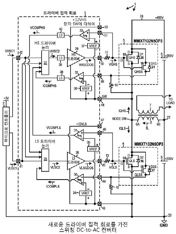
도 2는 하나의 새로운 양태에 따른 새로운 드라이버 집적 회로를 포함하는 스위칭 DC- to-AC 인버터 회로의 도면이다.
도 3은 도 2의 드라이버 집적 회로의 로우 사이드 드라이버 논리 회로의 블록도이다.
도 4는 도 2의 드라이버 집적 회로의 하이 사이드 드라이버 논리 회로의 블록도이다.
도 5는 도 2의 DC- to-AC 인버터 회로의 동작을 도시하는 파형도이다.
도 6은 도 5의 시간 T2과 시간 T6 사이의 시간 주기를 보다 상세히 도시한 단순화된 파형도이다. 파형 다이어그램은 단순화된 것이다. 파형을 보다 정확하게 이해하려면 회로를 제작하고 실제 회로의 실제 신호를 모니터링하고 테스트 장비로 검사해야 한다.
도 7은 하이 사이드 트랜지스터 QHS가 턴 온 되어 하이 사이드 트랜지스터 QHS의 바디 다이오드 D1 주위로 분로 전류(shunt current)를 발생시키고, 바디 다이오드를 통해 흐르는 리버스 리커버리 전류에 의한 손실을 감소시키는 방법(100)의 흐름도이다.
도 8은 로우 사이드 트랜지스터 QLS가 턴 온 되어 로우 사이드 트랜지스터 QLS의 바디 다이오드 D2 주위로 분로 전류(shunt current)를 발생시키고, 바디 다이오드 D2를 통해 흐르는 리버스 리커버리 전류 흐름에 의한 손실을 감소시키는 방법(200)의 흐름도이다.
도 9는 드라이버 집적 회로(3)가 마이크로 컨트롤러로부터 멀티 비트 디지털 제어값을 수신하는 직렬 디지털 인터페이스를 도시하는 도면이며, 멀티 비트 디지털 제어 값은 임계 전압(예를 들어, 임계 전압(62)) 및 임계 전류(예를 들어, 임계 전류(61))를 생성한다.In the accompanying drawings, like reference numerals denote like components and illustrate embodiments of the present invention.
1A (prior art) is a diagram showing the current flow of a DC-to-AC inverter circuit when the low-side transistor is on and in a conduction state.
Fig. 1B (prior art) is a diagram showing a current flow in the DC-to-AC inverter circuit of Fig. 1A when the low-side transistor is turned off.
1C is a diagram showing a current flow in the inverter circuit of FIG. 1A when the low-side transistor is turned on again.
FIG. 1D is a diagram illustrating a current flow of the inverter circuit of FIG. 1A after the reverse recovery current flows in the body diode of the high side transistor.
2 is a diagram of a switching DC-to-AC inverter circuit including a new driver integrated circuit according to one new aspect.
3 is a block diagram of a low-side driver logic circuit of the driver integrated circuit of FIG. 2.
4 is a block diagram of a high side driver logic circuit of the driver integrated circuit of FIG. 2.
5 is a waveform diagram showing the operation of the DC-to-AC inverter circuit of FIG. 2.
6 is a simplified waveform diagram illustrating in more detail a time period between a time T2 and a time T6 of FIG. 5. The waveform diagram is a simplified one. To understand the waveforms more accurately, you need to build the circuit, monitor the real signal in the real circuit, and inspect it with test equipment.
7 shows a method 100 for generating a shunt current around the body diode D1 of the high side transistor QHS when the high side transistor QHS is turned on, and reducing losses due to the reverse recovery current flowing through the body diode. It is a flow chart.
FIG. 8 is a method for generating a shunt current around the body diode D2 of the low-side transistor QLS by turning on the low-side transistor QLS, and reducing the loss due to the reverse recovery current flowing through the body diode D2 (200 ) Is a flow chart.
9 is a diagram showing a serial digital interface through which the driver integrated circuit 3 receives a multi-bit digital control value from a microcontroller, and the multi-bit digital control value is a threshold voltage (for example, a threshold voltage 62) and A threshold current (e.g., threshold current 61) is generated.
이하, 첨부된 도면을 참조하여 본 발명의 실시예를 상세히 설명한다. "디지털 논리 레벨" 및 "디지털 논리값" 이라는 용어는 본 특허 문헌에서 상호 혼용한다.Hereinafter, embodiments of the present invention will be described in detail with reference to the accompanying drawings. The terms "digital logic level" and "digital logic value" are used interchangeably in this patent document.
도 2는 하나의 새로운 양태에 따른 DC-to-AC 인버터 회로 시스템(inverter circuit system)(1)의 도면이다. DC-to-AC 인버터 시스템(1)은 마이크로 컨트롤러 집적 회로(microcontroller integrated circuit)(2), 드라이버 집적 회로(driver integrated circuit)(3), 로우 사이드 트랜지스터(low-side transistor) 소자(device)(4), 하이 사이드 트랜지스터(high-side transistor) 소자(device)(5), 제1 권선(first winding)(6) 및 제2 권선(second winding)(7)을 포함하는 변압기(transformer) , 제1 전압 소스(first voltage source)(8), 제2 전압 소스(second voltage source)(9), 하이 사이드 전류 감지 저항(high-side current sense resistor)(10), 하이 사이드 트랜지스터 소자용 전류 제한 게이트 저항(current limiting gate resistor)(11), 로우 사이드 전류 감지 저항(low-side current sense resistor)(12) 및 로우 사이드 트랜지스터 소자용 전류 제한 게이트 저항(current limiting gate resistor)(13)을 포함한다. 2 is a diagram of a DC-to-AC
로우 사이드 트랜지스터 소자(low-side transistor device)(4) 및 하이 사이드 트랜지스터 소자(high-side transistor device)(5)는 동일한 소자이다. 일례에서, 이들 소자는 캘리포니아주 밀피타스의 버키드라이브 1590의 IXYS사로부터 입수할 수 있는 MMIXT132N5OP3 소자의 사례이다. 로우 사이드 트랜지스터 소자(4)는 로우 사이드 N 채널 전계 효과 트랜지스터(N-channel field effect transistor) QLS(14)와 보다 작은 전류 감지(current sense) N 채널 전계 효과 트랜지스터(N-channel field effect transistor) QLSS(15)를 포함한다.The low-side transistor device 4 and the high-side transistor device 5 are the same device. In one example, these devices are examples of MMIXT132N5OP3 devices available from IXYS of BuckyDrive 1590 of Milpitas, CA. The low-side transistor element (4) includes a low-side N-channel field effect transistor QLS (14) and a smaller current sense N-channel field effect transistor (QLSS). It includes (15).
도면 부호 16은 로우 사이드 트랜지스터(14)의 바디 다이오드(body diode) D2이다. 도면 부호 17은 전류 감지 트랜지스터(current sense transistor)(15)의 바디 다이오드 D2S이다. 트랜지스터(14)와 트랜지스터(15)의 게이트는 함께 연결된다. 트랜지스터(14)와 트랜지스터(15)의 드레인은 함께 연결된다. 전류 감지 트랜지스터(15)는 메인 트랜지스터(main transistor)(14)보다 훨씬 작다. 전류 감지 트랜지스터(15)는 메인 로우 사이드 트랜지스터와 함께 동일한 반도체 다이(die) 상에 제공되어, 전류 감지 트랜지스터(15)를 통한 전류 흐름은 메인 로우 사이드 트랜지스터(14)를 통한 전류 흐름에 비례하게 된다.
하이 사이드 트랜지스터 소자(high-side transistor device)(5)는 하이 사이드 N 채널 전계 효과 트랜지스터(high-side N-channel field effect transistor)(18) 및 보다 작은 전류 감지 N 채널 전계 효과 트랜지스터(current sense N-channel field effect transistor)(19)를 포함한다. 도면 부호 20은 하이 사이드 트랜지스터(high-side transistor)(18)의 바디 다이오드(body diode) D1를 나타낸다. 도면 부호 21은 전류 감지 트랜지스터(current sense transistor)(19)의 바디 다이오드 D1S이다. 트랜지스터(18)와 트랜지스터(19)의 게이트는 함께 연결된다. 트랜지스터(18)와 트랜지스터(19)의 드레인은 함께 연결된다.The high-side transistor device 5 includes a high-side N-channel
제1 전압 소스(8)는 노드(22) 상에 +200 DC 전압을 인가한다. 이 +200 볼트는 접지 노드 GND(23)의 접지 전위를 기준으로 한다. 제1 전압 소스(8)는, 예를 들어 병렬로 결합된 큰 커패시터를 갖는 배터리 또는 다른 전압 소스의 스택(stack)일 수 있다. 제2 전압 소스(9)는 노드(24)에 +200 DC 전압을 제공한다. 이 +200 볼트는 노드(22) 상의 +200 볼트 전위이다. 따라서, 접지 노드 GND(23) 상의 접지 전위에 대하여 노드(24)에는 + 400V DC 전위가 존재한다. 제2 전압 소스(9)는, 예를 들어 병렬로 결합된 큰 커패시터를 갖는 배터리 또는 다른 전압 소스의 스택(stack)일 수 있다.The
하이 사이드 트랜지스터(18)의 드레인은 노드(24)에 연결된다. 하이 사이드 트랜지스터(18)의 소스는 SW 노드(25)에서 로우 사이드 트랜지스터(14)의 드레인에 연결된다. 로우 사이드 트랜지스터(14)의 소스는 접지 노드 GND(23)에 연결된다. 권선(6)의 제1 단부(6A)는 스위칭 노드 SW(25)에 연결되고 그 일부이다. 권선(6)의 제2 단부(6B)는 노드(22)에 연결되고 노드(22)의 일부이다.The drain of the
드라이버 집적 회로(driver integrated circuit)(3)는 로우 사이드 게이트 드라이버 논리 회로(low-side gate driver logic circuit)(26), 하이 사이드 게이트 드라이버 논리 회로(high-side gate driver logic circuit)(27), 로우 사이드 게이트 드라이버 회로(low-side gate driver circuit)(28), 하이 사이드 게이트 드라이버 회로(high-side gate driver circuit)(29), 하이 사이드 전류 감지 비교기(high-side current sense comparator)(32), 하이 사이드 전압 감지 비교기(high-side voltage sense comparator)(33), 로우 사이드 전류 감지 비교기(low-side current sense comparator)(30), 로우 사이드 전압 감지 비교기(low-side voltage sense comparator)(31), 전압 기준 회로(voltage reference circuit)(34 내지 37), 레벨 시프트 회로(level shift circuit)(38 내지 40), VLSC1 로우 사이드 드라이버 디지털 제어 신호 입력 단자(low-side driver digital control signal input terminal)(41), VHSC1 하이 사이드 드라이버 디지털 제어 신호 입력 단자(high-side driver digital control signal input terminal)(42), 접지 단자(ground terminal)(43), 로우 사이드 전류 감지 입력 단자(low-side current sense input terminal)(44), 로우 사이드 드라이버 출력 단자(low-side driver output terminal)(45), 로우 사이드 전압 감지 입력 단자(low-side voltage sense input terminal)(46), 로우 사이드 드라이버 공급 전압 단자(low-side driver supply voltage terminal)(47), SW 노드 단자(SW node terminal)(48), 하이 사이드 전류 감지 입력 단자(high-side current sense input terminal)(49), 하이 사이드 드라이버 출력 단자(high-side driver output terminal)(50), 하이 사이드 전압 감지 입력 단자(high-side voltage sense input terminal)(51) 및 하이 사이드 드라이버 공급 전압 단자(high-side driver supply voltage terminal)(52)을 포함한다. 이들 단자는 드라이버 집적 회로(driver integrated circuit)(3)의 회로 구성을 포함하는 반도체 소자 패키지의 패키지 단자이다. 각각의 패키지 단자에 대해 연관된 집적 회로 다이 터미널(예를 들어, 본드 패드)이 있다. 도 2의 단자 부호는 패키지 단자 및 관련 집적 회로 다이 단자 모두를 나타낸다.The driver integrated circuit (3) includes a low-side gate driver logic circuit (26), a high-side gate driver logic circuit (27), Low-side gate driver circuit (28), high-side gate driver circuit (29), high-side current sense comparator (32) , High-side voltage sense comparator (33), low-side current sense comparator (30), low-side voltage sense comparator (31) ), voltage reference circuit (34 to 37), level shift circuit (38 to 40), VLSC1 low-side driver digital control signal input terminal (41), VHSC1 high-side driver digital control signal input terminal (42), ground terminal (43), low-side current sense input terminal (low-side current sense) input terminal (44), low-side driver output terminal (45), low-side voltage sense input terminal (46), low-side driver output terminal (45), Low-side driver supply voltage terminal (47), SW node terminal (48), high-side current sense input terminal (49), high A high-side driver output terminal 50, a high-side voltage sense input terminal 51, and a high-side driver supply voltage terminal It includes (52). These terminals are package terminals of a semiconductor device package containing the circuit configuration of a driver integrated circuit (3). For each package terminal there is an associated integrated circuit die terminal (eg, bond pad). The terminal symbols in Fig. 2 denote both package terminals and associated integrated circuit die terminals.
동작시, 드라이버 집적 회로(3)는 마이크로 컨트롤러(2)로부터 디지털 로우 사이드 제어 신호 VLSC1를 수신한다. 이 VLSC1 로우 사이드 드라이버 제어 신호가 낮은 디지털 논리 레벨을 가질 때, 마이크로 컨트롤러(2)는 로우 사이드 게이트 드라이버 회로(28)를 제어하여 로우 사이드 트랜지스터 QLS(14)의 게이트 상에 포지티브 전압을 구동하여 로우 사이드 트랜지스터 QLS(14)는 턴 온 되어 전도 상태가 된다. 마찬가지로, 드라이버 집적 회로(3)는 마이크로 컨트롤러(2)로부터 디지털 하이 사이드 제어 신호 VHSC1을 수신한다. 이 VHSC1 제어 신호가 높은 디지털 논리 레벨을 가질 때, 마이크로 컨트롤러(2)는 하이 사이드 트랜지스터 QHS(18)가 턴 온 되어 전도 상태가 되도록 로우 사이드 트랜지스터 QHS(18)의 게이트 상에 포지티브 전압을 구동하도록 하이 사이드 게이트 드라이버 회로(29)를 제어한다.In operation, the driver integrated circuit 3 receives a digital low side control signal VLSC1 from the
마이크로 컨트롤러(2)로부터 수신된 VLSC1 로우 사이드 드라이버 디지털 제어 신호가 낮은 디지털 논리 레벨을 가질 때, 로우 사이드 트랜지스터 QLS(14)가 턴 오프 되고 비전도 상태가 되도록, 항상 드라이버 집적 회로(3)가 로우 사이드 게이트 드라이버 회로(28)을 제어하여 로우 사이드 트랜지스터 QLS(14)의 게이트 상에 낮은 전압을 구동한다고 생각할 수 있으나, 본 발명에 따르면 이것은 항상 사실이 아니다. 아래에서 더 상세히 설명하는 바와 같이, 드라이버 집적 회로(3)는 로우 사이드 트랜지스터(14)의 바디 다이오드(16)를 통해 순방향 전류가 흐르는지를 검출하고, 그리고 이 조건에서, 로우 사이드 트랜지스터 QLS(14)가 턴 온 되도록 로우 사이드 트랜지스터 QLS(14)의 게이트로 높은 전압을 구동한다. 따라서, 마이크로 컨트롤러(2)로부터 수신된 VLSC1 로우 사이드 드라이버 디지털 제어 신호가 낮은 디지털 논리 레벨에 있더라도 로우 사이드 트랜지스터 QLS(14)는 턴 온 된다. 로우 사이드 트랜지스터 QLS(14)가 턴 온 되는 것은 바디 다이오드(16)의 주위에 전류를 분로(shunt) 시키고, 이 시간 동안 바디 다이오드(16) 양단에 발생되었을 전압 강하를 감소시키고, 이로 인하여 바디 다이오드(16)에서 전력 소모를 감소시킨다. 로우 사이드 트랜지스터 QLS(14)는 바디 다이오드(16)가 신속하게 정류(commutate)되는 경우에 역방향 복구 전류의 크기를 감소시키는 역할을 한다. 그러나, 하이 사이드 트랜지스터 QHS(18)가 온 및 전도 상태가 되도록 제어되는 시간 동안, 로우 사이드 트랜지스터 QLS(14)는 턴 온 되지 않고 전도 상태가 되지 않도록 제어된다.When the VLSC1 low side driver digital control signal received from the
유사하게, 마이크로 컨트롤러(2)로부터 수신된 VLHC1 하이 사이드 드라이버 디지털 제어 신호가 낮은 디지털 논리 레벨을 가질 때, 하이 사이드 트랜지스터 QHS(18)가 턴 오프 되고 비전도 상태가 되도록, 항상 드라이버 집적 회로(3)가 하이 사이드 게이트 드라이버 회로(29)을 제어하여 로우 사이드 트랜지스터 QHS(18)의 게이트 상에 낮은 전압을 구동한다고 생각할 수 있으나, 본 발명에 따르면 이것은 항상 사실이 아니다. 아래에서 더 상세히 설명하는 바와 같이, 드라이버 집적 회로(3)는 하이 사이드 트랜지스터(18)의 바디 다이오드(20)를 통해 순방향 전류가 흐르는지를 검출하고, 그리고 이 조건에서, 하이 사이드 트랜지스터 QHS(18)가 턴 온 되도록 하이 사이드 트랜지스터 QHS(18)의 게이트로 높은 전압을 구동한다. 따라서, 마이크로 컨트롤러(2)로부터 수신된 VHSC1 하이 사이드 드라이버 디지털 제어 신호가 낮은 디지털 논리 레벨에 있더라도 하이 사이드 트랜지스터 QHS(18)는 턴 온 된다. 하이 사이드 트랜지스터 QHS(18)가 턴 온 되는 것은, 바디 다이오드(20) 주위의 전류를 분로(shunt) 시키고, 그 시간동안 바디 다이오드(20) 양단에 발생되었을 전압 강하를 감소시키고, 이로 인하여 바디 다이오드(20)의 전력 소모를 감소시킨다. 또한, 바디 다이오드(20)가 신속하게 정류된 다면, 온 상태의 하이 사이드 트랜지스터 QHS(18)는 리버스 리커버리 전류의 크기를 감소시키는 역할을 한다. 그러나, 로우 사이드 트랜지스터 QLS(14)가 온 및 전도 상태가 되도록 제어되는 시간 동안, 하이 사이드 트랜지스터 QHS(18)는 온(on) 되지 않고 전도 상태가 되지 않도록 제어된다.Similarly, when the VLHC1 high side driver digital control signal received from the
도 3은 LS 드라이버 논리(26)의 회로 구성의 일례의 블록도이다. LS 드라이버 논리(LS driver logic)(26)는 지연 회로(delay circuit)(80), 두 개의 강하 에지 검출 회로(falling edge detect circuit)(81 및 82), 상승 에지 검출 회로(rising edge detect circuit)(83), 두 개의 OR 게이트(OR gate)(84 및 85) 및 플립 플롭(flip-flop)(86)을 포함한다. 상승 및 강하 에지 검출 회로는 원샷(one-shot) 회로이다. 3 is a block diagram of an example of the circuit configuration of the
도 4는 HS 드라이버 논리(HS driver logic)(27)의 회로 구성의 일례의 블록도이다. HS 드라이버 논리(27)는 지연 회로(delay circuit)(90), 강하 에지 검출 회로(falling edge detect circuit)(91), 두 개의 상승 에지 검출 회로(rising edge detect circuit)(92 및 93), 두 개의 OR 게이트(94 및 95) 및 플립 플롭(96)을 포함한다. 상승 및 강하 에지 검출 회로는 원샷 회로이다.4 is a block diagram of an example of the circuit configuration of the
도 5는 도 2의 DC-to-AC 인버터 회로의 동작을 도시하는 파형도이다. 상부 파형(55)은 DC-to-AC 인버터 회로가 권선(6)을 통해 구동하는 원하는 정현파 AC 전류 흐름을 나타낸다. 이 권선 전류는 인덕터 전류(inductor current)라고도 하며 IL로 표시된다. 제2 파형 VLSC1(56)은 단자 VLSC1(41)상의 드라이버 집적 회로(3)에 의해 수신된 VLSC1 로우 사이드 드라이버 디지털 제어 신호를 나타낸다. 제3 파형 VHSC1(57)은 단자 VHSC1(42)상의 드라이버 집적 회로(3)에 의해 수신된 VHSC1 디지털 제어 신호를 나타낸다. 하부 파형(58)은 DC-to-AC 인버터 회로가 권선(6)을 통해 구동하는 실제 AC 전류 흐름을 나타낸다. 실제 인덕터 전류(actual inductor current) IL은 완벽한 정현파 파형을 갖지 않지만 정현파 파형에 근사하다. 인덕터 전류 정현파의 첫번째 반주기(half cycle)(59) 동안, VLSC1 로우 사이드 드라이버 제어 신호는 마이크로 컨트롤러(2)에 의해 제어됨으로써 위아래(up and down)로 전이되지만, VHSC1 제어 신호는 디지털 논리의 낮은 레벨로 유지된다. VLSC1 로우 사이드 드라이버 제어 신호가 디지털 논리의 높은 레벨에 있을 때, 하단 파형의 인덕터 전류 IL의 크기가 증가한다는 것에 유의해야 한다. VLSC1 로우 사이드 드라이버 제어 신호가 디지털 논리의 낮은 레벨에 있을 때, 하단 파형의 인덕터 전류 IL의 크기가 떨어지는 것에 유의하자. VLSC1 로우 사이드 드라이버 제어 신호의 펄스의 타이밍 및 듀티 사이클은, 하부 파형(58)에서 결과적인 인덕터 전류가 이상적인 정현파 형상에 근접하도록 하는 것이다.5 is a waveform diagram showing the operation of the DC-to-AC inverter circuit of FIG. 2. The
인덕터 전류 사인파의 두번째 반주기(60) 동안, 마이크로 컨트롤러(2)에 의해 제어될 때 VHSC1 제어 신호는 위아래(up and down)로 전이(transition)하지만, VLSC1 로우 사이드 드라이버 제어 신호는 디지털 논리의 낮은 레벨로 유지된다. VHSC1 제어 신호가 디지털 논리의 높은 레벨에 있을 때, 하부 파형에서의 인덕터 전류 IL의 크기가 떨어지게 되는 것에 유의해야 한다. VHSC1 제어 신호가 디지털 논리의 낮은 레벨에 있을 때, 하부 파형에서의 인덕터 전류 IL의 크기가 상승한다는 것에 유의해야 한다. VHSC1 제어 신호의 펄스의 타이밍 및 듀티 사이클은 결과적인 인덕터 전류 흐름이 원하는 정현파 형태를 갖도록 한다.During the second half cycle (60) of the inductor current sine wave, the VHSC1 control signal transitions up and down when controlled by the
도 6은 시간 T1과 시간 T6 사이의 시간 간격을 보다 상세하게 도시한다. 도 6의 상부 두 개의 파형은 마이크로 컨트롤러(2)로부터 드라이버 집적 회로(3)에 의해 수신된 디지털 제어 신호 VHSC1 및 VLSC1를 나타낸다. 시간 T1에서 시간 T6 사이의 시간 주기가 출력 인덕터 전류(output inductor current) IL의 첫번째 반주기(59) 동안 발생하기 때문에, 마이크로 컨트롤러(2)는 하이 사이드 논리 제어 신호 VHSC1를 디지털 논리의 낮은 레벨로 유지하고 있다. VLSC2로 표기된 네 번째 파형은 로우 사이드 드라이버 회로(26)에 의해 로우 사이드 게이트 드라이버 회로(28)의 입력 리드(input lead) 상에 출력되는 전압 신호이다. 로우 사이드 드라이버 디지털 제어 신호 VLSC1가 시간 T2와 T3 사이의 높은 디지털 논리 레벨에 있을 때, 로우 사이드 게이트 드라이버 회로(28)는 로우 사이드 트랜지스터 QLS(14)의 게이트 상에 12 볼트 VGs 전압을 구동한다. 따라서, 로우 사이드 트랜지스터 QLS(14)는 온 되어 전도 상태가 된다. 따라서, 인덕터 전류 IL은 "인덕터 전류(inductor current) IL"로 표시된 다섯 번째 파형에 도시된 바와 같이 시간 T2와 T3 사이에서 상승한다. 그러나, 시간 T3에서, 마이크로 컨트롤러(2)는 VLSC1 로우 사이드 드라이버 제어 신호가 디지털 논리의 낮은 레벨로 전이되도록 한다. 이러한 강하 에지는 LS 드라이버 논리(26)의 강하 에지 검출기(82)에 의해 검출된다. 강하 에지의 검출은 도 6에서 원으로 둘러싼 "1"로 표시되고 화살표로 나타냈다. 제3 파형에 도시된 펄스는 이 강하 에지 검출기(82)에 의해 출력된 신호 FED82를 도시한다. 이러한 검출 결과로서, 로우 사이드 드라이버 논리(26)은 디지털 논리의 낮은 신호 VLSC2를 로우 사이드 게이트 드라이버 회로(28)에 출력한다. 이어서, 로우 사이드 게이트 드라이버 회로(28)는 로우 사이드 트랜지스터 QLS(14)상의 게이트 전압 VGs를 0 볼트로 낮춘다. 이것은 도 6에서 원으로 둘러싼 "2"로 표시되고 화살표로 나타냈다. 로우 사이드 트랜지스터 QLS(14)의 게이트 전압이 낮음으로 구동되면, 로우 사이드 트랜지스터 QLS(14)는 오프로 된다. 이것은 도 6에서 원으로 둘러싼 "3"으로 표시되고 화살표로 나타냈다. 여섯 번째 파형으로 표시된 로우 사이드 트랜지스터 QLS를 통해 흐르는 전류 IQLS는 0으로 떨어진다. 그러나, 변압기 권선(6)의 큰 인덕턴스를 통해 흐르는 전류 IL은 즉시 정지할 수 없기 때문에, 전류 IL는 SW 노드(25)로부터 하이 사이드 트랜지스터 소자(5)쪽으로 상향 전환된다. 이때 하이 사이드 트랜지스터 QHS(18)는 오프 되어 바디 다이오드 D1(20)을 통해 전류가 노드(24)로 흐른다. SW 노드(25)에서 하이 사이드 트랜지스터 소자(5)로 흐르는 전류 IQHS의 이러한 갑작스러운 증가는 도 6에서 원으로 둘러싼 "4"로 표시되고 화살표로 나타냈다. 시간 T3에서의 전류 상승은 IQHS라고 표기되어 설명된다. 이 전류 IQHS가 소정의 임계 전류(61)를 초과하면, 비교기(32)는 디지털 논리의 높은 신호를 출력한다. 레벨 시프트 회로(38)에 의해 레벨 시프트된 이 신호는 ICOMPHS이다. 신호 ICOMPHS의 상승 에지는 하이 사이드 드라이버 논리(27)의 상승 에지 검출기(93)에 의해 검출된다. 이것은 도 6에서 원으로 둘러싼 "5"로 표시되고 화살표로 나타냈다. 상승 에지 검출기(93)는 신호 ICOMPHS의 상승 에지를 검출하고, 신호 RED93의 하이 펄스를 출력한다. 신호 RED93는 플립 플롭(96)의 설정된 입력 리드 상에 공급되므로, 하이 사이드 드라이버 논리(27)의 플립 플롭(96)이 설정되고, 하이 사이드 드라이버 논리 회로(27)는 그의 출력 신호 VHSC2를 높은 디지털 논리 레벨로 활성(assert)한다. 이것은 도 6에서 원으로 둘러싼 "6"으로 표시되고 화살표로 나타냈다. 다음으로 하이 사이드 게이트 드라이버 회로(29)는 하이 사이드 트랜지스터 QHS(18)의 게이트 상에 12 볼트 게이트 전압 VGs를 구동한다. 이것은 도 6에서 원으로 둘러싼 "7"로 표시되고 화살표로 나타냈다. 하이 사이드 트랜지스터(18)의 게이트 상의 12V의 VGs 전압(SW 노드의 전압에 대한)은 하이 사이드 트랜지스터 QHS(18)를 턴 온 시킨다. 이것은 도 6에서 원으로 둘러싼 "8"로 표시되고 화살표로 나타냈다. IQHS(NFET) 파형에 의해 표시된 바와 같이, 하이 사이드 트랜지스터 QHS(18)는 전류를 전도한다. 이 전류는 IQHS(DIODE)라고 표시된 하단 파형에 나와있는 것처럼 바디 다이오드 D1(20)을 통해 흐르는 전류의 크기는 감소한다. 전류 IQHS(NFET)가 증가할 때, 전류 IQHS(DIODE)는 대응하는 방식으로 감소한다. 단자(42) 상에 입력되는 디지털 제어 신호 VHSC1가 디지털 논리의 낮은 레벨에 있더라도, 하이 사이드 트랜지스터 QHS(18)는 온 되어 전도 상태가 되도록 제어된다.6 shows in more detail the time interval between time T1 and time T6. The upper two waveforms in FIG. 6 represent digital control signals VHSC1 and VLSC1 received by the driver integrated circuit 3 from the
이 상태는 마이크로 컨트롤러(2)가 시간 T4에서 로우 사이드 드라이버 디지털 제어 신호 VLSC1을 디지털 논리의 높은 레벨로 활성(assert)할 때까지 지속된다. 드라이버 집적 회로(3)는 로우 사이드 드라이버 디지털 제어 신호 VLSC1의 상승 에지를 검출하나, 로우 사이드 트랜지스터 QLS(14)를 즉시 제어하지 않는다. 오히려, 먼저 하이 사이드 트랜지스터 QHS(18)를 오프로 제어한다. 우선, 하이 사이드 드라이버 논리(27)의 상승 에지 검출기(92)는 VLSC1 로우 사이드 드라이버 제어 신호의 상승 에지를 검출한다. 이것은 도 6에서 원으로 둘러싼 "9"로 표시되고 화살표로 나타냈다. 도 6의 일곱 번째 파형 RED92에 도시된 펄스는 이 상승 에지 검출기(92)에 의해 출력된 펄스를 나타낸다. 이에 응답하여, 하이 사이드 드라이버 논리(27)는 VHSC2 제어 신호를 디지털 논리의 낮은 레벨로 강제한다. 이것은 도 6에서 원으로 둘러싼 "10"으로 표시되고 화살표로 나타냈다. 이것은 하이 사이드 트랜지스터(18)의 게이트 상의 전압을 감소시킨다. 이것은 도 6에서 원으로 둘러싼 "11"로 표시되고 화살표로 나타냈다. 하이 사이드 트랜지스터(18)의 게이트 상의 전압 신호 VGHS는 레지스터(11)의 저항 및 하이 사이드 트랜지스터 소자(5)의 게이트-소스 커패시턴스에 의해 결정되는 비율로 감소한다. 저항(11) 및 하이 사이드 트랜지스터의 게이트 캐패시턴스 때문에, 단자(50) 상의 신호 VHSGDOS의 전압은 하이 사이드 트랜지스터 QHS(18)의 게이트 상의 신호 VGHS의 전압과 동일하지 않다. 하이 사이드 트랜지스터 QHS(18)의 게이트 상의 신호 VGHS의 전압이 감소함에 따라, 하이 사이드 트랜지스터 QHS(18)를 통한 전류 흐름이 감소한다. 이것은 도 6에서 원으로 표시된 "12"로 표시되고 화살표로 나타냈다. 하이 사이드 트랜지스터 QHS(18)의 게이트 상의 전압 VGHS이 소정의 임계 전압(62) 아래로 떨어지면, 비교기(33)는 그 출력 신호를 디지털 논리의 높은 레벨로 활성 한다. 레벨 시프트 후에, 이 신호는 디지털 신호 VCOMPHS이다. 디지털 신호 VCOMPHS의 이러한 낮음에서 높음으로의 신호 천이는 플립 플롭(86)이 디지털 하이 값으로 클럭 되도록 한다. 따라서, 제어 신호 VLSC2는 디지털 논리값의 높음으로 전이한다. 이것은 도 6에서 원으로 둘러싼 "13"로 표시되고 화살표로 나타냈다. 이는 로우 사이드 트랜지스터 QLS(14)를 턴 온 시키고, 인덕터 전류 IL이 SW 노드(25)로부터 로우 사이드 트랜지스터 QLS(14)를 통하여 접지 노드 GND(23)로 흐르도록 아래쪽으로 리다이렉트(redirect) 되도록 한다. 이것은 도 6에서 원으로 둘러싼 "14"로 표시되고 화살표로 나타냈다. 시간 T5에서 시간 T6까지, 로우 사이드 트랜지스터 QLS(14)를 통과하는 전류 흐름은 도 6에서 IQLS로 표시된 파형에 의해 도시된 바와 같이 증가한다. This state persists until the
따라서, 첫번째 반주기(59) 동안 로우 사이드 트랜지스터 QLS(14)가 먼저 턴 오프 제어되면, 하이 사이드 트랜지스터의 바디 다이오드 D1(20)를 통한 전류의 급격한 증가가 검출된다. 이 검출은 하이 사이드 트랜지스터 QHS(18)를 턴 온 시키기 위한 트리거로서 사용된다. 그렇지 않으면 바디 다이오드 D1(20)을 통과할 전류는 하이 사이드 트랜지스터 QHS(18)를 통과한다. 이렇게 하면 바디 다이오드 D1(20)에서 발생하는 전력 손실을 줄일 수 있다. 하이 사이드 트랜지스터 QHS(18)는 드라이버 집적 회로(3)가 마이크로 컨트롤러(2)로부터의 VLSC1 로우 사이드 드라이버 디지털 제어 신호의 상승 에지를 수신할 때까지 계속해서 온(on) 및 전도 상태가 되도록 제어된다. 마이크로 컨트롤러(2)로부터 수신된 VLSC1 로우 사이드 드라이버 디지털 제어 신호의 상승 에지에 응답하여, 드라이버 집적 회로(3)는 우선 하이 사이드 트랜지스터 QHS(18)를 턴 오프 하도록 제어한다. 하이 사이드 트랜지스터 QHS(18)의 게이트-소스간 전압이 임계 전압 아래로 떨어지면, 드라이버 집적 회로(3)는 슛 스루(shoot-through) 문제를 야기하지 않고 로우 사이드 트랜지스터 QLS(14)를 턴 온 시킬 수 있다. 따라서, 하이 사이드 트랜지스터 QHS(18) 상의 VGs 게이트 전압이 임계 전압 아래로 떨어짐을 검출한 것에 응답하여, 드라이버 집적 회로(3)는 로우 사이드 트랜지스터 QLS(14)를 온으로 제어한다. 그 후, 마이크로 컨트롤러(2)로부터 수신된 VLSC1 로우 사이드 드라이버 디지털 제어 신호가 디지털 논리의 높은 값이 계속 지속된다면, 로우 사이드 트랜지스터 QLS(14)는 온 상태를 유지하고 전도 상태를 유지하도록 제어된다.Accordingly, when the low-
도 7은 도 6의 파형도에 기술된 방법(100)의 흐름도이다. 이 방법(100)은 정현파 AC 출력 전류 IL의 첫번째 반주기(59) 동안 드라이버 집적 회로(3)의 동작에 관한 것이다. 도 6의 시간 T3와 같은 시간에서, 시작에서 로우 사이드 트랜지스터 QLS(14)는 온 된다. VHSC1 하이 사이드 드라이버 디지털 제어 신호는 디지털 논리의 낮은 레벨에 있고 도 7의 방법(100)을 통해 이 레벨로 유지된다. 마이크로 컨트롤러(2)는 로우 사이드 드라이버 제어 신호 VLSC1를 디지털 논리의 낮은 레벨로 비활성 된다. 이로 인해, 로우 사이드 트랜지스터 QLS(14)가 턴 오프 되고, 인덕터 전류 IL의 흐름이 SW 노드(25)로부터 하이 사이드 트랜지스터 소자(5)로 상향 리다이렉트 된다. 따라서 현재 IQHS가 증가한다. 전류 IQHS가 임계 전류를 초과하도록 비교기(32)에 의해 검출되면(단계 101), 드라이버 집적 회로(3)는 하이 사이드 트랜지스터 QHS(18)를 온으로 제어한다(단계 102). 도 2의 예에서, 이러한 검출은 감지 바디 다이오드 D1S(21)를 통한 전류 흐름이 임계 전류를 초과하는지를 검출함으로써 간접적으로 수행된다. 마이크로 컨트롤러(2)가 VHSC1 신호를 디지털 논리의 낮은 레벨로 유지하더라도, 하이 사이드 트랜지스터 QHS는 드라이버 집적 회로(3)에 의해 온으로 제어되고 있다. 마이크로 컨트롤러(2)가 로우 사이드 트랜지스터 QLS(14)를 계속해서 제어하여 오프로 지속하는 한, 드라이버 집적 회로(3)는 하이 사이드 트랜지스터 QHS(18)를 제어하여 계속적으로 턴 온 되어 전도 상태를 유지한다. 이것은 바디 다이오드 D1(20)의 주변으로 전류 흐름을 분로 시키게 된다. 이 분로(shunt) 전류는 하이 사이드 트랜지스터 QHS를 통해 흐른다. 마이크로 컨트롤러(2)가 VLSC1 로우 사이드 드라이버 디지털 제어 신호를 디지털 논리의 높은 레벨로 활성 시켜 로우 사이드 트랜지스터 QLS(14)를 턴 온 하면(단계 103), 드라이버 집적 회로(3)는 우선 하이 사이드 트랜지스터 QHS(18)를 오프로 제어한다(단계 104). 하이 사이드 트랜지스터 QHS(18)의 게이트 상의 전압 VGs이 비교기(33)에 의해 임계 전압 아래로 떨어지는 것으로 검출되면(단계 105), 드라이버 집적 회로(3)는 단자(45) 상에 "로우 사이드 게이트 드라이버 출력 신호"(VLSGDOS)를 활성 한다. 이로 인해, 로우 사이드 트랜지스터 QLS14가 턴 온 된다(단계 106). 마이크로 컨트롤러(2)가 계속하여 VLSC1 로우 사이드 드라이버 제어 신호를 디지털 논리의 높은 레벨로 활성 하는 한, 드라이버 집적 회로(3)는 하이 게이트-소스 전압 신호 VGLS를 로우 사이드 트랜지스터 QLS(14)의 게이트로 계속해서 구동한다. 마이크로 컨트롤러(2)가 VLSC1 로우 사이드 드라이버 제어 신호를 디지털 논리의 낮은 레벨로 비활성 할 때(단계 107), 드라이버 집적 회로(3)는 로우 사이드 트랜지스터 QLS(14)를 오프로 제어하고(단계 108), 단계 101 내지 단계 108을 반복한다. 7 is a flow diagram of the method 100 described in the waveform diagram of FIG. 6. This method 100 relates to the operation of the driver integrated circuit 3 during the
도 5의 첫번째 반주기(59) 동안 전력 손실을 감소시키는 것에 더하여, 드라이버 집적 회로(3)는 도 5의 두번째 반주기(60) 동안 손실을 감소시키기 위해 유사한 방식으로 동작한다. 두번째 반주기(60) 동안, 마이크로 컨트롤러(2)는 고정된 디지털 논리의 낮은 레벨에서 VLSC1 로우 사이드 드라이버 디지털 제어 신호를 유지한다. 그러나, 마이크로 컨트롤러(2)는 인덕터 전류 IL가 도 5에 도시된 정현파 형상을 갖도록 VHSC1 디지털 제어 신호를 펄스(pulse)화 한다. 이 두번째 반주기(60) 동안, 하이 사이드 트랜지스터 QHS(18)는 마이크로 컨트롤러(2)의 제어에서 턴 온 되어 권선(6)을 통해 전류 IL를 푸시(push) 한다. 그러한 전류 펄스는 도 2에서 IL로 표시된 화살표의 방향과 반대 방향이기 때문에, 전류 펄스는 음(negative)의 IL 전류로 간주된다. 따라서, 도 5의 두번째 반주기(60)에서 나타나는 IL 파형은 인덕터 전류 IL가 음(negative)의 값을 포함한다. 하이 사이드 트랜지스터 QHS(18)를 통해 흐르는 이러한 음의 IL 전류의 펄스 이후에, 하이 사이드 트랜지스터 QHS(18)는 턴 오프 된다. 이로 인해 음 전류의 흐름이 리다이렉트(redirect)된다. 그것은 접지 노드 GND(23)로부터 로우 사이드 트랜지스터 QLS(14)의 바디 다이오드 D2(16)를 통해 SW 노드(25)로, 그리고 트랜스포머의 권선(6)을 통해 노드(22)로 흐르도록 리다이렉트(redirect) 된다. 하나의 새로운 양태에서, 드라이버 집적 회로(3)는 이 시간 동안 로우 사이드 트랜지스터 QLS(14)를 턴 온 하도록 제어한다. 따라서 바디 다이오드 D2(16)를 통해 흐르는 전류의 일부는 전도 상태의 로우 사이드 트랜지스터 QLS(14)를 통해 흐른다. 그 다음, 마이크로 컨트롤러(2)가 VHSC1 디지털 제어 신호를 활성하여 하이 사이드 트랜지스터 QHS(18)를 턴 온 시키면, 드라이버 집적 회로(3)는 12 볼트 VGs 신호를 하이 사이드 트랜지스터 QHS(18)의 게이트 상으로 즉시 구동하지 않고, 오히려 로우 사이드 드라이버 논리(26)은 먼저 로우 사이드 트랜지스터 QLS(14)를 턴 오프 시킨다. 드라이버 집적 회로(3)는 하부 사이드 트랜지스터 QLS(14)의 게이트 상의 게이트 전압 신호 VGLS(VGs)를 모니터링 한다. 로우 사이드 트랜지스터 QLS(14)의 게이트 상의 게이트 전압 VGs가 임계 전압(62) 아래로 떨어지는 것이 검출되면, 하이 사이드 드라이버 논리(27)는 하이 사이드 트랜지스터 QHS(18)를 온으로 제어한다. In addition to reducing the power loss during the
도 7의 흐름도는 마이크로 컨트롤러(2)가 VHSC1 신호를 디지털 논리의 낮음으로 유지하는 조건에 대한 것이다. 마이크로 컨트롤러(2)가 VHSC1 신호를 디지털 논리를 높음으로 활성하면, 낮음에서 높음의 전이는 하이 사이드 드라이버 논리(27)의 지연 소자(90)를 통과하고, OR 게이트(95)를 통과하여 플립 플롭(96)을 클럭 한다. 디지털 "1"이 플립 플롭(96)의 D 입력 상에 존재하기 때문에, 플립 플롭(96)은 디지털 논리의 높은 레벨로 클럭 하며, VHSC2 신호는 디지털 논리의 높은 레벨로 활성 될 것이다. 이것은 하이 사이드 드라이버(29)를 통과하여 드라이버 집적 회로(3)로부터 빠져나와 하이 사이드 트랜지스터 QHS를 턴 온 시킬 것이다. 앞에서 설명한 바와 같이, 로우 사이드 트랜지스터 QLS가 드라이버 집적 회로(3)에 의해 온으로 제어되는 경우(VLSC1이 낮음에도 불구하고 바디 다이오드 D2 주위로 전류를 분로 하기 위하여), 하이 사이드 트랜지스터 QHS의 턴 온에서의 지연은 로우 사이드 트랜지스터 QLS가 턴 오프 될 시간을 제공한다. 일 실시예에서, 드라이버 집적 회로(3)는 로우 사이드 트랜지스터 QLS 상의 VGs가 임계 전압 아래이면 하이 사이드 트랜지스터 QHS가 턴 온 되도록 한다.The flowchart of Fig. 7 is for the condition that the
도 8은 마이크로 컨트롤러가 하이 사이드 트랜지스터를 온 및 오프 스위칭 하지만 VLSC1을 낮음으로 유지하는 조건에서, 드라이버 집적 회로(3)의 동작 방법(200)의 흐름도이다. 초기에, 마이크로 컨트롤러(2)는 하이 사이드 트랜지스터 QHS(18)가 온 및 전도 상태가 되도록 제어한다. VLSC1 로우 사이드 드라이버 디지털 제어 신호는 디지털 논리의 낮은 레벨에 있고, 도 8의 방법(200)을 통해 이 레벨로 유지된다. 마이크로 컨트롤러(2)는 디지털 제어 신호 VHSC1를 디지털 논리의 낮은 레벨로 비활성 한다. 이에 응답하여, 드라이버 집적 회로(3)는 하이 사이드 트랜지스터 QHS(18)를 오프로 제어한다. 하이 사이드 트랜지스터 QHS(18)의 턴 오프는 인덕터 전류 IL의 흐름이 리다이렉트 되도록 한다. 인덕터 전류의 흐름은 접지 노드 GND(23)로부터 로우 사이드 트랜지스터 QLS(14)의 바디 다이오드 D1(16)를 통해 SW 노드(25)로, 그리고 나서 권선(6)을 통해 노드(22)로 흐른다. 이 전류 흐름은 IQLS 전류의 화살표와 반대이므로 이 전류 흐름은 음의 IQLC 전류로 간주된다. 비교기(30)에 의해 전류 IQLS가 임계 전류를 초과한 것으로 검출되면(단계 201), 드라이버 집적 회로(3)는 로우 사이드 트랜지스터 QLS(14)를 온으로 제어한다(단계 202). 도 2의 예에서, 이러한 검출은 감지 트랜지스터의 바디 다이오드 D2S(17)를 통한 전류 흐름이 비례 임계 전류(proportionate threshold current)를 초과하는지를 검출함으로써 간접적으로 수행된다. 마이크로 컨트롤러(2)가 하이 사이드 트랜지스터 QHS(18)를 계속해서 제어하여 오프로 지속하는 한, 드라이버 집적 회로(3)는 로우 사이드 트랜지스터 QLS(14)를 계속 제어하여 턴 온 되어 전도 상태를 유지한다. 이것은 바디 다이오드 D2(16) 주위의 전류 흐름을 분로(shunt)시킨다. 마이크로 컨트롤러(2)가 하이 사이드 트랜지스터 QHS(18)를 턴 온 하기 위해 VHSC1 하이 사이드 드라이버 디지털 제어 신호를 디지털 논리의 높은 레벨로 활성 하면(단계 203), 드라이버 집적 회로(3)는 먼저 로우 사이드 트랜지스터 QLS(14)를 오프로 제어한다(단계 204). 드라이버 집적 회로(3)는 비교기(31)에 의해 로우 사이드 트랜지스터 QLS(14)의 게이트 상의 전압 신호 VGLS(VGs)가 임계 전압 아래로 떨어지는 것을 검출하면(단계 205), "하이 사이드 게이트 드라이버 출력 신호 "(VHSGDOS)를 단자(50)에 출력한다. 이는 하이 사이드 트랜지스터 QHS(18)를 턴 온 시킨다(단계 206). 마이크로 컨트롤러(2)가 VHSC1 하이 사이드 드라이버 디지털 제어 신호를 디지털 논리의 높은 레벨로 계속 활성화하는 한, 드라이버 집적 회로(3)는 12 볼트의 게이트-소스 전압 VGs를 하이 사이드 트랜지스터 QHS(18)의 게이트 상으로 계속해서 구동한다. 마이크로 컨트롤러(2)가 VHSC1 하이 사이드 드라이버 디지털 제어 신호를 디지털 논리의 로우 레벨로 비활성화 할 때, 드라이버 집적 회로(3)는 하이 사이드 트랜지스터 QHS(18)를 오프로 제어하고(단계 208), 단계 201 내지 단계 208을 반복한다.8 is a flow chart of a
도 8의 흐름도는 마이크로 컨트롤러(2)가 VLSC1 신호를 디지털 논리를 낮음으로 유지하는 조건에 대한 것이다. 마이크로 컨트롤러(2)가 VLSC1 신호를 디지털 논리를 높음으로 활성 하면, 낮음에서 높음으로의 전이는 로우 사이드 드라이버 논리(26)의 지연 소자(80)를 통과하여 OR 게이트(84)를 통과하여 플립 플롭(86)을 클럭한다. 디지털 "1"이 플립 플롭(86)의 D 입력 상에 존재하기 때문에, 플립 플롭(86)은 디지털 논리 하이 레벨로 클럭하며, VLSC2 신호는 디지털 논리의 높은 레벨로 활성 될 것이다. 이것은 로우 사이드 드라이버(28)를 통과하여 드라이버 집적 회로(3)를 빠져나가서 로우 사이드 트랜지스터 QLS를 턴 온 시킨다. 앞에서 설명한 바와 같이, 하이 사이드 트랜지스터 QHS가 드라이버 집적 회로(3)에 의해 온으로 제어되는 경우(VHSC1이 낮음에도 불구하고 바디 다이오드 D1 주위로 전류를 분로 하기 위하여), 로우 사이드 트랜지스터 QLS의 턴 온에서의 지연은 하이 사이드 트랜지스터 QHS가 턴 오프 될 시간을 제공한다. 일 실시예에서, 드라이버 집적 회로(3)는 하이 사이드 트랜지스터 QHS 상의 VGs가 임계 전압 아래이면 로우 사이드 트랜지스터 QLS가 턴 온 되도록 한다.The flowchart of Fig. 8 is for the condition that the
마이크로 컨트롤러는 감지된 전류와 감지된 전압을 포함하여 다양한 센서 입력을 기반으로 복잡한 방식으로 하이 사이드 드라이버와 로우 사이드 드라이버를 제어할 수 있다. 따라서, 클럭 디지털 마이크로 컨트롤러가 새로운 드라이버 집적 회로(3)의 기능을 수행할 수 있다고 생각할 수 있다. 그러나, 이것은 일반적으로 그렇지 않다. 일 실시예에서, 게이트 드라이버 집적 회로(3)의 하이 및 로우 사이드 드라이버를 제어하는 마이크로 컨트롤러는 비교적 느린 클럭 속도로 클럭 된다. 마이크로 컨트롤러(3)의 비교적 느린 클럭은 여러 가지 이유로 바람직하다. 따라서, 마이크로 컨트롤러(3)는 필요한 전류 및/또는 전압 검출을 할 수 없고, 그러한 검출에 기초하여 결정을 내릴 수 없으며, 원하는 만큼 빠르게 하이 및 로우 사이드 드라이버를 제어함으로써 응답할 수 없다. 따라서, 새로운 게이트 드라이버 집적 회로(3)는 비교기(30 내지 33) 및 관련 회로 구성을 포함하여, 아날로그 영역에서 드라이버 집적 회로(3)가 보다 신속하게 검출하고 응답할 수 있게 한다. 도 6에 화살표 "1" 내지 "8" 및 화살표 "9" 내지 "14"로 표시된 신호 전파는 디지털 클럭 신호의 클럭 에지를 기다릴 필요가 있기 때문에 느려지지 않는다. 게이트 드라이버 집적 회로(3)는 명령들을 패치(fetch)하고 실행하는 어떠한 클럭 디지털 프로세서(clocked digital processor)도 포함하지 않는다.Microcontrollers can control high-side and low-side drivers in a complex manner based on a variety of sensor inputs, including sensed current and sensed voltage. Therefore, it can be considered that the clock digital microcontroller can perform the function of the new driver integrated circuit 3. However, this is generally not the case. In one embodiment, the microcontroller controlling the high and low side drivers of the gate driver integrated circuit 3 is clocked at a relatively slow clock rate. A relatively slow clock of the microcontroller 3 is desirable for several reasons. Thus, the microcontroller 3 is unable to detect the required current and/or voltage, cannot make decisions based on such detection, and cannot respond by controlling the high and low side drivers as quickly as desired. Thus, the new gate driver integrated circuit 3 includes comparators 30 to 33 and associated circuit configurations, allowing the driver integrated circuit 3 to detect and respond more quickly in the analog domain. The signal propagation indicated by arrows "1" to "8" and arrows "9" to "14" in Fig. 6 is not slowed down because it is necessary to wait for the clock edge of the digital clock signal. The gate driver integrated circuit 3 does not contain any clocked digital processor to fetch and execute instructions.
도 9는 도 2의 드라이버 집적 회로(3)의 디지털 인터페이스 논리(63) 및 관련 단자(64 및 65)를 도시한다. 단자(64 및 65) 및 디지털 인터페이스 논리(63)는 도 2의 단순화된 도면에 도시되지 않았다. 디지털 인터페이스 논리(63)는 마이크로 컨트롤러(2)로부터 네 개의 멀티 비트 디지털 제어 레지스터 및 네 개의 대응하는 디지털-아날로그 컨버터(DAC)를 수신하기 위한 I2C 인터페이스를 포함한다. 전압 기준 회로들(34 내지 37) 각각은 이들 다중 비트 제어 레지스터들 및 그 관련 DAC 중 하나이다. 레지스터에 저장된 다중 비트 디지털 제어 값은 DAC에 공급되어 DAC가 원하는 기준 전압을 출력한다. 마이크로 컨트롤러(2)는 단자 SDA(64) 및 단자 SCL(65)에 직렬로 디지털 신호를 공급함으로써, 네 개의 제어 레지스터 각각에 멀티 비트 디지털 전압 제어 값을 기입하고, 전압 기준 회로(34 내지 37)에 의해 출력되는 각각의 기준 전압을 제어 및 설정한다. 도체(68)는 비교기(33)의 반전(inverting) 입력 리드(lead)에 연결된다. 도체(69)는 비교기(32)의 비반전(non-inverting) 입력 리드에 연결된다. 도체(70)는 비교기(31)의 비반전 입력 리드에 연결된다. 도체(71)는 비교기(30)의 비반전 입력 리드에 연결된다. 수직 점선(72)은 도 2의 드라이버 집적 회로(3)의 좌측 경계를 나타낸다. 따라서, 전압 기준 회로(34 내지 37)에 의해 출력된 기준 전압은 마이크로 컨트롤러(2)에 의해 프로그램 가능하다.9 shows the
특정의 구체적인 실시예가 교시 목적을 위해 상기 설명되었지만, 본 특허 문헌의 교시는 일반적인 적용 가능성을 가지며 앞에서 설명한 특정 실시예에 한정되지 않는다. 이 새로운 게이트 드라이버는 가장 유리하게 마이크로 컨트롤러와 별 개인 집적 회로 상에 배치되지만, 또한 새로운 게이트 드라이버는 마이크로 컨트롤러와 함께 동일한 집적 회로 상에 배치될 수 있다. 따라서, 청구 범위에서 설명된 본 발명의 범위를 벗어나지 않고 설명된 실시예들의 다양한 특징의 다양한 변형, 개조 및 조합이 실시될 수 있다.Although certain specific embodiments have been described above for teaching purposes, the teachings of this patent document have general applicability and are not limited to the specific embodiments described above. This new gate driver is most advantageously placed on an integrated circuit separate from the microcontroller, but also the new gate driver can be placed on the same integrated circuit with the microcontroller. Accordingly, various modifications, adaptations, and combinations of various features of the described embodiments may be implemented without departing from the scope of the invention described in the claims.
Claims (24)
(a) 하이 사이드 드라이버 디지털 제어 신호 - 상기 하이 사이드 드라이버 디지털 제어 신호는 제1 디지털 논리값을 가짐 - 를 수신하는 단계;
(b) (a)단계의 제1 디지털 논리값의 하이 사이드 드라이버 디지털 제어 신호의 수신에 응답하여, 상기 하이 사이드 트랜지스터가 오프로 제어되도록 하이 사이드 트랜지스터의 게이트 상에 하이 사이드(HS) 게이트 신호를 구동하는 단계;
(c) 상기 다이오드를 통과하는 전류의 흐름이 상승하여 임계 전류를 초과하는 것으로 결정하는 - 상기 하이 사이드 드라이버 디지털 제어 신호가 상기 제1 디지털 논리값에 있을 때 (c)단계의 결정이 발생됨 - 단계;
(d) (c)단계의 결정에 응답하여, 상기 하이 사이드 트랜지스터가 온 되도록 상기 하이 사이드 트랜지스터의 게이트 상에 상기 하이 사이드(HS) 게이트 신호를 구동하는 단계;
(e) 상기 로우 사이드 드라이버 디지털 제어 신호 - 상기 로우 사이드 드라이버 디지털 제어 신호는 상기 제1 디지털 논리값을 가짐 - 를 수신하는 단계;
(f) 상기 로우 사이드 드라이버 디지털 제어 신호가 상기 제1 디지털 논리값으로부터 제2 디지털 논리값으로의 전이 - (c)단계의 결정 이후 (f)단계에서 상기 로우 사이드 드라이버 디지털 제어 신호는 상기 제1 디지털 논리값으로부터 상기 제2 디지털 논리값으로 전이됨 - 를 검출하는 단계;
(g) (f)단계의 검출에 응답하여, 상기 하이 사이드 트랜지스터가 오프 되도록 상기 하이 사이드 트랜지스터의 게이트 상에 상기 하이 사이드(HS) 게이트 신호를 구동하는 단계;
(h) 상기 하이 사이드 트랜지스터의 게이트-소스 전압이 임계 전압 아래로 강하 - (g)단계의 상기 하이 사이드(HS) 게이트 신호의 구동에 응답하여 (h)단계에서 상기 하이 사이드 트랜지스터의 게이트-소스 전압이 임계 전압 이하로 강하됨 - 되는지를 결정하는 단계;
(i) (h)단계의 결정에 응답하여, 상기 로우 사이드 트랜지스터가 제어되어 턴 온 되도록 로우 사이드 트랜지스터의 게이트 상에 로우 사이드(LS) 게이트 신호를 구동하는 단계; 및
(j) 상기 로우 사이드 드라이버 디지털 제어 신호가 상기 제2 디지털 논리값으로 유지되는 동안 - 상기 하이 사이드 드라이버 디지털 제어 신호는 상기 제1 디지털 논리값으로 유지되고, (c)단계 내지 (j)단계 중 임의의 시간에서 제2 디지털 논리값으로 디지털 값을 전이하지 않음 -, 상기 로우 사이드 트랜지스터가 온 상태를 유지하도록 상기 로우 사이드 트랜지스터의 게이트 상에 상기 로우 사이드(LS) 게이트 신호를 구동하는 단계;
를 포함하는 방법
A method comprising a high side transistor and a low side transistor, wherein a source of the high side transistor is connected to a drain of the low side transistor, and a diode is disposed in parallel with the high side transistor,
(a) receiving a high side driver digital control signal, the high side driver digital control signal having a first digital logic value;
(b) In response to receiving the high side driver digital control signal of the first digital logic value in step (a), a high side (HS) gate signal is applied on the gate of the high side transistor so that the high side transistor is controlled to be off. Driving;
(c) determining that the flow of current through the diode rises to exceed a threshold current-the determination of step (c) occurs when the high-side driver digital control signal is at the first digital logic value-step ;
(d) driving the high-side (HS) gate signal on the gate of the high-side transistor to turn on the high-side transistor in response to the determination in step (c);
(e) receiving the low side driver digital control signal, the low side driver digital control signal having the first digital logic value;
(f) transition of the low-side driver digital control signal from the first digital logic value to a second digital logic value-After the determination in step (c), in step (f), the low-side driver digital control signal is Detecting a transition from a digital logic value to the second digital logic value;
(g) driving the high-side (HS) gate signal on the gate of the high-side transistor so that the high-side transistor is turned off in response to the detection in step (f);
(h) the gate-source voltage of the high-side transistor falls below a threshold voltage-in response to the driving of the high-side (HS) gate signal in step (g), the gate-source of the high-side transistor in step (h) Determining whether the voltage drops below a threshold voltage;
(i) driving a low-side (LS) gate signal on the gate of the low-side transistor so that the low-side transistor is controlled and turned on in response to the determination in step (h); And
(j) while the low side driver digital control signal is maintained at the second digital logic value-the high side driver digital control signal is maintained at the first digital logic value, and during steps (c) to (j) Not transitioning a digital value to a second digital logic value at any time-driving the low side (LS) gate signal on the gate of the low side transistor to keep the low side transistor on;
How to include
상기 하이 사이드 트랜지스터는 N 채널 전계 효과 트랜지스터이고,
상기 다이오드는 상기 N 채널 전계 효과 트랜지스터의 바디 다이오드인
방법.
The method of claim 1,
The high side transistor is an N-channel field effect transistor,
The diode is a body diode of the N-channel field effect transistor
Way.
상기 하이 사이드 트랜지스터는 전류 감지 트랜지스터와 함께 반도체 다이 상에 배치되고,
상기 전류 감지 트랜지스터는 바디 다이오드를 가지며,
상기 하이 사이드 트랜지스터의 게이트는 상기 전류 감지 트랜지스터의 게이트에 연결되고,
상기 하이 사이드 트랜지스터의 드레인은 상기 전류 감지 트랜지스터의 드레인에 연결되고,
(c)단계의 결정하는 단계는,
상기 전류 감지 트랜지스터가 오프로 제어되는 시간 동안,
상기 전류 감지 트랜지스터의 바디 다이오드를 통한 전류 흐름을 검출하는
단계를 포함하는
방법.
The method of claim 2,
The high side transistor is disposed on the semiconductor die together with the current sensing transistor,
The current sensing transistor has a body diode,
A gate of the high side transistor is connected to a gate of the current sensing transistor,
A drain of the high side transistor is connected to a drain of the current sensing transistor,
The determining step of step (c) is:
During the time when the current sensing transistor is controlled to be off,
Detecting the current flow through the body diode of the current sensing transistor
Including steps
Way.
(c)단계의 결정하는 단계는,
제2 전류 - 상기 제2 전류는 상기 다이오드를 통과하는 전류 흐름을 나타냄 - 가 임계 전류를 초과하는지를
결정하는 단계를 포함하는
방법.
The method of claim 1,
The determining step of step (c) is:
Whether the second current-the second current represents the current flow through the diode-exceeds a threshold current
Including determining
Way.
상기 (a)단계 내지 (j)단계는 게이트 드라이버 집적 회로에 의해 수행되고,
상기 게이트 드라이버 집적 회로는 명령을 패치하여 실행하는 어떠한 디지털 프로세서를 포함하지 않고,
상기 하이 사이드 드라이버 디지털 제어 신호는 (a)단계에서 상기 게이트 드라이버 집적 회로의 제1 패키지 단자 상에 수신되고,
상기 로우 사이드 드라이버 디지털 제어 신호는 (e)단계에서 상기 게이트 드라이버 집적 회로의 제2 패키지 단자 상에 수신되는
방법.
The method of claim 1,
Steps (a) to (j) are performed by a gate driver integrated circuit,
The gate driver integrated circuit does not include any digital processor that fetches and executes instructions,
The high-side driver digital control signal is received on the first package terminal of the gate driver integrated circuit in step (a),
The low side driver digital control signal is received on the second package terminal of the gate driver integrated circuit in step (e).
Way.
Priority Applications (1)
| Application Number | Priority Date | Filing Date | Title |
|---|---|---|---|
| KR1020200178730A KR102467987B1 (en) | 2018-02-21 | 2020-12-18 | Gate driver for switching converter having body diode power loss minimization |
Applications Claiming Priority (2)
| Application Number | Priority Date | Filing Date | Title |
|---|---|---|---|
| US15/901,829 | 2018-02-21 | ||
| US15/901,829 US10090751B1 (en) | 2018-02-21 | 2018-02-21 | Gate driver for switching converter having body diode power loss minimization |
Related Child Applications (1)
| Application Number | Title | Priority Date | Filing Date |
|---|---|---|---|
| KR1020200178730A Division KR102467987B1 (en) | 2018-02-21 | 2020-12-18 | Gate driver for switching converter having body diode power loss minimization |
Publications (2)
| Publication Number | Publication Date |
|---|---|
| KR20190100861A KR20190100861A (en) | 2019-08-29 |
| KR102195552B1 true KR102195552B1 (en) | 2020-12-28 |
Family
ID=63638772
Family Applications (2)
| Application Number | Title | Priority Date | Filing Date |
|---|---|---|---|
| KR1020190017372A Active KR102195552B1 (en) | 2018-02-21 | 2019-02-14 | Gate driver for switching converter having body diode power loss minimization |
| KR1020200178730A Active KR102467987B1 (en) | 2018-02-21 | 2020-12-18 | Gate driver for switching converter having body diode power loss minimization |
Family Applications After (1)
| Application Number | Title | Priority Date | Filing Date |
|---|---|---|---|
| KR1020200178730A Active KR102467987B1 (en) | 2018-02-21 | 2020-12-18 | Gate driver for switching converter having body diode power loss minimization |
Country Status (6)
| Country | Link |
|---|---|
| US (2) | US10090751B1 (en) |
| EP (2) | EP4057509B1 (en) |
| JP (2) | JP6855522B2 (en) |
| KR (2) | KR102195552B1 (en) |
| CN (2) | CN113315403B (en) |
| TW (2) | TWI709293B (en) |
Families Citing this family (21)
| Publication number | Priority date | Publication date | Assignee | Title |
|---|---|---|---|---|
| CN111769730B (en) * | 2016-07-13 | 2024-09-24 | 富士电机株式会社 | Power Module |
| US10090751B1 (en) * | 2018-02-21 | 2018-10-02 | Ixys, Llc | Gate driver for switching converter having body diode power loss minimization |
| DE102018220247A1 (en) * | 2018-11-26 | 2020-05-28 | Robert Bosch Gmbh | Circuit breaker arrangement |
| US10862483B2 (en) * | 2019-01-25 | 2020-12-08 | Infineon Technologies Austria Ag | Low power cycle to cycle bit transfer in gate drivers |
| CN110138367B (en) * | 2019-05-16 | 2020-12-08 | 东南大学 | Gate Drive Circuit for Reducing Reverse Recovery Current of Power Devices |
| US11183835B2 (en) * | 2019-07-16 | 2021-11-23 | Infineon Technologies Austria Ag | Short circuit detection and protection for a gate driver circuit and methods of detecting the same using logic analysis |
| US10855183B1 (en) * | 2019-07-24 | 2020-12-01 | Infineon Technologies Ag | Method and device to operate a power switch in multiple modes |
| CN110557106B (en) * | 2019-08-14 | 2023-09-05 | 成都芯源系统有限公司 | Switch unit turn-off protection circuit and protection method |
| US10958268B1 (en) * | 2019-09-04 | 2021-03-23 | Infineon Technologies Austria Ag | Transformer-based driver for power switches |
| EP3958466B1 (en) | 2020-08-18 | 2024-05-15 | Aptiv Technologies AG | Triggering circuit and electronic fuse device incorporating the same |
| US11264985B1 (en) * | 2021-03-04 | 2022-03-01 | Aes Global Holdings Pte Ltd. | Bipolar pulsed-voltage gate driver |
| CN113544621B (en) * | 2021-06-07 | 2024-04-12 | 长江存储科技有限责任公司 | Power leakage blocking in low drop-out regulators |
| KR102526974B1 (en) * | 2021-07-21 | 2023-04-27 | 비테스코 테크놀로지스 게엠베하 | Apparatus for controlling pn relay for vehicle |
| US11552633B1 (en) * | 2021-10-15 | 2023-01-10 | Stmicroelectronics S.R.L. | Driver circuit with enhanced control for current and voltage slew rates |
| CN114123737A (en) * | 2021-11-03 | 2022-03-01 | 哈尔滨工业大学(深圳) | System and method for reducing power loss of MOSFET (metal-oxide-semiconductor field effect transistor) |
| US12087355B2 (en) * | 2021-12-17 | 2024-09-10 | Mediatek Inc. | Adaptive control circuit of static random access memory |
| TWI788245B (en) | 2022-01-19 | 2022-12-21 | 立錡科技股份有限公司 | Pulse width modulation controller and control method thereof |
| TWI796199B (en) * | 2022-02-21 | 2023-03-11 | 立錡科技股份有限公司 | Power converter and control method thereof |
| US12040692B2 (en) * | 2022-06-02 | 2024-07-16 | Murata Manufacturing Co., Ltd. | Circuits and methods for generating a continuous current sense signal |
| US20250260341A1 (en) * | 2024-02-13 | 2025-08-14 | Hamilton Sundstrand Corporation | Bi-directional power converter utilizing mosfet switching elements |
| GB2641777A (en) * | 2024-06-12 | 2025-12-17 | Dyson Technology Ltd | A gate driver |
Citations (4)
| Publication number | Priority date | Publication date | Assignee | Title |
|---|---|---|---|---|
| US20120043950A1 (en) * | 2010-08-18 | 2012-02-23 | Truong Tom C | System and method for controlling a power switch in a power supply system |
| US20120062190A1 (en) | 2010-09-10 | 2012-03-15 | Holger Haiplik | Dc-dc converters |
| JP2013143804A (en) | 2012-01-10 | 2013-07-22 | Denso Corp | Driving device for switching element |
| JP2016167978A (en) | 2016-05-17 | 2016-09-15 | 三菱電機株式会社 | Synchronous rectifier circuit |
Family Cites Families (23)
| Publication number | Priority date | Publication date | Assignee | Title |
|---|---|---|---|---|
| US6759692B1 (en) * | 2002-02-04 | 2004-07-06 | Ixys Corporation | Gate driver with level shift circuit |
| GB0227792D0 (en) * | 2002-11-29 | 2003-01-08 | Koninkl Philips Electronics Nv | Driver for switching circuit and drive method |
| JP4046752B2 (en) * | 2006-05-09 | 2008-02-13 | シャープ株式会社 | POWER CIRCUIT DEVICE AND ELECTRONIC DEVICE HAVING THE POWER CIRCUIT DEVICE |
| JP4735429B2 (en) * | 2006-06-09 | 2011-07-27 | 株式会社デンソー | Load drive device |
| US9118259B2 (en) * | 2007-12-03 | 2015-08-25 | Texas Instruments Incorporated | Phase-shifted dual-bridge DC/DC converter with wide-range ZVS and zero circulating current |
| JP2011015461A (en) * | 2009-06-30 | 2011-01-20 | Shindengen Electric Mfg Co Ltd | Signal control circuit |
| US7986172B2 (en) * | 2009-08-31 | 2011-07-26 | Freescale Semiconductor, Inc. | Switching circuit with gate driver having precharge period and method therefor |
| DE102010013353A1 (en) * | 2010-03-30 | 2011-10-06 | Texas Instruments Deutschland Gmbh | Switching converter control circuit |
| EP2815491A2 (en) * | 2012-05-24 | 2014-12-24 | Siemens Aktiengesellschaft | Gate driver for a power converter |
| JP5812027B2 (en) * | 2013-03-05 | 2015-11-11 | 株式会社デンソー | Drive control device |
| US9696350B2 (en) * | 2013-03-15 | 2017-07-04 | Intel Corporation | Non-linear control for voltage regulator |
| CN107888056B (en) * | 2013-07-10 | 2020-04-17 | 株式会社电装 | Drive control device |
| JP5939281B2 (en) * | 2013-07-10 | 2016-06-22 | 株式会社デンソー | Drive control device |
| JP6277691B2 (en) * | 2013-11-28 | 2018-02-14 | 株式会社オートネットワーク技術研究所 | Control signal generation circuit and circuit device |
| JP6221930B2 (en) * | 2014-05-13 | 2017-11-01 | 株式会社デンソー | Switching element drive circuit |
| US9543940B2 (en) * | 2014-07-03 | 2017-01-10 | Transphorm Inc. | Switching circuits having ferrite beads |
| US9960620B2 (en) * | 2014-09-16 | 2018-05-01 | Navitas Semiconductor, Inc. | Bootstrap capacitor charging circuit for GaN devices |
| CN107112895B (en) * | 2015-01-12 | 2020-04-17 | 曹华 | Switching regulator and control method thereof |
| JP6337803B2 (en) * | 2015-03-03 | 2018-06-06 | 株式会社デンソー | Synchronous rectifier circuit |
| JP2017005974A (en) * | 2015-06-04 | 2017-01-05 | 株式会社デンソー | Synchronous rectification circuit |
| JP6591220B2 (en) * | 2015-07-15 | 2019-10-16 | ルネサスエレクトロニクス株式会社 | Semiconductor device and power control device |
| US9813055B2 (en) * | 2016-04-01 | 2017-11-07 | Ixys Corporation | Gate driver that drives with a sequence of gate resistances |
| US10090751B1 (en) * | 2018-02-21 | 2018-10-02 | Ixys, Llc | Gate driver for switching converter having body diode power loss minimization |
-
2018
- 2018-02-21 US US15/901,829 patent/US10090751B1/en active Active
- 2018-10-02 US US16/149,745 patent/US10439483B2/en active Active
-
2019
- 2019-02-14 KR KR1020190017372A patent/KR102195552B1/en active Active
- 2019-02-18 EP EP22170847.2A patent/EP4057509B1/en active Active
- 2019-02-18 EP EP19157722.0A patent/EP3570440B1/en active Active
- 2019-02-20 TW TW108105515A patent/TWI709293B/en active
- 2019-02-20 TW TW109133185A patent/TWI748662B/en active
- 2019-02-21 CN CN202110584433.6A patent/CN113315403B/en active Active
- 2019-02-21 JP JP2019029200A patent/JP6855522B2/en not_active Expired - Fee Related
- 2019-02-21 CN CN201910131053.XA patent/CN110176871B/en active Active
-
2020
- 2020-12-18 KR KR1020200178730A patent/KR102467987B1/en active Active
-
2021
- 2021-03-17 JP JP2021043530A patent/JP7039744B2/en not_active Expired - Fee Related
Patent Citations (4)
| Publication number | Priority date | Publication date | Assignee | Title |
|---|---|---|---|---|
| US20120043950A1 (en) * | 2010-08-18 | 2012-02-23 | Truong Tom C | System and method for controlling a power switch in a power supply system |
| US20120062190A1 (en) | 2010-09-10 | 2012-03-15 | Holger Haiplik | Dc-dc converters |
| JP2013143804A (en) | 2012-01-10 | 2013-07-22 | Denso Corp | Driving device for switching element |
| JP2016167978A (en) | 2016-05-17 | 2016-09-15 | 三菱電機株式会社 | Synchronous rectifier circuit |
Also Published As
| Publication number | Publication date |
|---|---|
| TWI709293B (en) | 2020-11-01 |
| US10090751B1 (en) | 2018-10-02 |
| JP2022001009A (en) | 2022-01-04 |
| EP4057509A1 (en) | 2022-09-14 |
| US20190260281A1 (en) | 2019-08-22 |
| CN113315403B (en) | 2024-05-17 |
| CN110176871A (en) | 2019-08-27 |
| US10439483B2 (en) | 2019-10-08 |
| CN110176871B (en) | 2021-06-11 |
| JP7039744B2 (en) | 2022-03-22 |
| JP6855522B2 (en) | 2021-04-07 |
| TW202118208A (en) | 2021-05-01 |
| JP2019180228A (en) | 2019-10-17 |
| EP4057509B1 (en) | 2024-06-26 |
| KR102467987B1 (en) | 2022-11-17 |
| EP3570440A1 (en) | 2019-11-20 |
| TWI748662B (en) | 2021-12-01 |
| KR20200145797A (en) | 2020-12-30 |
| TW201937837A (en) | 2019-09-16 |
| CN113315403A (en) | 2021-08-27 |
| KR20190100861A (en) | 2019-08-29 |
| EP3570440B1 (en) | 2022-06-08 |
Similar Documents
| Publication | Publication Date | Title |
|---|---|---|
| KR102195552B1 (en) | Gate driver for switching converter having body diode power loss minimization | |
| US9537400B2 (en) | Switching converter with dead time between switching of switches | |
| US7345896B2 (en) | Secondary side power supply controller and method therefor | |
| US6396250B1 (en) | Control method to reduce body diode conduction and reverse recovery losses | |
| CN110165872B (en) | Switch control circuit and control method thereof | |
| CN107276574A (en) | Circuit and power converter for soft turn-off of power switches | |
| EP2157682A1 (en) | Switching power supply device and primary side control circuit | |
| EP3557744B1 (en) | A synchronous rectification circuit, corresponding device and method | |
| US10218258B1 (en) | Apparatus and method for driving a power stage | |
| US10734908B2 (en) | Synchronous rectifier control | |
| US8681514B2 (en) | Controller for secondary side control of a switch, power converter, and related synchronous rectification control method | |
| US9391501B2 (en) | VCC charge and free-wheeling detection via source controlled MOS transistor | |
| US11056969B2 (en) | Boost converter short circuit protection | |
| US10523118B2 (en) | Reverse recovery charge elimination in DC/DC power converters | |
| EP3993264A1 (en) | Switch controller, device and method with overcurrent protection | |
| CN121689756A (en) | Intelligent multi-stage power driving |
Legal Events
| Date | Code | Title | Description |
|---|---|---|---|
| A201 | Request for examination | ||
| PA0109 | Patent application |
St.27 status event code: A-0-1-A10-A12-nap-PA0109 |
|
| PA0201 | Request for examination |
St.27 status event code: A-1-2-D10-D11-exm-PA0201 |
|
| PG1501 | Laying open of application |
St.27 status event code: A-1-1-Q10-Q12-nap-PG1501 |
|
| D13-X000 | Search requested |
St.27 status event code: A-1-2-D10-D13-srh-X000 |
|
| D14-X000 | Search report completed |
St.27 status event code: A-1-2-D10-D14-srh-X000 |
|
| E902 | Notification of reason for refusal | ||
| PE0902 | Notice of grounds for rejection |
St.27 status event code: A-1-2-D10-D21-exm-PE0902 |
|
| E13-X000 | Pre-grant limitation requested |
St.27 status event code: A-2-3-E10-E13-lim-X000 |
|
| P11-X000 | Amendment of application requested |
St.27 status event code: A-2-2-P10-P11-nap-X000 |
|
| P13-X000 | Application amended |
St.27 status event code: A-2-2-P10-P13-nap-X000 |
|
| E701 | Decision to grant or registration of patent right | ||
| PE0701 | Decision of registration |
St.27 status event code: A-1-2-D10-D22-exm-PE0701 |
|
| A107 | Divisional application of patent | ||
| PA0107 | Divisional application |
St.27 status event code: A-0-1-A10-A18-div-PA0107 St.27 status event code: A-0-1-A10-A16-div-PA0107 |
|
| GRNT | Written decision to grant | ||
| PR0701 | Registration of establishment |
St.27 status event code: A-2-4-F10-F11-exm-PR0701 |
|
| PR1002 | Payment of registration fee |
St.27 status event code: A-2-2-U10-U11-oth-PR1002 Fee payment year number: 1 |
|
| PG1601 | Publication of registration |
St.27 status event code: A-4-4-Q10-Q13-nap-PG1601 |
|
| PR1001 | Payment of annual fee |
St.27 status event code: A-4-4-U10-U11-oth-PR1001 Fee payment year number: 4 |
|
| PR1001 | Payment of annual fee |
St.27 status event code: A-4-4-U10-U11-oth-PR1001 Fee payment year number: 5 |
|
| PR1001 | Payment of annual fee |
St.27 status event code: A-4-4-U10-U11-oth-PR1001 Fee payment year number: 6 |
|
| U11 | Full renewal or maintenance fee paid |
Free format text: ST27 STATUS EVENT CODE: A-4-4-U10-U11-OTH-PR1001 (AS PROVIDED BY THE NATIONAL OFFICE) Year of fee payment: 6 |