KR100728852B1 - Semiconductor device - Google Patents
Semiconductor device Download PDFInfo
- Publication number
- KR100728852B1 KR100728852B1 KR1020050042307A KR20050042307A KR100728852B1 KR 100728852 B1 KR100728852 B1 KR 100728852B1 KR 1020050042307 A KR1020050042307 A KR 1020050042307A KR 20050042307 A KR20050042307 A KR 20050042307A KR 100728852 B1 KR100728852 B1 KR 100728852B1
- Authority
- KR
- South Korea
- Prior art keywords
- wiring
- metal ion
- semiconductor device
- ion binder
- resin
- Prior art date
- Legal status (The legal status is an assumption and is not a legal conclusion. Google has not performed a legal analysis and makes no representation as to the accuracy of the status listed.)
- Expired - Lifetime
Links
Images


Classifications
-
- H—ELECTRICITY
- H10—SEMICONDUCTOR DEVICES; ELECTRIC SOLID-STATE DEVICES NOT OTHERWISE PROVIDED FOR
- H10W—GENERIC PACKAGES, INTERCONNECTIONS, CONNECTORS OR OTHER CONSTRUCTIONAL DETAILS OF DEVICES COVERED BY CLASS H10
- H10W70/00—Package substrates; Interposers; Redistribution layers [RDL]
- H10W70/60—Insulating or insulated package substrates; Interposers; Redistribution layers
- H10W70/67—Insulating or insulated package substrates; Interposers; Redistribution layers characterised by their insulating layers or insulating parts
- H10W70/69—Insulating materials thereof
-
- H—ELECTRICITY
- H10—SEMICONDUCTOR DEVICES; ELECTRIC SOLID-STATE DEVICES NOT OTHERWISE PROVIDED FOR
- H10W—GENERIC PACKAGES, INTERCONNECTIONS, CONNECTORS OR OTHER CONSTRUCTIONAL DETAILS OF DEVICES COVERED BY CLASS H10
- H10W74/00—Encapsulations, e.g. protective coatings
-
- H—ELECTRICITY
- H05—ELECTRIC TECHNIQUES NOT OTHERWISE PROVIDED FOR
- H05K—PRINTED CIRCUITS; CASINGS OR CONSTRUCTIONAL DETAILS OF ELECTRIC APPARATUS; MANUFACTURE OF ASSEMBLAGES OF ELECTRICAL COMPONENTS
- H05K3/00—Apparatus or processes for manufacturing printed circuits
- H05K3/22—Secondary treatment of printed circuits
- H05K3/28—Applying non-metallic protective coatings
- H05K3/285—Permanent coating compositions
-
- H—ELECTRICITY
- H05—ELECTRIC TECHNIQUES NOT OTHERWISE PROVIDED FOR
- H05K—PRINTED CIRCUITS; CASINGS OR CONSTRUCTIONAL DETAILS OF ELECTRIC APPARATUS; MANUFACTURE OF ASSEMBLAGES OF ELECTRICAL COMPONENTS
- H05K3/00—Apparatus or processes for manufacturing printed circuits
- H05K3/30—Assembling printed circuits with electric components, e.g. with resistors
- H05K3/303—Assembling printed circuits with electric components, e.g. with resistors with surface mounted components
- H05K3/305—Affixing by adhesive
-
- H—ELECTRICITY
- H10—SEMICONDUCTOR DEVICES; ELECTRIC SOLID-STATE DEVICES NOT OTHERWISE PROVIDED FOR
- H10W—GENERIC PACKAGES, INTERCONNECTIONS, CONNECTORS OR OTHER CONSTRUCTIONAL DETAILS OF DEVICES COVERED BY CLASS H10
- H10W70/00—Package substrates; Interposers; Redistribution layers [RDL]
- H10W70/60—Insulating or insulated package substrates; Interposers; Redistribution layers
- H10W70/62—Insulating or insulated package substrates; Interposers; Redistribution layers characterised by their interconnections
- H10W70/66—Conductive materials thereof
- H10W70/666—Organic materials or pastes
-
- H—ELECTRICITY
- H10—SEMICONDUCTOR DEVICES; ELECTRIC SOLID-STATE DEVICES NOT OTHERWISE PROVIDED FOR
- H10W—GENERIC PACKAGES, INTERCONNECTIONS, CONNECTORS OR OTHER CONSTRUCTIONAL DETAILS OF DEVICES COVERED BY CLASS H10
- H10W70/00—Package substrates; Interposers; Redistribution layers [RDL]
- H10W70/60—Insulating or insulated package substrates; Interposers; Redistribution layers
- H10W70/67—Insulating or insulated package substrates; Interposers; Redistribution layers characterised by their insulating layers or insulating parts
- H10W70/688—Flexible insulating substrates
-
- H—ELECTRICITY
- H10—SEMICONDUCTOR DEVICES; ELECTRIC SOLID-STATE DEVICES NOT OTHERWISE PROVIDED FOR
- H10W—GENERIC PACKAGES, INTERCONNECTIONS, CONNECTORS OR OTHER CONSTRUCTIONAL DETAILS OF DEVICES COVERED BY CLASS H10
- H10W70/00—Package substrates; Interposers; Redistribution layers [RDL]
- H10W70/60—Insulating or insulated package substrates; Interposers; Redistribution layers
- H10W70/67—Insulating or insulated package substrates; Interposers; Redistribution layers characterised by their insulating layers or insulating parts
- H10W70/69—Insulating materials thereof
- H10W70/695—Organic materials
-
- H—ELECTRICITY
- H10—SEMICONDUCTOR DEVICES; ELECTRIC SOLID-STATE DEVICES NOT OTHERWISE PROVIDED FOR
- H10W—GENERIC PACKAGES, INTERCONNECTIONS, CONNECTORS OR OTHER CONSTRUCTIONAL DETAILS OF DEVICES COVERED BY CLASS H10
- H10W74/00—Encapsulations, e.g. protective coatings
- H10W74/01—Manufacture or treatment
- H10W74/012—Manufacture or treatment of encapsulations on active surfaces of flip-chip devices, e.g. forming underfills
-
- H—ELECTRICITY
- H10—SEMICONDUCTOR DEVICES; ELECTRIC SOLID-STATE DEVICES NOT OTHERWISE PROVIDED FOR
- H10W—GENERIC PACKAGES, INTERCONNECTIONS, CONNECTORS OR OTHER CONSTRUCTIONAL DETAILS OF DEVICES COVERED BY CLASS H10
- H10W74/00—Encapsulations, e.g. protective coatings
- H10W74/10—Encapsulations, e.g. protective coatings characterised by their shape or disposition
- H10W74/15—Encapsulations, e.g. protective coatings characterised by their shape or disposition on active surfaces of flip-chip devices, e.g. underfills
-
- H—ELECTRICITY
- H05—ELECTRIC TECHNIQUES NOT OTHERWISE PROVIDED FOR
- H05K—PRINTED CIRCUITS; CASINGS OR CONSTRUCTIONAL DETAILS OF ELECTRIC APPARATUS; MANUFACTURE OF ASSEMBLAGES OF ELECTRICAL COMPONENTS
- H05K1/00—Printed circuits
- H05K1/02—Details
- H05K1/03—Use of materials for the substrate
- H05K1/0393—Flexible materials
-
- H—ELECTRICITY
- H05—ELECTRIC TECHNIQUES NOT OTHERWISE PROVIDED FOR
- H05K—PRINTED CIRCUITS; CASINGS OR CONSTRUCTIONAL DETAILS OF ELECTRIC APPARATUS; MANUFACTURE OF ASSEMBLAGES OF ELECTRICAL COMPONENTS
- H05K2201/00—Indexing scheme relating to printed circuits covered by H05K1/00
- H05K2201/07—Electric details
- H05K2201/0753—Insulation
- H05K2201/0769—Anti metal-migration, e.g. avoiding tin whisker growth
-
- H—ELECTRICITY
- H05—ELECTRIC TECHNIQUES NOT OTHERWISE PROVIDED FOR
- H05K—PRINTED CIRCUITS; CASINGS OR CONSTRUCTIONAL DETAILS OF ELECTRIC APPARATUS; MANUFACTURE OF ASSEMBLAGES OF ELECTRICAL COMPONENTS
- H05K2201/00—Indexing scheme relating to printed circuits covered by H05K1/00
- H05K2201/10—Details of components or other objects attached to or integrated in a printed circuit board
- H05K2201/10613—Details of electrical connections of non-printed components, e.g. special leads
- H05K2201/10621—Components characterised by their electrical contacts
- H05K2201/10674—Flip chip
-
- H—ELECTRICITY
- H05—ELECTRIC TECHNIQUES NOT OTHERWISE PROVIDED FOR
- H05K—PRINTED CIRCUITS; CASINGS OR CONSTRUCTIONAL DETAILS OF ELECTRIC APPARATUS; MANUFACTURE OF ASSEMBLAGES OF ELECTRICAL COMPONENTS
- H05K2201/00—Indexing scheme relating to printed circuits covered by H05K1/00
- H05K2201/10—Details of components or other objects attached to or integrated in a printed circuit board
- H05K2201/10613—Details of electrical connections of non-printed components, e.g. special leads
- H05K2201/10954—Other details of electrical connections
- H05K2201/10977—Encapsulated connections
-
- H—ELECTRICITY
- H05—ELECTRIC TECHNIQUES NOT OTHERWISE PROVIDED FOR
- H05K—PRINTED CIRCUITS; CASINGS OR CONSTRUCTIONAL DETAILS OF ELECTRIC APPARATUS; MANUFACTURE OF ASSEMBLAGES OF ELECTRICAL COMPONENTS
- H05K2203/00—Indexing scheme relating to apparatus or processes for manufacturing printed circuits covered by H05K3/00
- H05K2203/12—Using specific substances
- H05K2203/122—Organic non-polymeric compounds, e.g. oil, wax or thiol
- H05K2203/124—Heterocyclic organic compounds, e.g. azole, furan
-
- H—ELECTRICITY
- H10—SEMICONDUCTOR DEVICES; ELECTRIC SOLID-STATE DEVICES NOT OTHERWISE PROVIDED FOR
- H10W—GENERIC PACKAGES, INTERCONNECTIONS, CONNECTORS OR OTHER CONSTRUCTIONAL DETAILS OF DEVICES COVERED BY CLASS H10
- H10W72/00—Interconnections or connectors in packages
- H10W72/851—Dispositions of multiple connectors or interconnections
- H10W72/853—On the same surface
- H10W72/856—Bump connectors and die-attach connectors
-
- H—ELECTRICITY
- H10—SEMICONDUCTOR DEVICES; ELECTRIC SOLID-STATE DEVICES NOT OTHERWISE PROVIDED FOR
- H10W—GENERIC PACKAGES, INTERCONNECTIONS, CONNECTORS OR OTHER CONSTRUCTIONAL DETAILS OF DEVICES COVERED BY CLASS H10
- H10W90/00—Package configurations
- H10W90/701—Package configurations characterised by the relative positions of pads or connectors relative to package parts
- H10W90/721—Package configurations characterised by the relative positions of pads or connectors relative to package parts of bump connectors
- H10W90/724—Package configurations characterised by the relative positions of pads or connectors relative to package parts of bump connectors between a chip and a stacked insulating package substrate, interposer or RDL
-
- H—ELECTRICITY
- H10—SEMICONDUCTOR DEVICES; ELECTRIC SOLID-STATE DEVICES NOT OTHERWISE PROVIDED FOR
- H10W—GENERIC PACKAGES, INTERCONNECTIONS, CONNECTORS OR OTHER CONSTRUCTIONAL DETAILS OF DEVICES COVERED BY CLASS H10
- H10W90/00—Package configurations
- H10W90/701—Package configurations characterised by the relative positions of pads or connectors relative to package parts
- H10W90/731—Package configurations characterised by the relative positions of pads or connectors relative to package parts of die-attach connectors
- H10W90/734—Package configurations characterised by the relative positions of pads or connectors relative to package parts of die-attach connectors between a chip and a stacked insulating package substrate, interposer or RDL
-
- Y—GENERAL TAGGING OF NEW TECHNOLOGICAL DEVELOPMENTS; GENERAL TAGGING OF CROSS-SECTIONAL TECHNOLOGIES SPANNING OVER SEVERAL SECTIONS OF THE IPC; TECHNICAL SUBJECTS COVERED BY FORMER USPC CROSS-REFERENCE ART COLLECTIONS [XRACs] AND DIGESTS
- Y02—TECHNOLOGIES OR APPLICATIONS FOR MITIGATION OR ADAPTATION AGAINST CLIMATE CHANGE
- Y02P—CLIMATE CHANGE MITIGATION TECHNOLOGIES IN THE PRODUCTION OR PROCESSING OF GOODS
- Y02P70/00—Climate change mitigation technologies in the production process for final industrial or consumer products
- Y02P70/50—Manufacturing or production processes characterised by the final manufactured product
Landscapes
- Engineering & Computer Science (AREA)
- Manufacturing & Machinery (AREA)
- Microelectronics & Electronic Packaging (AREA)
- Structures Or Materials For Encapsulating Or Coating Semiconductor Devices Or Solid State Devices (AREA)
- Non-Metallic Protective Coatings For Printed Circuits (AREA)
- Wire Bonding (AREA)
Abstract
본 발명의 반도체 장치는 기재에 복수의 배선이 배치된 배선 기판, 배선 기판에 탑재된 반도체 소자, 및 금속 이온 결합제가 혼합된 재료를 포함하는 배선과 접하는 부재, 또는 표면에 금속 이온 결합제가 첨가된 배선을 구비하고 있기 때문에, 배선으로부터의 금속 이온의 석출에 의한 마이그레이션 발생을 방지할 수 있고, 고신뢰성의 반도체 장치를 제공할 수 있다.The semiconductor device of the present invention includes a wiring board having a plurality of wirings disposed on a substrate, a semiconductor element mounted on the wiring board, and a member in contact with a wiring including a material mixed with a metal ion binder, or a metal ion binder added to a surface thereof. Since the wiring is provided, migration occurrence due to precipitation of metal ions from the wiring can be prevented, and a highly reliable semiconductor device can be provided.
반도체 장치, 마이그레이션, 금속 이온 결합제, 가요성 배선 기판Semiconductor Devices, Migration, Metal Ion Binders, Flexible Wiring Boards
Description
도 1(a)는 본 발명의 실시 형태에 따른 반도체 장치를 나타내는 평면도이다.1A is a plan view of a semiconductor device according to an embodiment of the present invention.
도 1(b)는 반도체의 제조 공정에 있어서, 도 1(a)의 반도체 장치가 테이프 캐리어에 탑재되어 있는 상태를 나타내는 도면이다.FIG. 1B is a diagram showing a state in which the semiconductor device of FIG. 1A is mounted on a tape carrier in a semiconductor manufacturing process.
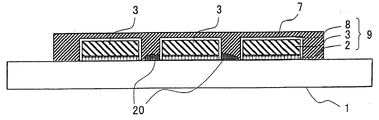
도 2는 도 1(a)의 반도체 장치의 A-A' 단면을 나타내는 단면도이다.FIG. 2 is a cross-sectional view taken along line AA ′ of the semiconductor device of FIG. 1A.
도 3은 도 1(a)의 반도체 장치의 B-B' 단면을 나타내는 단면도이다.3 is a cross-sectional view illustrating a B-B 'cross section of the semiconductor device of FIG. 1A.
도 4는 마이그레이션을 일으킨 반도체 장치를 나타내는 평면도이다.4 is a plan view of the semiconductor device that caused the migration.
도 5(a)는 봉지 수지의 마이그레이션 억제 효과를 측정하기 위한 빗살 모양의 배선 기판을 나타내는 전체의 평면도이다.Fig. 5A is a plan view of the whole of a comb-tooth shaped wiring board for measuring the migration inhibitory effect of the sealing resin.
도 5(b)는 도 5(a)에 있어서의 A 부분을 확대한 도면이다.FIG. 5B is an enlarged view of a portion A in FIG. 5A.
도 6은 도 5(a) 및 도 5(b)의 빗살 모양의 배선이 마이그레이션을 일으킨 경우를 나타내는 평면도이다.FIG. 6 is a plan view showing a case in which the comb-tooth shaped wirings of FIGS. 5A and 5B cause migration.
도 7은 금속 이온 결합제를 포함하는 봉지 수지의 마이그레이션 억제 효과를 나타내는 도면이다.It is a figure which shows the migration inhibitory effect of the sealing resin containing a metal ion binder.
도 8은 반도체 장치에 점도가 높은 봉지 수지를 충전한 경우의 기포를 포함하는 봉지 수지를 나타내는 단면도이다.It is sectional drawing which shows the sealing resin containing the bubble in the case where the semiconductor device is filled with the sealing resin with high viscosity.
도 9는 종래의 반도체 장치의 단면도이다.9 is a cross-sectional view of a conventional semiconductor device.
<도면의 주요 부분에 대한 부호의 간단한 설명><Brief description of symbols for the main parts of the drawings>
1 : 베이스 필름1: base film
2 : 장벽층2: barrier layer
3 : 도전층3: conductive layer
4 : 금 범프4: gold bump
5 : 반도체 칩5: semiconductor chip
6 : 봉지 수지6: resin bag
7 : 솔더 레지스트7: solder resist
8 : 주석 도금8: tin plating
9 : 배선9: wiring
10 : 가요성 배선 기판10: flexible wiring board
11 : 반도체 장치11: semiconductor device
본 발명은 반도체 장치에 관한 것으로, 특히 배선의 마이그레이션을 억제하는 반도체 장치에 관한 것이다.TECHNICAL FIELD This invention relates to a semiconductor device. Specifically, It is related with the semiconductor device which suppresses migration of wiring.
전자 부품을 배선 기판에 탑재한 반도체 장치로서는 가요성 배선 기판 상에 반도체 소자를 접합·탑재한 반도체 장치(COF: Chip On Film), 및 가요성 배선 기판 상에 연속해서 반도체 소자가 접속된 반도체 장치(TCP: Tape Carrier Package) 가 공지되어 있다. COF 및 TCP는 주로 액정 드라이버 IC를 탑재한 반도체 장치에 적용되고 있다.As a semiconductor device in which an electronic component is mounted on a wiring board, a semiconductor device (COF: Chip On Film) in which a semiconductor device is bonded and mounted on a flexible wiring board, and a semiconductor device in which semiconductor devices are continuously connected on a flexible wiring board (TCP: Tape Carrier Package) is known. COF and TCP are mainly applied to semiconductor devices equipped with liquid crystal driver ICs.
최근, 액정 드라이버의 다출력화의 요구에 응하기 위해, 액정 드라이버 IC를 탑재한 가요성 배선 기판의 배선 패턴의 미세 피치화가 급속히 진행되고 있다. 현재로선, TCP에 비해 COF 쪽이 배선 패턴의 미세 피치화에 적절하기 때문에, 액정 드라이버 IC의 포장 형식은 COF가 주류가 되고 있다.In recent years, in order to meet the demand of the multi-output of a liquid crystal driver, the fine pitch of the wiring pattern of the flexible wiring board which mounted the liquid crystal driver IC is progressing rapidly. Currently, since COF is more suitable for finer pitch wiring pattern than TCP, COF has become a mainstream packaging method for liquid crystal driver ICs.
이하에, 종래의 COF의 어셈블리 방법을 도 9를 참조하여 설명한다.Hereinafter, a conventional assembly method of COF will be described with reference to FIG. 9.
처음에 가요성 배선 기판(50)을 제작하는 방법을 나타낸다. 먼저, 폴리이미드 기재(51) 상에 스퍼터법으로 장벽 기능을 갖는 금속층을 형성시키고, 또한 금속화법으로 구리박을 형성시킨다(구리 도금 처리를 행함). 이어서, 구리박 위에 포토레지스트를 도포·경화시키고, 그 이후에 포토레지스트에 패턴 노광시켜 현상하여 목적하는 배선 패턴 형상의 포토레지스트 패턴을 형성한다. 그리고, 포토레지스트 패턴에 따라 구리박 및 장벽 기능을 갖는 금속층을 에칭한 후, 포토레지스트를 박리 처리함으로써 목적하는 패턴 형상을 전사한다. 이에 따라, 배선 패턴 형상의 장벽층(52) 및 구리를 포함하는 도체층(53)이 형성된다. 이어서, 도체 패턴 전면에 균일하게 두께 0.4 내지 0.6 ㎛의 주석 도금(58)을 실시함으로써 배선(59)이 완성된다. 또한, 배선(59)의 보호를 위해, 배선(59) 표면에서의 반도체 칩과의 접속에 관여하지 않는 부분에, 솔더 레지스트(solder resist)(57)를 피복 보호한다. 이에 따라, 가요성 배선 기판(50)이 완성된다.First, the method of manufacturing the
제작된 가요성 배선 기판(50)은 금 범프(54)(돌기 전극)를 형성시킨 반도체 칩과 접합된다. 이 때, 주석 도금(58)과 금 범프(54)를 주석-금 공정(共晶) 접합시킨다. 또한, 상기 접합 공정은 내부 리드 결합(ILB; Inner Lead Bonding)이라 불린다.The produced
ILB 후에, 반도체 칩(55)의 보호를 목적으로, 반도체 칩(55)과 가요성 배선 기판(50)과의 사이에 언더필(underfill)의(즉 경열화성의) 봉지 수지(56)를 충전하고 가열 처리함으로써 봉지 수지를 경화시킨다.After ILB, an underfill (ie, thermosetting)
이후에, 최종적인 전기적 특성 테스트를 실시하여 COF의 어셈블리가 완료된다.Thereafter, the final electrical property test is performed to complete the assembly of the COF.
이러한 반도체 장치에 있어서, 최근에는 한층 더 다출력화가 요구되고 있어, 배선(59)에 걸리는 전압의 고전압화 및 배선 패턴의 미세 피치화가 진행되고 있다. 그러나, 종래의 반도체 장치에서는 이 배선(59)의 고전압화 미세 피치화에 미처 완전하게 대응하지 못해, 배선(59) 간의 마이그레이션이 발생하고 있었다. 마이그레이션은 고습도 하에서 서로 마주 보는 배선에 직류 전압이 인가되었을 때, 전기 화학 반응에 의해 배선 재료의 금속이 이온화되면서 용출되어, 배선의 재료가 본래의 배선 배치 위치가 아닌 장소에 석출되어 성장해 가는 현상이다. 즉, 1개의 배선(59)에 걸리는 전압이 높아지면, 인접하는 배선(59)에 걸리는 전압과의 전위차가 커져 배선(59) 간에 마이그레이션이 발생하기 쉬워지고, 또한 배선(59) 간의 공간이 미세화되면, 배선(59)에 인접하는 배선(59)에 미치는 전계 강도가 강해져 마이그레이션이 발생하기 쉬워지는 것이다.In such a semiconductor device, more output is required in recent years, and a high voltage of the voltage applied to the
마이그레이션이 발생하면, 배선(59)끼리 사이에도 금속 이온이 석출됨으로써 배선(59)의 사이를 단락시켜 절연 파괴에 이르는 현상이 발생하므로, 반도체 장치의 신뢰성이 상실된다. 따라서, 장기간에 걸쳐 마이그레이션의 발생을 억제하는 것이 반도체 장치의 신뢰성을 확보하는데 있어서 중요한 과제가 된다.When migration occurs, a phenomenon occurs that causes metal ions to precipitate between the
마이그레이션의 발생을 억제하는 방법으로는, 첫번째로 고습도가 되는 것을 방지하기 위해서, 배선 사이에 수분이 진입되는 것을 방지하는 방습 수단을 마련하는 것을 생각할 수 있다. 방습 수단으로서는 배선에의 수분의 침입 경로가 되는 가요성 배선 기판의 기재, 솔더 레지스트 및 봉지 수지에 방습성을 부여하는 것을 생각할 수 있다. 그러나, 이러한 부재 중 어떤 것도 투수성이 있는 유기 고분자 재료를 사용할 필요가 있기 때문에, 수분의 진입을 완전하게 차단하는 것은 어렵다. 또한, 방수 도막을 도포하는 방법도 있지만, 번거롭고 비용이 요구되는 방법이고, 마이그레이션 억제의 효과도 불충분하다.As a method of suppressing the occurrence of migration, it is conceivable to provide moisture-proof means for preventing moisture from entering between wirings in order to prevent high humidity from becoming first. As a moisture proof means, it can be considered to provide moisture proof property to the base material, soldering resist, and sealing resin of a flexible wiring board which becomes a penetration path of moisture to wiring. However, since any of these members needs to use a water-permeable organic polymer material, it is difficult to completely block the ingress of moisture. Moreover, although the method of apply | coating a waterproofing coating film is also a troublesome and costly method, the effect of suppression of migration is also inadequate.
두번째로, 배선 재료의 금속 이온의 용출을 가속시키는 염화물 이온 등의 할로겐 이온의 혼입을 줄이는 방법을 생각할 수 있다. 그러나, 할로겐 이온은 사용하는 원재료 자체에 이미 혼입되어 있어, 할로겐 이온 등의 불순물 이온을 완전하게 제거하는 것은 어렵다.Second, a method of reducing the incorporation of halogen ions such as chloride ions which accelerates the elution of metal ions in the wiring material can be considered. However, the halogen ions are already mixed in the raw material itself to be used, and it is difficult to completely remove impurity ions such as halogen ions.
세번째로, 배선에 걸리는 전계 강도를 줄임으로써 배선 재료의 금속 이온의 용해 속도를 감소시키는 방법을 생각할 수 있다. 그러나, 반도체 장치의 고밀도 실장 및 반도체 칩의 고기능화를 달성하기 위해서는, 탑재하는 반도체 칩과 가요성 배선 기판과의 접속 피치의 미세화, 또는 배선에의 인가 전압의 고전압화를 피할 수 없고, 배선 패턴에 걸리는 전계 강도가 강해지는 것도 피할 수 없다.Third, a method of reducing the dissolution rate of metal ions of the wiring material by reducing the electric field strength applied to the wiring can be considered. However, in order to achieve high-density mounting of semiconductor devices and high functionalization of semiconductor chips, miniaturization of the connection pitch between the semiconductor chip to be mounted and the flexible wiring board or high voltage of the applied voltage to the wiring cannot be avoided. Increasing electric field strength is inevitable.
이와 같이, COF의 반도체 장치에서 배선을 미세화, 또는 배선에 고전압을 인가했을 경우에, 비용을 들이지 않고서는 마이그레이션의 발생을 방지하지 못하여 반도체 장치의 고기능화에 방해가 되고 있었다.As described above, in the case of miniaturizing the wiring or applying a high voltage to the wiring in the semiconductor device of the COF, the migration cannot be prevented without incurring costs, which hinders the functionalization of the semiconductor device.
한편, 일본 공개 특허 공보 [특허 공개 평 11-144527(공개일: 1999년 5월 28일)]에는, 전자 부품을 기판에 접착하는 도전 페이스트에서 발생하는 은 이온의 마이그레이션을 막기 위해, 도전 페이스트에 이온화된 은 이온 및 사슬체를 형성하는 은 이온 결합제를 혼합시키는 것이 기재되어 있다. 그러나, 이러한 도전 페이스트는 반도체의 배선에는 적용할 수 없기 때문에 배선의 마이그레이션을 해결할 수는 없다.On the other hand, Japanese Patent Application Laid-Open No. 11-144527 (published date: May 28, 1999) discloses a conductive paste in order to prevent migration of silver ions generated in a conductive paste that adheres electronic components to a substrate. It has been described to mix ionized silver ions and silver ion binders that form chains. However, such a conductive paste cannot be applied to the wiring of the semiconductor, and thus migration of the wiring cannot be solved.
본 발명의 목적은 배선으로부터의 금속 이온의 석출에 의한 마이그레이션 발생을 방지할 수 있는 고신뢰성의 반도체 장치를 제공하는 것이다.An object of the present invention is to provide a highly reliable semiconductor device that can prevent migration from occurring due to precipitation of metal ions from wirings.
상기의 목적을 달성하기 위해, 본 발명의 반도체 장치는, 기재에 복수의 배선이 배치된 배선 기판, 및 상기 배선 기판에 탑재된 반도체 소자를 포함하는 반도체 장치에 있어서, 금속 이온 결합제가 혼합된 재료를 포함하는 배선과 접하는 부재, 또는 표면에 금속 이온 결합제가 첨가된 배선을 구비하는 것을 특징으로 한다.In order to achieve the above object, the semiconductor device of the present invention is a semiconductor device comprising a wiring board on which a plurality of wirings are arranged on a substrate, and a semiconductor element mounted on the wiring board, wherein the metal ion binder is mixed with the material. And a wire in which a metal ion binder is added to the member or the surface in contact with the wire including the wire.
이에 따라, 배선으로부터 방출된 재료의 금속 이온이 배선과 접하는 부재에 포함되거나, 또는 배선 표면에 첨가되는 금속 이온 결합제와 접촉하여 금속 이온을 포착하므로, 금속 이온이 석출되는 것을 방지할 수 있다.Accordingly, the metal ions of the material released from the wiring are contained in the member in contact with the wiring, or the metal ions are trapped in contact with the metal ion binder added to the wiring surface, thereby preventing the deposition of metal ions.
배선으로부터 유출된 금속 이온이 석출되면, 배선으로부터 금속이 성장해 가 고(마이그레이션), 마지막에는 배선에 인접하는 배선과 접속된다. 이 경우, 배선 간의 절연성이 파괴되어 반도체 소자가 양호하게 외부 장치와 접속하지 못하고 동작 불량을 일으킨다.When the metal ions flowing out of the wiring precipitate, the metal grows from the wiring (migrates) and is finally connected to the wiring adjacent to the wiring. In this case, the insulation between the wirings is broken and the semiconductor element can not be connected to the external device satisfactorily and causes malfunction.
본 발명에 의하면, 이러한 배선으로부터의 금속의 석출을 방지할 수 있으므로, 금속의 성장도 방지할 수 있어 반도체 장치가 이러한 동작 불량을 일으키지 않게 된다.According to the present invention, the deposition of metal from such wiring can be prevented, so that the growth of metal can be prevented and the semiconductor device does not cause such a malfunction.
또한, 본 발명의 반도체 장치는 부가적으로 상기 배선 기판과 반도체 소자와의 사이에 적어도 일부가 배선에 접하도록 배치된 봉지 수지를 갖고, 봉지 수지가 금속 이온 결합제를 포함하고 있는 것을 특징으로 한다.In addition, the semiconductor device of the present invention is further characterized by having an encapsulating resin disposed at least partially in contact with the wiring between the wiring board and the semiconductor element, and the encapsulating resin contains a metal ion binder.
여기서, 봉지 수지는 배선 기판, 반도체 소자, 그 접속부의 보호 및 접속의 보강을 위해서 일반적으로 설치되는 것이다.Here, sealing resin is generally provided in order to protect a wiring board, a semiconductor element, its connection part, and reinforcement of a connection.
이에 따르면, 봉지 수지에 금속 이온 결합제가 포함되어 있으므로, 봉지 수지에 포함되는 금속 이온 결합제가 배선에 작용할 수 있다. 즉, 배선으로부터 유출된 금속 이온이 봉지 수지 중의 금속 이온 결합제와 접촉하여 포착되므로, 금속 이온이 봉지 수지 중에 머물러 석출되지 않는다.According to this, since the metal ion binder is contained in the sealing resin, the metal ion binder contained in the sealing resin can act on the wiring. That is, since the metal ions flowing out from the wiring are captured in contact with the metal ion binder in the sealing resin, the metal ions do not remain in the sealing resin and precipitate.
따라서, 종래의 반도체 장치에 있어서 제조 공정 또는 부재의 수를 증가시키는 일 없이, 봉지 수지에 금속 이온 결합제를 첨가하는 것만으로 배선으로부터의 금속 이온의 석출을 방지할 수 있다. 그 결과, 배선으로부터의 금속의 성장이 방지되어 반도체 장치의 동작 불량이 방지된다.Therefore, in the conventional semiconductor device, it is possible to prevent the precipitation of metal ions from the wiring by simply adding a metal ion binder to the sealing resin without increasing the number of manufacturing steps or the number of members. As a result, growth of metal from the wiring is prevented, and a malfunction of the semiconductor device is prevented.
본 발명의 반도체 장치는 상기 봉지 수지가 배선 기판과 반도체 소자와의 사 이에 충전될 때, 점도 50 mPa·s 이상 1250 mPa·s 이하인 것을 특징으로 한다.The semiconductor device of the present invention is characterized by having a viscosity of 50 mPa · s or more and 1250 mPa · s or less when the encapsulation resin is filled between the wiring board and the semiconductor element.
봉지 수지는 경화되기 전의 유동성이 있는 상태로 배선 기판과 반도체 소자와의 사이에 빈틈없이 충전된 후, 경화된다. 따라서, 금속 이온 결합제를 첨가했을 경우에도, 빈틈없이 충전될 수 있는 정도의 유동성을 가지고 있는 것이 바람직하다.The encapsulating resin is hardly filled between the wiring board and the semiconductor element in a state of fluidity before curing, and then cured. Therefore, even when a metal ion binder is added, it is preferable to have fluidity of the grade which can be filled up tightly.
따라서, 봉지 수지의 경화 전, 즉 배선 기판과 반도체 소자와의 사이에 충전될 때에, 점도를 상기 범위로 함으로써 용이하게 도포할 수 있어, 배선 기판과 반도체 소자와의 사이에 빈틈없이 충전될 수 있을 정도의 유동성이 봉지 수지에 구비된다.Therefore, before curing of the encapsulation resin, i.e., when filling between the wiring board and the semiconductor element, the viscosity can be easily applied by making it within the above range, and it can be filled seamlessly between the wiring board and the semiconductor element. The degree of fluidity is provided in the sealing resin.
또한, 점도가 점도 50 mPa·s보다 작으면 유동성이 너무 높아 봉지 수지가 유출되거나, 반도체 소자 측에, 특히 반도체 소자 측면에 부착될 수 없다고 하는 문제가 발생한다. 한편, 점도가 1250 mPa·s보다 크면 유동성이 너무 낮아 분배기로부터 유출되기 어려워 봉지 수지 내에 빈틈이 남을 가능성이 있다.In addition, when the viscosity is smaller than the viscosity of 50 mPa · s, the fluidity is too high, so that the encapsulating resin flows out, or a problem arises in that it cannot be attached to the semiconductor element side, in particular to the semiconductor element side surface. On the other hand, when the viscosity is larger than 1250 mPa · s, the fluidity is too low, so that it is difficult to flow out from the distributor, and there is a possibility that a gap remains in the sealing resin.
또한, 본 발명의 반도체 장치는 상기 봉지 수지가 상기 금속 이온 결합제를 0.5 중량% 이상 10.0 중량% 이하 포함하는 것을 특징으로 한다.Moreover, the semiconductor device of this invention is characterized by the said sealing resin containing 0.5 weight% or more and 10.0 weight% or less of the said metal ion binder.
이에 따르면, 경화 전 상태로 용이하게 도포할 수 있고 배선 기판과 반도체 소자와의 사이에 빈틈없이 충전될 수 있는 정도의 유동성을 갖춤과 동시에, 금속 이온 결합제에 의한 충분한 마이그레이션 억제 효과도 갖는다.According to this, it has the fluidity | liquidity which can be apply | coated easily in the state before hardening, and can be filled seamlessly between a wiring board and a semiconductor element, and also has sufficient migration inhibitory effect by a metal ion binder.
금속 이온 결합제의 함유율이 0.5 중량%보다 낮으면 마이그레이션 억제의 효과가 불충분해지고, 10 중량%보다 크면 점도가 높아져 도포하기 어려워 충전 후 에 봉지 수지 내에 빈틈이 남을 가능성이 생긴다.If the content of the metal ion binder is lower than 0.5% by weight, the effect of inhibiting migration is insufficient. If the content of the metal ion binder is higher than 10% by weight, the viscosity becomes high, making it difficult to apply, and there is a possibility that gaps remain in the encapsulating resin after filling.
또한, 본 발명의 반도체 장치는 상기 배선이 기재 표면에 형성되어 있고 기재에 금속 이온 결합제를 포함하는 것을 특징으로 한다.The semiconductor device of the present invention is also characterized in that the wiring is formed on the surface of the substrate and the substrate contains a metal ion binder.
이에 따르면, 기재에 금속 이온 결합제가 포함되어 있으므로, 기재에 포함되는 금속 이온 결합제가 배선에 작용할 수 있다. 즉, 배선으로부터 유출된 금속 이온이 기재 중의 금속 이온 결합제와 접촉하여 포착되므로, 금속 이온이 기재 중에 머물러 석출되지 않는다.According to this, since the metal ion binder is contained in the base material, the metal ion binder contained in the base material may act on the wiring. That is, since the metal ions flowing out from the wiring are captured in contact with the metal ion binder in the substrate, the metal ions do not remain in the substrate and precipitate.
따라서, 종래의 반도체 장치에 있어서 제조 공정 또는 부재의 수를 증가시키는 일 없이, 기재에 금속 이온 결합제를 첨가하는 것만으로 배선으로부터의 금속 이온의 석출을 방지할 수 있다. 따라서, 배선으로부터의 금속의 성장이 방지되어 반도체 장치의 동작 불량이 방지된다.Therefore, in the conventional semiconductor device, it is possible to prevent the precipitation of metal ions from the wiring simply by adding a metal ion binder to the substrate without increasing the number of manufacturing steps or members. Therefore, the growth of metal from the wiring is prevented and the malfunction of the semiconductor device is prevented.
또한, 본 발명의 반도체 장치는 부가적으로 배선 표면에 솔더 레지스트가 형성되어 있고, 솔더 레지스트에 금속 이온 결합제를 포함하는 것을 특징으로 한다.In addition, the semiconductor device of the present invention is further characterized in that a solder resist is formed on the wiring surface, and the solder resist includes a metal ion binder.
여기서, 솔더 레지스트란 일반적으로, 배선에 있어서의 쇼트 또는 단선(斷線)을 방지하기 위해 설치된 것으로서, 배선에 있어서 전기적으로 접속을 실시하지 않는 영역을 뒤덮어 오물의 부착 또는 기계적 응력을 받는 것을 방지하는 것이다.Here, a solder resist is generally provided in order to prevent a short circuit or disconnection in a wiring, and covers the area | region which is not electrically connected in wiring, and prevents adhesion of a dirt or mechanical stress. will be.
이에 따르면, 솔더 레지스트에 금속 이온 결합제가 포함되어 있으므로, 솔더 레지스트에 포함되는 금속 이온 결합제가 배선에 작용할 수 있다. 즉, 배선으로부터 유출된 금속 이온이, 접하는 솔더 레지스트의 금속 이온 결합제와 접촉하여 포착되므로, 금속 이온이 솔더 레지스트 중에 머물러 석출되지 않는다. 따라서, 배 선으로부터의 금속의 성장도 방지되어, 반도체 장치의 동작 불량이 방지된다.According to this, since the metal ion binder is included in the solder resist, the metal ion binder included in the solder resist may act on the wiring. That is, since the metal ions flowing out from the wiring are captured in contact with the metal ion binder of the solder resist in contact, the metal ions do not remain in the solder resist to precipitate. Therefore, the growth of metal from the wiring is also prevented, and the malfunction of the semiconductor device is prevented.
따라서, 종래의 반도체 장치에 있어서 제조 공정 또는 부재의 수를 증가시키는 일 없이, 솔더 레지스트의 재료에 금속 이온 결합제를 첨가하는 것만으로 배선으로부터의 금속의 성장도 방지되고 반도체 장치의 동작 불량이 방지된다.Therefore, in the conventional semiconductor device, the addition of a metal ion binder to the material of the solder resist is also prevented from growing the metal and increasing the operation of the semiconductor device without increasing the number of manufacturing processes or the number of members. .
또한, 본 발명의 반도체 장치는 상기 금속 이온 결합제가 벤조트리아졸류, 트리아진류 및 이들의 이소시아누르산 부가물로부터 선택되는 적어도 1종의 화합물을 포함하는 것을 특징으로 한다.The semiconductor device of the present invention is also characterized in that the metal ion binder comprises at least one compound selected from benzotriazoles, triazines and isocyanuric acid adducts thereof.
이에 따르면, 이러한 화합물이 구리 이온 등의 배선으로부터 유출되는 금속 이온과 착체를 형성함으로써 이를 포착할 수 있으므로, 석출을 방지할 수 있다.According to this, since such a compound can capture | acquire it by forming a complex with metal ion which flows out from wiring, such as copper ion, precipitation can be prevented.
또한, 본 발명의 반도체 장치는 상기 기판이 필름상의 가요성 기판인 것을 특징으로 한다.In addition, the semiconductor device of the present invention is characterized in that the substrate is a film-like flexible substrate.
이러한 반도체 장치에서, 특히 배선의 미세 피치화 및 고전압화가 요구되고 있기 때문에, 본 발명에 의해 배선으로부터의 금속 이온의 석출을 방지함으로써 반도체 장치의 고성능화가 가능해진다.In such a semiconductor device, since the fine pitch and the high voltage of the wiring are particularly required, the high performance of the semiconductor device can be achieved by preventing the deposition of metal ions from the wiring by the present invention.
또한, 본 발명의 반도체 장치는 반도체 소자가 테이프 캐리어 방식에 의해 배선 기판에 탑재되어 있는 것을 특징으로 한다.Moreover, the semiconductor device of this invention is characterized by the semiconductor element mounted on the wiring board by the tape carrier system.
여기서, 테이프 캐리어 방식이란 테이프상의 가요성 기판의 길이 방향으로 반도체 소자의 탑재 영역이 줄지어져 있는 것이다. 이러한 방식은 반도체 탑재 시에는 탑재 영역에 반도체 소자를 기계적으로 연속해서 탑재시킬 수 있고, 또한 제품의 취급을 릴 대 릴로 할 수 있기 때문에, 반도체 장치 제조의 자동화에 있어 유 리한 방식이다.Here, in the tape carrier system, the mounting area of the semiconductor element is reduced in the longitudinal direction of the tape-like flexible substrate. This method is advantageous in the automation of semiconductor device manufacturing because the semiconductor element can be mechanically continuously mounted in the mounting area when the semiconductor is mounted, and the product can be handled reel to reel.
이러한 반도체 장치에서는, 최근 고밀도 실장, 고기능화, 다출력화와 더불어, 특히 배선의 미세 피치화 및 고전압화가 요구되고 있으므로, 본 발명에 따라 배선으로부터의 금속 이온의 석출의 방지에 의해 반도체 장치의 고성능화가 가능해진다.In such a semiconductor device, in addition to high density mounting, high functionality, and multi-output, in particular, fine pitch and high voltage of the wiring are required. Therefore, according to the present invention, high performance of the semiconductor device can be achieved by preventing the deposition of metal ions from the wiring. It becomes possible.
또한, 본 발명의 반도체 장치는 액정 표시 소자가 탑재되어 있는 것을 특징으로 한다.Moreover, the semiconductor device of this invention is equipped with the liquid crystal display element, It is characterized by the above-mentioned.
이러한 반도체 장치에서는, 특히 배선의 미세 피치화 및 고전압화가 요구되고 있으므로, 본 발명에 따라 배선으로부터의 금속 이온의 석출의 방지에 의해 반도체 장치의 고성능화가 가능해진다.In such a semiconductor device, since the fine pitch and the high voltage of a wiring are especially required, the high performance of a semiconductor device is attained by preventing the precipitation of metal ions from a wiring in accordance with the present invention.
본 발명의 부가적인 다른 목적, 특징 및 우수한 점은 이하에 나타내는 기재에 의해 충분히 알 수 있을 것이다. 또한, 본 발명의 장점은 첨부 도면을 참조한 다음의 설명으로 명백해 질 것이다.Additional objects, features and advantages of the present invention will be fully understood from the description below. Further advantages of the present invention will become apparent from the following description with reference to the accompanying drawings.
본 발명의 실시의 일 형태에 대해, 도 1(a) 내지 도 9에 기초하여 설명하면 이하와 같다.EMBODIMENT OF THE INVENTION When one Embodiment of this invention is described based on FIG. 1 (a)-FIG. 9, it is as follows.
본 발명은 COF(Chip On Film) 등의 방식의 반도체 장치에 있어서, 배선 재료가 고습도화로 이온화되어 석출됨으로써 마이그레이션을 일으킨다고 하는 문제를 해결하기 위해, 금속 이온과 착체를 형성하는 금속 이온 결합제를 배선에 접하는 주요 구성 재료 중에 혼합시키거나, 또는 배선의 표면에 균일하게 도포 처리하는 것이다. 이에 따라, 마이그레이션에 의한 금속 이온의 석출을 억제시키고, 배선 패턴의 미세화 및 고전압화에도 대응할 수 있는 고신뢰성의 COF를 제공할 수 있다.The present invention relates to a metal ion binder that forms a complex with metal ions in order to solve the problem that migration occurs when the wiring material is ionized and precipitated by high humidity in a semiconductor device such as a chip on film (COF). It mixes in the main component materials which contact | connect, or apply | coats uniformly to the surface of a wiring. Thereby, highly reliable COF which can suppress precipitation of metal ions by migration and can cope with refinement | miniaturization of a wiring pattern and high voltage can be provided.
본 발명의 일 실시 형태에 대해 도 1(a) 내지 도 8에 기초하여 설명하면 이하와 같다.An embodiment of the present invention will be described below with reference to Figs. 1 (a) to 8.
도 1(a)는 본 발명의 반도체 장치의 평면도이고, 도 2는 도 1(a)에서의 A-A' 평면의 단면도이며, 도 3은 도 1(a)에서의 B-B' 평면의 단면도이다.Fig. 1A is a plan view of the semiconductor device of the present invention, Fig. 2 is a cross-sectional view of the A-A 'plane in Fig. 1A, and Fig. 3 is a cross-sectional view of the B-B' plane in Fig. 1A.
본 발명의 반도체 장치(11)는 도 2에 나타낸 바와 같이 가요성 배선 기판(10), 반도체 칩(5) 및 봉지 수지(6)를 포함한다.As shown in FIG. 2, the
가요성 배선 기판(10)은 베이스 필름(기재)(1)에 복수의 배선(9), 솔더 레지스트(7)를 이 순서대로 적층시킨 것으로서, 반도체 칩(5)이 적절하게 외부 기기와 접속할 수 있도록 배선(9)이 형성된 탑재용 기판이다. 베이스 필름(1)은 폴리이미드를 포함하는 필름이며, 가요성 배선 기판(10)의 기재가 된다. 배선(9)은 한쪽 단부를 탑재한 반도체 칩(5)에, 다른 단부를 외부 기기에 접속할 수 있게 되어 있어, 이에 따라 반도체 칩(5)과 외부 기기를 전기적으로 접속시키고 있다. 즉, 반도체 칩(5) 상의 금 범프(4)와 배선(9)과는 열압착에 의해 금-주석 공정 합금을 형성하여 접합되어 있다. 또한, 솔더 레지스트(7)는 배선(9)의 쇼트 및 단선을 방지하기 위한 보호 커버이다.The
여기서, 배선(9)은 베이스 필름(1) 표면에 있어서 반도체 칩(5)의 탑재 위치로부터 베이스 필름(1)의 주변으로 향하도록 선형으로 형성되어 있다. 또한, 배선(9)은 장벽층(2), 도전층(3) 및 주석 도금(8)을 포함한다. 장벽층(2)은 배선(9)의 베이스 필름(1) 측에 설치된 크롬-니켈 합금을 포함하는 층이다. 장벽층(2)은 도체층(3)을 보호하는 기능 및 배선(9)의 베이스 필름(1)에의 접착성을 높이는 기능을 갖는다. 도전층(3)은 구리를 포함하며, 배선(9)에 있어서 전기를 양호하게 이끄는 기능을 가진다. 주석 도금(8)은 도전층(3)의 표면부 전면에 도포되어 있다. 배선(9)은 인접하는 배선(9)과의 간격이 30 ㎛인 미세 피치로 되어 있다.Here, the
또한, 솔더 레지스트(7)는 베이스 필름(1) 상에 배선(9)을 뒤덮도록 설치되어 있고, 형성 위치는 반도체 칩(5)의 탑재 위치로부터 조금 간격을 둔 주변 부분으로 되어 있다. 솔더 레지스트(7)는 이와 같이 배선(9)에 있어서의 전기적으로 접속을 실시하지 않은 영역을 모두 보호함으로써 쇼트 및 단선을 방지하고 있다. 즉, 배선(9) 사이의 거리(배선 피치)가 예를 들어 30 ㎛ 정도의 좁은 피치가 되면, 외부로부터의 오물에 의한 쇼트 또는 외부로부터의 기계적 응력에 의한 단선이 발생하기 쉬워지므로, 이를 방지하기 위해 솔더 레지스트(7)로 보호하고 있는 것이다. 또한, 솔더 레지스트(7)는 배선(9)의 전기 절연 특성 및 가요성 배선 기판(10)의 절곡에 대한 내성을 향상시키는 기능도 있다.In addition, the soldering resist 7 is provided so that the
반도체 칩(5)은 가요성 배선 기판(10)과의 접합면에 금을 포함하는 돌기상의 범프(4)를 갖고 있다. 반도체 칩(5)은 가요성 배선 기판(10) 상에서, 상기 범프(4)가 배선(9)과 가열 압착에 의해 금-주석 공정 합금을 형성하여 접합되어 있다. 이에 따라, 배선(9)의 한쪽 단부가 반도체 칩(5)에 접속된 상태로 탑재되어 있게 된다.The
봉지 수지(6)는 반도체 칩(5)의 측면 및 접합면과 가요성 배선 기판(10)의 탑재면과의 사이에 위치하며, 반도체 칩(5)을 보호하는 기능을 갖는다.The encapsulating
여기서, 반도체 장치(11)를 제작하는 방법을 나타낸다.Here, the method of manufacturing the
반도체 장치(11)는 도 1(b)에 나타낸 바와 같이 길이가 긴 스프로킷 홀(sprocket hole)(41)이 붙은 폴리이미드 필름(40)의 길이 방향으로 일렬로 형성된다. 즉, 폴리이미드 필름(40)에 반도체 칩의 탑재 영역을 일렬로 형성해가며, 이 탑재 영역에 반도체 칩(5)을 탑재한다. 그리고, 사용 시에는 각각의 반도체 칩(5)을 폴리이미드 필름(40) 별로 파선부에서 떼어내면 각각이 도 1(a)에 나타낸 반도체 장치(11)가 된다. 또한, 이하의 설명에서는 폴리이미드 필름(40)에 있어서의 파선부 내의 부분, 및 떼어낸 후의 폴리이미드 필름을 포함해서 폴리이미드 기재(1)라 칭하고 있다.The
제조 방법을 상세히 설명하면, 도 2에 나타낸 바와 같이, 먼저 폴리이미드 기재(1) 위에 스퍼터링법으로 니켈-크롬 합금을 포함하는 금속층을 형성시킨다. 그리고, 금속층 표면에 금속화법으로 구리박을 형성시킨다(즉 구리 도금 처리를 행함). 다음에, 구리박 위에 포토레지스트를 도포·경화시키고, 그 이후에 포토레지스트에 배선 패턴을 패턴 노광·현상시켜, 포토레지스트를 목적하는 패턴 형상으로 한다. 그리고, 포토레지스트 패턴에 따라 금속층 및 구리박을 에칭하고, 이어서 포토레지스트를 박리 처리한다. 이에 따라, 금속층 및 구리박에 목적하는 패턴 형상이 형성된다. 그리고, 형성된 패턴 전면에 0.4 내지 0.6 ㎛의 주석(8)의 도금 처리를 행하여 배선(9)이 형성된다. 또한, 배선(9)에 있어서 반도체 칩(5)의 탑재 영역으로부터 간격을 둔 주변부에 솔더 레지스트(7)를 피복한다.The manufacturing method will be described in detail. As shown in FIG. 2, first, a metal layer containing a nickel-chromium alloy is formed on the
그리고, 반도체 칩(5) 상에 설치된 범프(4)(돌기 전극)와 배선(9)의 주석 도금(8)과의 금-주석 공정에 의해, 반도체 칩(5)의 탑재 영역에 대한 반도체 칩(5)의 접합이 이루어진다. 또한, 이러한 가열·압착의 금-주석 공정에 의한 접합 공정은 내부 리드 결합(ILB)이라 불린다.The semiconductor chip with respect to the mounting area of the
ILB 후에, 반도체 칩의 보호를 목적으로, 반도체 칩(5)과 가요성 배선 기판(10)과의 사이에 언더필의(즉 열경화 수지의) 봉지 수지를 충전시키고 가열 처리하여 봉지 수지를 경화시킨다.After ILB, an underfill (ie, thermosetting resin) encapsulation resin is filled and heat treated between the
그 후, 최종적인 접속 테스트를 실시하여 반도체 장치의 어셈블리가 완료된다.After that, the final connection test is performed to complete the assembly of the semiconductor device.
이와 같이 제조된 반도체 장치에서는, 특히 고온 고습도 환경 하에 있어서, 배선(9)에 포함되는 금속(즉, 장벽층(2), 도체층(3), 주석 도금(8)의 재료인 금속)이 이온화되어 금속 이온(주로 구리 이온)이 발생하기 쉬워진다. 이러한 금속 이온은 도 4에 나타낸 바와 같이 배선(9) 밖으로 석출되어 배선 간에 석출 금속(20)으로서 나타나고(마이그레이션), 인접하는 배선(9)과 전기적인 절연이 파괴되어 버리는 원인이 된다. 이러한 마이그레이션에 의한 절연 파괴는 배선(9) 사이의 간격이 50 ㎛ 이하, 특히 30 ㎛ 이하일 때 발생하기 쉬워진다. 따라서, 이 금속 이온의 석출을 방지하기 위해, 발생된 구리 이온이 석출되기 전에 금속 이온 결합제에 의해 포착될 수 있는 구성으로 되어 있다.In the semiconductor device manufactured as described above, especially in a high temperature, high humidity environment, the metal (ie, the metal which is a material of the barrier layer 2, the
즉, 금속 이온 결합제를 배선(9)에 접하는 부재의 적어도 1개를 제조할 때에, 부재의 재료에 혼합해 두던지, 또는 직접 배선(9)에 도포해 놓는다. 배선(9) 에 접하는 부재는 봉지 수지(6), 베이스 필름(1), 솔더 레지스트(7) 등이다.That is, when manufacturing at least one of the members which contact | connect the
예를 들어, 봉지 수지(6)는 도 2에 나타낸 바와 같이 반도체 칩(5)과 가요성 배선 기판(10)과의 사이에 충전되어 있고, 반도체 칩(5)의 범프(4)의 접속부 주변에서 배선(9)의 사이에 비집어 들어가 있다. 따라서, 금속 이온과 착체를 형성하는 금속 이온 결합제를 봉지 수지(6)에 혼합시켜 놓으면, 배선(9)으로부터 봉지 수지(6)로 유출되는 금속 이온이 봉지 수지(6) 중에 포함되는 금속 이온 결합제에 포착된다. 이에 따라, 봉지 수지(6) 중의 금속 이온 용해도가 증가한다. 즉, 보다 많은 금속 이온을 봉지 수지(6) 중에 유입시켜 머물게 할 수 있다. 따라서, 배선(9) 중의 금속 이온의 증가를 억제할 수 있어 배선(9) 전체로부터의 금속 이온의 석출을 늦출 수 있다.For example, the
마찬가지로, 솔더 레지스트(7)는 도 2 및 3에 나타낸 바와 같이 배선(9)을 뒤덮도록 형성되어 있으므로, 배선(9) 끼리 간에 비집어 들어가 있다. 따라서, 금속 이온과 착체를 형성하는 금속 이온 결합제를 솔더 레지스트(7)에 혼합 시켜 놓으면, 배선(9)으로부터 솔더 레지스트(7)로 유출되는 금속 이온이 솔더 레지스트(7) 중에 포함되는 금속 이온 결합제에 포착된다. 이에 따라, 솔더 레지스트(7) 중의 금속 이온 용해도가 증가한다. 즉, 보다 많은 금속 이온을 봉지 수지(6) 중에 유입시켜 머물게 할 수 있다. 따라서, 배선(9) 중의 금속 이온을 억제할 수 있어 배선(9) 전체로부터의 금속 이온의 석출을 늦출 수 있다.Similarly, since the solder resist 7 is formed so as to cover the
또한, 베이스 필름(1)은 표면에 배선(9)이 형성되어 있으므로, 배선(9)의 장벽층(2)의 전체면과 접촉하고 있다. 따라서, 금속 이온과 착체를 형성하는 금속 이온 결합제를 베이스 필름(1)에 혼합시켜 놓으면, 배선(9)으로부터 유출되는 금속 이온 중에서 베이스 필름(1) 위를 유동하는 것이 금속 이온 결합제에 포착된다. 이에 따라, 베이스 필름(1) 중의 금속 이온 용해도가 증가한다. 즉, 보다 많은 금속 이온을 베이스 필름(1) 중에 머물게 할 수 있다. 따라서, 배선(9) 중의 금속 이온의 증가를 억제할 수 있어 금속 이온의 석출을 늦출 수 있다.Moreover, since the
또한, 배선(9)에 금속 이온 결합제를 도포하는 것에 의해서도 배선(9)을 유동하는 금속 이온이 금속 이온 결합제에 포착된다. 이에 따라, 배선(9) 중의 금속 이온의 증가를 억제할 수 있어 금속 이온의 석출을 늦출 수 있다. 또한, 배선(9)에 금속 이온 결합제를 도포하는 방법으로서는, 가요성 배선 기판(10)의 제조 공정에 있어서의 배선 패턴 형성 직후에 가요성 배선 기판(10)을 금속 이온 결합제의 용액에 침지하는 방법, 또는 금속 이온 결합제를 분무에 의해 배선(9) 표면에 도포하는 방법을 들 수 있다.In addition, by applying the metal ion binder to the
이와 같이 하여, 배선(9)으로부터 유출되는 금속 이온의 석출을 억제하면 고습도 환경 하에서도 반도체 장치의 각각의 배선(9) 사이의 전기 절연성이 안정되어, 단락을 억제할 수 있다.In this way, when the precipitation of the metal ions flowing out from the
금속 이온 결합제로는 구리 이온 또는 기타 금속 이온과 착체를 형성하는 화합물을 사용하면 된다. 이에 따라, 예를 들어 발생한 구리 이온이 금속 이온 결합제와 착체를 형성함으로써 포착되어 배선(9)의 패턴 사이에 구리가 석출되는 것을 방지할 수 있다. 따라서, 인접하는 배선(9)과 전기적으로 접속하는 것을 방지할 수 있다.As the metal ion binder, a compound which forms a complex with copper ions or other metal ions may be used. Thereby, for example, the generated copper ions can be trapped by forming a complex with the metal ion binder to prevent the precipitation of copper between the patterns of the
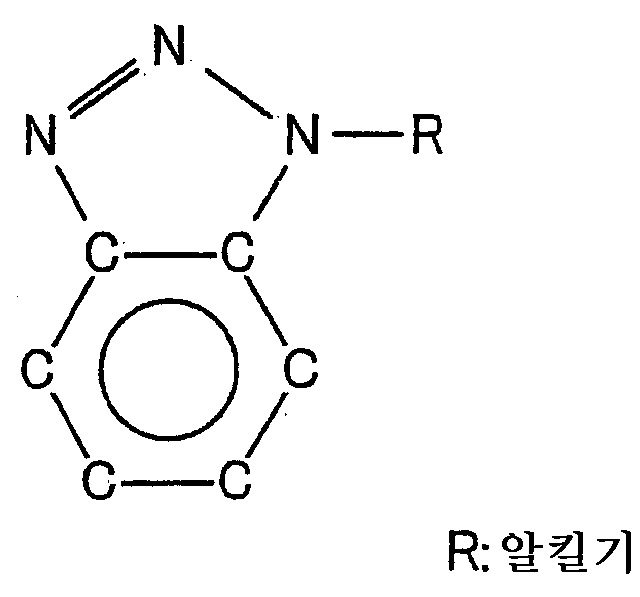
금속 이온 결합제로서는 벤조트리아졸계, 트리아진계 또는 이들의 이소시아누르 부가물류 등을 들 수 있다.Examples of the metal ion binders include benzotriazole-based, triazine-based or isocyanuric adducts thereof.
벤조트리아졸계는 하기 화학식 1로 표시되는 기본형의 벤조트리아졸을 시작으로, 메탄올의 부가물인 1H-벤조트리아졸-1-메탄올(화학식 2), 트리아졸 측에 알킬기를 부가한 것(화학식 3), 또는 벤젠 측에 알킬기를 부가한 것(화학식 4)을 들 수 있다.The benzotriazole type is obtained by adding an alkyl group to the triazole side, starting with benzotriazole of the basic type represented by the following general formula (1), which is an adduct of methanol, 1H-benzotriazole-1-methanol (Formula 2). Or an alkyl group added to the benzene side (Formula 4).
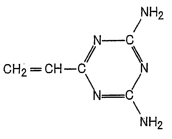
트리아진계는 화학식 5에 나타낸 것이며, 예를 들어 하기 화학식 6으로 표시되는 2,4-디아미노-6-비닐-S-트리아진, 하기 화학식 7로 표시되는 2,4-디아미노-6-[2'-에틸-4-메틸이미다졸-(1)]-에틸-S-트리아진, 또는 하기 화학식 8로 표시되는 2,4-디아미노-6-메타크릴로일옥시에틸-S-트리아진을 들 수 있다.The triazine is represented by the formula (5), for example, 2,4-diamino-6-vinyl-S-triazine represented by the following formula (6), 2,4-diamino-6- [represented by the formula (7) 2'-ethyl-4-methylimidazole- (1)]-ethyl-S-triazine or 2,4-diamino-6-methacryloyloxyethyl-S-tri represented by the following formula (8) Ajin can be mentioned.


이소시아누르산 부가물은 상기한 트리아진계 또는 벤조트리아졸계의 화합물에 화학식 9에 나타낸 이소시아누르산을 부가한 것이다. 트리아진계의 화합물의 이소시아누르산 부가물은 화학식 10으로 표시되며, 예를 들어 화학식 11로 표시되는 2,4-디아미노-6-비닐-S-트리아진·이소시아누르산 또는 화학식 12로 표시되는 2,4-디아미노-6-메타크릴로일옥시에틸-S-트리아진을 들 수 있다.The isocyanuric acid adduct is the addition of the isocyanuric acid represented by the formula (9) to the above-described triazine-based or benzotriazole-based compound. The isocyanuric acid adduct of the triazine-based compound is represented by the formula (10), for example, 2,4-diamino-6-vinyl-S-triazine-isocyanuric acid or the formula (12) 2,4-diamino-6-methacryloyloxyethyl-S-triazine which is represented is mentioned.
이하에 이러한 금속 이온 결합제의 마이그레이션 억제 효과를 조사한 실험에 대해 설명한다. 실험에는 도 5(a)에 나타낸 전기 절연성 측정용의 빗살 모양의 배선 패턴을 사용했다. 빗살 모양의 배선 패턴은 폴리이미드를 포함하는 기판(30)에, 음극에 접속시킨 빗살 모양의 전극(31a)과 양극에 접속시킨 빗살 모양의 전극(31b)을 서로의 간격(도 5(b)의 거리 C)이 30 ㎛가 되도록 형성시킨 것이다. 또한, 빗살 모양의 전극(31a, 31b)은 두께 8 ㎛의 구리 위에 주석 도금을 실시한 것이다.The experiment which investigated the migration suppression effect of such a metal ion binder is demonstrated below. In the experiment, a comb-tooth shaped wiring pattern for measuring electrical insulation shown in Fig. 5A was used. In the comb-tooth shaped wiring pattern, a gap between the comb-shaped
이러한 빗살 모양의 배선 패턴은 반도체 장치의 배선 패턴과 동등한 것이며, 반도체 장치에 있어서 배선의 마이그레이션이 쉽게 발생하는 정도를 모의적으로 관찰할 수 있어, 마이그레이션을 누설 전류로서 측정할 수 있다. 즉, 빗살 모양의 전극(31a, 31b)으로부터 유출된 금속 이온이 석출되어 마이그레이션을 일으키면, 도 6에 나타낸 바와 같이 빗살 모양의 전극(31a)과 (31b)와의 사이에 금속이 성장하여 최종적으로는 빗살 모양의 전극(31a)과 (31b)가 접속된다. 이 때에, 빗살 모양의 전극(31a 및 31b)에 전압을 인가하면, 누설 전류가 급증하는 것으로부터 누설 전류를 측정함으로써 빗살 모양의 전극(31a)과 (31b)와의 접속을 관측할 수 있다.Such a comb-tooth shaped wiring pattern is equivalent to the wiring pattern of a semiconductor device, and can simulate the extent to which wiring migration easily occurs in a semiconductor device, and can measure migration as a leakage current. That is, when metal ions flowing out from the comb-shaped
실험에서는, 표 1에 나타낸 금속 이온 결합제를 소정의 농도가 되도록 순수한 물에 분산시켜, 빗살 모양의 배선 패턴에 전면·균일하게 소정량을 적하하였다. 적하 후, 빗살 모양의 전극(31a, 31b)에 소정의 직류 전압을 인가하고, 그 후에 실내 환경에서 방치하여 소정 시간마다 누설 전류치의 변화를 측정했다. 결과를 하기 표 1에 나타내었다.In experiment, the metal ion binder shown in Table 1 was disperse | distributed to pure water so that it may become a predetermined | prescribed density | concentration, and predetermined amount was dripped all over and uniformly to the comb-tooth shaped wiring pattern. After dripping, the predetermined | prescribed DC voltage was applied to the comb-shaped
이에 따르면, 비교예의 순수한 물에서는 마이그레이션 억제 효과가 전혀 없고, 벤조트리아졸, 1H-벤조트리아졸-1-메탄올, 2,4-디아미노-6-비닐-S-트리아진·이소시아누르산에 대해서는 매우 양호한 마이그레이션 억제 효과가 있었다. 또한, 2,4-디아미노-6-메타크릴로일옥시에틸-S-트리아진·이소시아누르산, 2,4-디아미노-6-[2'-에틸-4-메틸이미다졸-(1)]-에틸-S-트리아진에 대해서도 마이그레이션 억제 효과가 있었다. 또한, 2-비닐-4,6디아미노-S-트리아진에도 약간의 마이그레이션 억제 효과가 확인되었다.According to this, there is no migration inhibitory effect in the pure water of a comparative example, and it has no effect on a benzotriazole, 1H- benzotriazole-1-methanol, 2, 4- diamino-6-vinyl-S-triazine- isocyanuric acid. It had a very good migration suppression effect. Furthermore, 2,4-diamino-6-methacryloyloxyethyl-S-triazine isocyanuric acid, 2,4-diamino-6- [2'-ethyl-4-methylimidazole- (1)]-ethyl-S-triazine also had a migration inhibitory effect. In addition, a slight migration inhibitory effect was also observed in 2-vinyl-4,6diamino-S-triazine.
다음에, 마이그레이션 억제 효과가 매우 우수한 금속 이온 결합제에 대해서 수지와의 용해(혼합에 의해 응집되지 않고 분산될 수 있는 성질)를 조사한 결과, 벤조트리아졸, 1H-벤조트리아졸-1-메탄올은 수지와의 상용성이 좋아 양호하게 수지 중에 분산되었다. 한편, 2,4-디아미노-6-메타크릴로일옥시에틸-S-트리아진·이소시아누르산은 수지와의 상용성이 불량하여 수지 중에 분산하기 어려웠다.Next, as a result of investigating the dissolution with the resin (the property that can be dispersed without being aggregated by mixing) with respect to the metal ion binder having a very excellent migration inhibitory effect, benzotriazole and 1H-benzotriazole-1-methanol are resins. The compatibility with was good, and it disperse | distributed favorably in resin. On the other hand, 2,4-diamino-6-methacryloyloxyethyl-S-triazine isocyanuric acid was poor in compatibility with resin, and was difficult to disperse in resin.
이러한 수지 성분과의 상용성이 불량한 금속 이온 결합제를 수지 성분에 혼합시키면, 봉지 수지 중에 분산되지 않고 응집하여, 금속 이온 결합제가 불균일하게 존재하는 상태가 된다. 특히, 2,4-디아미노-6-비닐-S-트리아진·이소시아누르산 부가물은 산 무수물 등의 수지 성분과 혼합되기 어렵고, 응집을 일으키기 쉽다. 따라서, 이러한 수지, 예를 들어 봉지 수지(6)로서 사용했을 경우에, 부분적으로 금속 이온의 포착이 일어나기 어려운 부분이 생긴다.When a metal ion binder having poor compatibility with such a resin component is mixed with the resin component, it is aggregated without being dispersed in the encapsulating resin, resulting in a state in which the metal ion binder is unevenly present. In particular, 2,4-diamino-6-vinyl-S-triazine isocyanuric acid adduct is hard to mix with resin components, such as an acid anhydride, and it is easy to produce aggregation. Therefore, when used as such resin, for example, the sealing
따라서, 금속 이온 결합제로서 2,4-디아미노-6-비닐-S-트리아진·이소시아누르산 부가물과 같이 수지 중에 분산되기 어려운 금속 이온 결합제를 사용하는 경우, 금속 이온 결합제의 미분쇄화 및 균일한 분산·혼합이 필요하다. 이 때, 금속 이온 결합제를 평균 직경이 0.5 ㎛ 이하가 될 때까지 미분쇄화하는 것이 바람직하며, 1 ㎛ 이하로 하는 것이 보다 바람직하다. 또한, 금속 이온 결합제의 응집을 방지하기 위해서, 1 ㎛ 메쉬의 미세 컷 필터에 의한 여과 처리를 실시하는 것도 유효하다. 또한, 금속 이온 결합제의 미분쇄 및 균일한 분산을 위한 혼합 방법으로서는, 봉지 수지의 혼련을 롤 밀 장치 또는 비드 밀 장치를 사용하여 분쇄, 혼합 처리를 실시하는 것이 바람직하다.Therefore, in the case of using a metal ion binder which is hard to be dispersed in a resin such as 2,4-diamino-6-vinyl-S-triazine-isocyanuric acid adduct as the metal ion binder, finely pulverizing the metal ion binder And uniform dispersion and mixing are necessary. At this time, it is preferable to grind | pulverize a metal ion binder until it becomes 0.5 micrometer or less in average diameter, and it is more preferable to set it as 1 micrometer or less. Moreover, in order to prevent aggregation of a metal ion binder, it is also effective to perform the filtration process by the fine cut filter of a 1 micrometer mesh. Moreover, as a mixing method for the fine grinding and uniform dispersion of a metal ion binder, it is preferable to grind and mix processing of sealing resin using a roll mill apparatus or a bead mill apparatus.
다음에, 금속 이온 결합제를 봉지 수지(6)에 혼합시키는 경우를 예로 들어 금속 이온 결합제를 혼합한 봉지 수지 재료의 제조에 대해 설명한다.Next, the manufacture of the sealing resin material which mixed the metal ion binder is demonstrated, taking the case where the metal ion binder is mixed in the sealing
봉지 수지(6)의 수지 성분으로서는, 에폭시 수지 또는 산 무수물 등이 사용된다. 이것에 미세 분체상의 상기한 금속 이온 결합제, 염료, 경화 촉진제를 첨가하여 혼련한다. 배합비로서는, 예를 들어 에폭시 수지 및 경화제를 99.6 중량%, 금속 이온 결합제를 2.5 중량%, 염료 및 경화 촉진제를 0.9 중량%로 하는 것이 바람직하다.As the resin component of the sealing
여기서, 봉지 수지(6)에 있어서, 양호하게 마이그레이션을 억제할 수 있음과 동시에 양호한 유동성을 얻을 수 있는 금속 이온 결합제의 함유량을 조사했다.Here, in the sealing
먼저, 마이그레이션 억제 기능을 발휘하기 위해 필요한 금속 이온 결합제의 함유량을 조사했다. 실험 방법으로서는, 에폭시 수지에 금속 이온 결합제로서 2,4-디아미노-6-비닐-S-트리아진·이소시아누르산 부가물이 0, 0.5, 1.5, 2.5, 5.0, 10.0, 15.0 중량%가 되도록 첨가한 수지를 준비하여, 도 5(a) 및 도 5(b)의 빗살 모양의 배선 패턴 전면에 균일하게 피복하고, 직류 전압 40 V를 인가하면서 85 ℃ 분위기 하, 85% RH의 환경 하에 방치하여 누설 전류를 조사했다. 여기서, 금속 이온 결합제와 수지와의 혼합에는, 롤 밀 또는 비드 밀 장치를 사용했다. 또한, 이러한 수지는 주요 구성으로서 에폭시 수지 및 금속 이온 결합제로 구성되어 있고, 금속 이온 결합제 0 중량%인 경우는 에폭시 수지 및 경화제가 99.3 중량%, 염료 및 경화 촉진제가 0.7 중량% 포함되어 있는 것을 사용했다.First, the content of the metal ion binder required to exhibit the migration suppression function was investigated. As an experimental method, 0, 0.5, 1.5, 2.5, 5.0, 10.0, and 15.0 weight% of 2,4-diamino-6-vinyl-S-triazine isocyanuric acid addition product were added to the epoxy resin as a metal ion binder. Resin added as necessary, was uniformly coated on the entire surface of the comb-toothed wiring pattern of FIGS. 5 (a) and 5 (b), and applied under a DC voltage of 40 V under 85 ° C. atmosphere under 85% RH. It was left to stand and the leakage current was examined. Here, the roll mill or the bead mill apparatus was used for mixing a metal ion binder and resin. In addition, such a resin is composed of an epoxy resin and a metal ion binder as main components, and in the case of 0 wt% of a metal ion binder, a 99.3 wt% epoxy resin and a curing agent and 0.7 wt% of a dye and a curing accelerator are used. did.
결과를 도 7에 나타내었다. 도 7의 횡축은 방치 시간이며, 종축은 누설 전류로부터 계산되는 빗살 모양의 전극(31a, 31b) 사이의 절연 저항값의 변화를 측정한 결과이다. 이에 따르면, 금속 이온 결합제 무첨가의 수지에서는, 500시간 후에 배선으로부터 발생한 구리의 석출에 기인하는 마이그레이션에 의해, 절연 파괴가 발생하였다. 한편, 금속 이온 결합제를 0.5% 첨가한 수지에서는 700시간 후까지 절연 파괴가 일어나지 않아, 배선(9)의 마이그레이션이 늦추어진 것을 알 수 있었다. 그리고, 금속 이온 결합제를 1.5% 포함하는 수지에서는 900시간 후까지 양호한 절연성이 유지된 후에, 절연성이 저하하였다. 따라서, 절연성의 저하가 더욱 지연되고, 또한 관측한 1000시간까지 절연성이 완전하게 파괴되는 일이 없었다. 그 밖의 금속 이온 결합제의 첨가량이 2.5 중량% 이상인 수지에서는 관측한 1000시간 후에도 전기 절연성이 안정되어 있었다. 즉, 금속 이온 결합제의 첨가량이 많아질수록, 고온 고습도 환경 하에서도 전기 절연성이 양호하다는 것을 알 수 있었다. 따라서, 금속 이온 결합제를 포함하는 수지를 도포하여 양호한 마이그레이션 억제 효과를 얻기 위해서는, 수지가 금속 이온 결합제를 0.5 중량% 이상 포함하는 것이 바람직하고, 특히 2.5 중량% 이상 포함하는 것이 바람직하다고 할 수 있다.The results are shown in FIG. 7 represents the leaving time, and the vertical axis represents the result of measuring the change in the insulation resistance value between the comb-shaped
다음에, 봉지 수지에 필요한 유동성을 유지할 수 있는 금속 이온 결합제에의 함유량을 조사했다. 즉, 상기한 금속 이온 결합제는 금속 이온과 착체를 형성하는 기능을 갖는 한편, 수지와 혼합했을 경우에, 그 분자 구조로 인해 수지의 경화를 촉진시킨다. 따라서, 금속 이온 결합제를 봉지 수지(6)에 너무 많이 혼합하면, 봉지 수지(6)의 점도가 과도하게 상승하여 봉지 수지(6)의 충전이 어려워진다. 즉, 봉지 수지(6)는 분배기에 의해 반도체 칩(5)과 가요성 배선 기판(10)과의 사이에 충전되지만, 봉지 수지(6)의 점도가 높으면 분배기로부터의 안정 토출이 이루어질 수 없게 된다. 또한, 봉지 수지는 그의 유동성에 의해 반도체 칩(5)과 가요성 배선 기판(10)과의 사이를 빈틈없이 충전하는 것인데, 봉지 수지(6)의 점도가 높으면 유동성이 낮아져 반도체 칩(5)과 가요성 배선 기판(10)과의 사이에 봉지 수지를 빈틈없이 충전할 수 없게 된다. 따라서, 봉지 수지(6)에 금속 이온 결합제를 혼합하는 경우, 점도의 상승을 고려하여 유동성이 손상되지 않도록 할 필요가 있다. 또한, 중점적으로 적절한 봉지 수지(6)의 점도로서는 50 mPa·s 이상 1250 mPa·s 이하이며, 보다 바람직하게는 200 mPa·s 이상 1000 mPa·s 이하이다.Next, the content to the metal ion binder which can maintain the fluidity required for sealing resin was investigated. That is, the above metal ion binder has a function of forming a complex with metal ions, and when mixed with the resin, the molecular structure promotes curing of the resin. Therefore, when too much metal ion binder is mixed with the sealing
이를 위해서는, 봉지 수지(6)에 대해 10 중량% 이하가 되도록 혼합하는 것이 바람직하며, 5 중량% 이하가 되도록 혼합하는 것이 보다 바람직하다.For this purpose, it is preferable to mix so that it may become 10 weight% or less with respect to the sealing
여기서, 에폭시 수지에 금속 이온 결합제로서 2,4-디아미노-6-비닐-S-트리아진·이소시아누르산 부가물을 0 중량% 내지 15 중량% 첨가한 봉지 수지의 점도를 측정한 결과를 하기 표 2에 나타낸다. 단, 여기서 사용하는 봉지 수지는 주요 구성으로서 에폭시 수지 및 금속 이온 결합제로 구성되어 있다.Here, the result of having measured the viscosity of the sealing resin which added 0 weight%-15 weight% of 2, 4- diamino-6-vinyl-S-triazine- isocyanuric acid adduct to a epoxy ion as a metal ion binder. It is shown in Table 2 below. However, the sealing resin used here consists of an epoxy resin and a metal ion binder as a main structure.
이에 따르면, 금속 이온 결합제를 포함하지 않는 봉지 수지(0 중량%)가 점도 850 mPa·s인 것에 비해, 금속 이온 결합제의 첨가량에 따라 봉지 수지의 점도가 증대되고 있다. 금속 이온 결합제가 5 중량% 이하일 때는, 점도가 1000 mPa·s보다 낮고, 수지 토출성(분배기로부터 수지가 양호하게 흘러나오는 성질) 및 충전성(반도체 칩(5)과 가요성 배선 기판(10)과의 사이를 빈틈없이 충전할 수 있는 성질)이 양호하다. 그러나, 금속 이온 결합제가 10 중량%일 때는, 점도가 1250 mPa·s가 되어 수지 토출 안정성, 충전성이 약간 손상된다. 그리고, 금속 이온 결합제가 15 중량%가 되면, 점도가 1500 mPa·s가 되어 분배기로부터의 수지 토출이 순조롭게 못하게 된다. 또한, 반도체 칩(5)과 가요성 배선 기판(10)의 사이에 충전하면, 도 8에 나타낸 바와 같이 부분적으로 충전할 수 없는 부분이 발생하여 이 부분에 기포(21)가 생성되어 버린다. 이와 같이, 반도체 칩(5)과 가요성 배선 기판(10)과의 사이에 기포(21)가 생성되면, 반도체 칩(5)이 확실하게 가요성 배선 기판(10)에 고정되지 않아 접속 불량을 일으킬 가능성이 있다. 또한, 기포에 수분이 모여 반도체 칩 보호의 신뢰성 저하를 초래할 가능성이 있다.According to this, while the sealing resin (0 weight%) which does not contain a metal ion binder is 850 mPa * s, the viscosity of sealing resin increases with the addition amount of a metal ion binder. When the metal ion binder is 5% by weight or less, the viscosity is lower than 1000 mPa · s, and the resin discharging property (the property that the resin flows well from the distributor) and the filling property (
또한, 봉지 수지의 점도 증가의 억제를 위해서는, 봉지 수지에 사용하는 경화 촉진제의 작용을 조정하는 방법도 있다. 예를 들어 경화 촉진제의 성분을 캡슐에 스며들게 함으로써 저온 시에 경화 반응을 억제하거나, 경화 촉진제의 분자 구조의 조정에 의해 저온 시에 있어서의 경화 반응을 억제하는 것을 생각할 수 있다.Moreover, in order to suppress the increase of the viscosity of sealing resin, there also exists a method of adjusting the action | action of the hardening accelerator used for sealing resin. For example, it is conceivable to suppress the curing reaction at low temperature by infiltrating a component of the curing accelerator into the capsule or to suppress the curing reaction at low temperature by adjusting the molecular structure of the curing accelerator.
또한, 봉지 수지의 점도 또는 첨가하는 효과 촉진제를 조정함으로써 수지 수명의 단축, 불순물 이온 농도의 증가를 방지하여도 된다.In addition, by adjusting the viscosity of the sealing resin or the effect promoter to be added, the shortening of the resin life and the increase of the impurity ion concentration may be prevented.
또한, 금속 이온 결합제를 솔더 레지스트(7)에 혼합하는 경우, 솔더 레지스트(7)의 재료가 경화되기 전 상태에서, 0.5 중량% 이상의 금속 이온 결합제를 혼합하고, 그 이후에 경화시킴으로써 배선(9)의 마이그레이션을 억제할 수 있는 솔더 레지스트가 된다. 또한, 솔더 레지스트(7)는 인쇄되어 형성되는 경우, 인쇄에 적절한 특성이 되도록 금속 이온 결합제의 혼합을 10.0 중량% 이하로 하는 것이 바람직하다.In addition, when mixing a metal ion binder with the soldering resist 7, in the state before the material of the soldering resist 7 hardens, 0.5 weight% or more of a metal ion binder is mixed, and it hardens after that
또한, 금속 이온 결합제를 베이스 필름(1)에 혼합하는 경우, 베이스 필름(1)의 재료가 경화되기 전에, 0.5 중량% 이상의 금속 이온 결합제를 혼합하고, 그 이후에 경화시킴으로써 배선(9)의 마이그레이션을 억제할 수 있다. 또한, 이 경우에는, 재료 특성을 확보하기 위해서 금속 이온 결합제의 혼합을 10.0 중량% 이하로 하는 것이 바람직하다.In addition, when mixing a metal ion binder with the
또한, 금속 이온 결합제를 배선(9)에 도포하는 경우, 용제로서 예를 들어 순수한 물을 사용하여 0.5 중량% 이상의 금속 이온 결합제를 혼합하는 것이 바람직하다. 이것에 의해 배선(9)의 마이그레이션을 억제할 수 있다.In addition, when apply | coating a metal ion binder to
본 발명은 이상과 같이 미세 피치화된 배선에 있어서도, 인접하는 배선과의 절연 파괴를 억제할 수 있다. 따라서, 배선의 미세 피치화 및 고전압화가 요구되고 있는, 기재가 가요성 기판인 반도체 장치, 테이프 캐리어 방식의 반도체 장치, 액정 표시 장치를 탑재한 반도체 장치에 특히 바람직하게 적용될 수 있다.In the present invention, even in the fine pitched wiring, insulation breakdown with adjacent wirings can be suppressed. Therefore, the substrate can be particularly preferably applied to a semiconductor device in which a substrate is a flexible substrate, a tape carrier type semiconductor device, and a liquid crystal display device, in which fine pitch and high voltage of wiring are required.
또한, 본 발명은 상술한 각각의 실시 형태로 한정되는 것이 아니고, 청구항에 나타낸 범위에서 다양한 변경이 가능하며, 상이한 실시 형태에 각각 개시된 기술적 수단을 적당히 조합하여 얻을 수 있는 실시 형태도 본 발명의 기술적 범위에 포함된다.In addition, this invention is not limited to each above-mentioned embodiment, Various changes are possible in the range shown to the claim, The embodiment which can be obtained by combining suitably the technical means disclosed respectively in the different embodiment is also technical of this invention. It is included in a range.
또한, 본 발명은 이하의 구성으로 할 수도 있다.In addition, this invention can also be set as the following structures.
배선 패턴이 형성된 필름상의 가요성 기판에 반도체 소자가 탑재된 반도체 장치에 있어서, 배선 패턴 간의 전기 절연 특성을 향상시키기 위해 반도체 칩 보호용의 봉지 수지 내, 또는 솔더 레지스트 내, 또는 베이스 기재 내에 마이그레이션 억제제(금속 이온 결합제)를 첨가·혼합 또는 배선 패턴 표면에 도포한 것을 특징으로 하는 제1의 반도체 장치.In a semiconductor device in which a semiconductor element is mounted on a film-like flexible substrate on which a wiring pattern is formed, a migration inhibitor in a sealing resin for protecting a semiconductor chip, a solder resist, or a base substrate in order to improve electrical insulation between wiring patterns. 1st semiconductor device characterized by adding and mixing a metal ion binder), or apply | coating to the wiring pattern surface.
상기 제1의 반도체 장치에 있어서, 사용하는 마이그레이션 억제제가 벤조트리아졸류, 트리아진류, 이소시아누르산류, 트리아진류 및 이소시아누르산 부가물의 조성을 갖는 물질을 봉지 수지 또는 솔더 레지스트 또는 베이스 기재 내에 첨가·혼합 또는 배선 패턴 표면에 도포한 것을 특징으로 하는 제2의 반도체 장치.In the first semiconductor device, a migration inhibitor to be used is added to an encapsulating resin, solder resist, or base substrate with a substance having a composition of benzotriazoles, triazines, isocyanuric acids, triazines and isocyanuric acid adducts. The second semiconductor device is coated on the mixed or wiring pattern surface.
상기 제1 또는 제2의 반도체 장치에 있어서, 사용하는 마이그레이션 억제제를 첨가할 때에 발생하는 수지의 고점도화 및 마이그레이션 억제제의 응집을 억제하기 위해, 봉지 수지 또는 솔더 레지스트 또는 베이스 기재 내에 상기 마이그레이션 억제제를 0.5 내지 10.0 중량% 첨가·혼합한 재료를 사용하는 것을 특징으로 하는 제3의 반도체 장치.In the first or second semiconductor device, in order to suppress the high viscosity of the resin and the aggregation of the migration inhibitor occurring when the migration inhibitor is used, 0.5 or less of the migration inhibitor is contained in the encapsulating resin or the solder resist or the base substrate. To 10.0 wt% added and mixed with a material, the third semiconductor device characterized by the above-mentioned.
상기 제1의 반도체 장치에 있어서, 보호용의 봉지 수지로서 사용하는 마이그레이션 억제제에 대해 수지 내에 첨가할 때에 발생하는 고점도화를 억제하기 위해, 증점도 억제 효과를 갖는 경화 촉진제를 사용하고, 점도 조정을 실시한 점도 50 내지 1250 mPa·s의 봉지 수지로 보호되고 있는 것을 특징으로 하는 제4의 반도체 장치.In the said 1st semiconductor device, in order to suppress the high viscosity which arises when it adds in resin with respect to the migration inhibitor used as sealing resin for protection, the viscosity adjustment was performed using the hardening accelerator which has a thickening inhibitory effect. The fourth semiconductor device is protected by a sealing resin having a viscosity of 50 to 1250 mPa · s.
배선 패턴이 형성된 필름상의 가요성 기판에 반도체 소자가 탑재된 반도체 장치에 있어서, 배선 패턴 간의 전기 절연 특성을 향상시키기 위해, 가요성 기판 상의 배선 패턴 표면에 마이그레이션 억제제를 사용하여 표면 처리(마이그레이션 억제제를 함침 또는 분무)하고, 배선 패턴 표면에 마이그레이션 억제제를 도포한 가요성 기판을 사용하는 것을 특징으로 하는 제5의 반도체 장치.In a semiconductor device in which a semiconductor element is mounted on a film-like flexible substrate on which a wiring pattern is formed, in order to improve electrical insulation between the wiring patterns, a surface inhibitor (migration inhibitor) is used on the surface of the wiring pattern on the flexible substrate using a migration inhibitor. Impregnated or sprayed), and a flexible substrate having a migration inhibitor applied to the wiring pattern surface is used.
상기 제1 내지 5의 반도체 장치에 있어서, 필름상의 가요성 기판이 길이가 긴 테이프상이며, 반도체 소자가 연속적으로 가요성 기판에 탑재된 테이프 캐리어형의 반도체 장치인 것을 특징으로 하는 제6의 반도체 장치.In the first to fifth semiconductor devices, the film-like flexible substrate is a long tape, and the semiconductor element is a tape carrier-type semiconductor device in which the semiconductor element is continuously mounted on the flexible substrate. Device.
상기 제1 내지 5의 반도체 장치에 있어서, 액정 표시 소자 또는 주변 부품이 탑재된 액정 모듈의 반도체 장치인 것을 특징으로 하는 제7의 반도체 장치.The seventh semiconductor device according to the first to fifth semiconductor devices, wherein the liquid crystal display device or the peripheral component is a semiconductor device of a liquid crystal module.
본 발명의 반도체 장치는 배선으로부터의 금속의 석출을 방지하고, 배선 간의 절연 파괴를 방지할 수 있으므로, 특히 배선 피치가 좁은 반도체 장치에 매우 적합하며, 예를 들어 기재가 가요성 기판인 반도체 장치, 테이프 캐리어 방식의 반도체 장치, 액정 표시 장치를 탑재한 반도체 장치에 적용할 수 있다.Since the semiconductor device of the present invention can prevent the deposition of metal from the wiring and prevent breakdown between the wirings, the semiconductor device is particularly suitable for a semiconductor device having a narrow wiring pitch, for example, a semiconductor device whose substrate is a flexible substrate, It can be applied to a semiconductor device having a tape carrier system semiconductor device and a liquid crystal display device.
본 발명의 반도체 장치는 이상과 같이 기재에 복수의 배선이 배치된 배선 기판, 및 상기 배선 기판에 탑재된 반도체 소자를 포함하는 반도체 장치에 있어서, 금속 이온 결합제가 상기 배선과 접하는 부재의 재료에 혼합되어 있거나, 또는 상기 배선 표면에 첨가되어 있다.The semiconductor device of the present invention comprises a wiring board having a plurality of wirings arranged on a substrate as described above, and a semiconductor device mounted on the wiring board, wherein the metal ion binder is mixed with the material of the member in contact with the wiring. Or is added to the wiring surface.
이에 따라, 배선으로부터 방출된 재료의 금속 이온이 배선과 접하는 부재에 포함되거나, 또는 배선 표면에 첨가되는 금속 이온 결합제와 접촉하여 금속 이온을 포착함으로써 금속 이온이 석출되는 것을 방지할 수 있다. 따라서, 배선으로부터의 금속의 성장도 방지되므로, 반도체 장치의 동작 불량을 방지할 수 있다.As a result, the metal ions of the material released from the wiring can be contained in the member in contact with the wiring, or the metal ions can be prevented from being deposited by contacting the metal ion binder added to the wiring surface to trap the metal ions. Therefore, the growth of the metal from the wiring is also prevented, so that a malfunction of the semiconductor device can be prevented.
또한, 발명의 상세한 설명의 항에서 실시한 구체적인 실시 형태, 또는 실시예는 어디까지나 본 발명의 기술적 내용을 분명히 하기 위한 것이며, 이러한 구체예에만 한정되는 좁은 뜻으로 해석되어야 할 것이 아니라, 본 발명의 정신과 이어서 기재할 특허 청구항의 범위 내에서 다양하게 변경하여 실시할 수 있는 것이다.In addition, the specific embodiment implemented in the term of the detailed description of the invention, or the Example is for the clarity of the technical content of this invention to the last, and is not to be interpreted by the narrow meaning limited only to this specific example, Subsequently, various changes can be made within the scope of the patent claims to be described.
본 발명에 의하면, 종래의 반도체 장치에 있어서 봉지 수지에 금속 이온 결합제를 첨가하는 것만으로 배선으로부터의 금속 이온의 석출을 방지할 수 있다. 그 결과, 배선으로부터의 금속의 성장이 방지되어 반도체 장치의 동작 불량이 방지된다. 또한, 본 발명에 의하면 부가적으로 배선 표면에 솔더 레지스트가 형성되어 있는 반도체 장치에서 제조 공정 또는 부재의 수를 증가시키는 일 없이, 솔더 레지스트의 재료에 금속 이온 결합제를 첨가하는 것만으로 배선으로부터의 금속의 성장도 방지되고 반도체 장치의 동작 불량이 방지된다.According to the present invention, in the conventional semiconductor device, it is possible to prevent the precipitation of metal ions from the wiring simply by adding the metal ion binder to the sealing resin. As a result, growth of metal from the wiring is prevented, and a malfunction of the semiconductor device is prevented. In addition, according to the present invention, in a semiconductor device in which a solder resist is formed on the wiring surface, the metal from the wiring can be added simply by adding a metal ion binder to the material of the solder resist without increasing the number of manufacturing processes or members. Growth of the semiconductor device is prevented and poor operation of the semiconductor device is prevented.
Claims (11)
Applications Claiming Priority (2)
| Application Number | Priority Date | Filing Date | Title |
|---|---|---|---|
| JPJP-P-2004-00152372 | 2004-05-21 | ||
| JP2004152372A JP4451214B2 (en) | 2004-05-21 | 2004-05-21 | Semiconductor device |
Publications (2)
| Publication Number | Publication Date |
|---|---|
| KR20060048036A KR20060048036A (en) | 2006-05-18 |
| KR100728852B1 true KR100728852B1 (en) | 2007-06-15 |
Family
ID=35424288
Family Applications (1)
| Application Number | Title | Priority Date | Filing Date |
|---|---|---|---|
| KR1020050042307A Expired - Lifetime KR100728852B1 (en) | 2004-05-21 | 2005-05-20 | Semiconductor device |
Country Status (5)
| Country | Link |
|---|---|
| US (1) | US7474008B2 (en) |
| JP (1) | JP4451214B2 (en) |
| KR (1) | KR100728852B1 (en) |
| CN (1) | CN100397625C (en) |
| TW (1) | TWI267534B (en) |
Families Citing this family (27)
| Publication number | Priority date | Publication date | Assignee | Title |
|---|---|---|---|---|
| US11842972B2 (en) | 2004-09-28 | 2023-12-12 | Rohm Co., Ltd. | Semiconductor device with a semiconductor chip connected in a flip chip manner |
| JP2006100385A (en) * | 2004-09-28 | 2006-04-13 | Rohm Co Ltd | Semiconductor device |
| KR101144557B1 (en) * | 2006-03-27 | 2012-05-11 | 엘지이노텍 주식회사 | Lighting Device with Light Emitting Diodes and manufacture method thereof |
| JP4219953B2 (en) * | 2006-12-11 | 2009-02-04 | シャープ株式会社 | IC chip mounting package and manufacturing method thereof |
| JP2008289510A (en) * | 2007-05-22 | 2008-12-04 | Daito Giken:Kk | Game table |
| KR20080108767A (en) * | 2007-06-11 | 2008-12-16 | 삼성에스디아이 주식회사 | Electrode terminal coating material and plasma display panel |
| JP4518128B2 (en) * | 2007-10-01 | 2010-08-04 | 株式会社デンソー | Electronic circuit device manufacturing method and electronic circuit device |
| WO2009149249A1 (en) * | 2008-06-06 | 2009-12-10 | Cima Nanotech Israel Ltd. | Processes for making transparent conductive coatings |
| US7898074B2 (en) | 2008-12-12 | 2011-03-01 | Helmut Eckhardt | Electronic devices including flexible electrical circuits and related methods |
| JP2010239022A (en) * | 2009-03-31 | 2010-10-21 | Mitsui Mining & Smelting Co Ltd | Flexible printed wiring board and semiconductor device using the same |
| JP5647769B2 (en) * | 2009-05-13 | 2015-01-07 | ナミックス株式会社 | COF sealing resin composition |
| JP2011178986A (en) * | 2010-02-02 | 2011-09-15 | Nitto Denko Corp | Adhesive composition for production of semiconductor device and adhesive sheet for production of semiconductor device |
| TWI399818B (en) * | 2010-04-14 | 2013-06-21 | 力成科技股份有限公司 | Semiconductor package structure for blocking metal ions from being emitted to a wafer |
| US8552333B2 (en) | 2010-12-30 | 2013-10-08 | General Electric Company | Systems, methods, and apparatus for preventing electromigration between plasma gun electrodes |
| US20120267779A1 (en) | 2011-04-25 | 2012-10-25 | Mediatek Inc. | Semiconductor package |
| JP2012231033A (en) * | 2011-04-26 | 2012-11-22 | Fujifilm Corp | Printed wiring board with surface coated wiring and manufacturing method thereof |
| WO2013035204A1 (en) | 2011-09-09 | 2013-03-14 | ヘンケル・アクチェンゲゼルシャフト・ウント・コムパニー・コマンディットゲゼルシャフト・アウフ・アクチェン | Composition for electronic device |
| WO2013035205A1 (en) | 2011-09-09 | 2013-03-14 | ヘンケル・アクチェンゲゼルシャフト・ウント・コムパニー・コマンディットゲゼルシャフト・アウフ・アクチェン | Underfill composition |
| JP2013118276A (en) * | 2011-12-02 | 2013-06-13 | Namics Corp | Semiconductor device |
| CN103378044A (en) * | 2012-04-25 | 2013-10-30 | 鸿富锦精密工业(深圳)有限公司 | Chip assembly structure and chip assembly method |
| US20130292819A1 (en) * | 2012-05-07 | 2013-11-07 | Novatek Microelectronics Corp. | Chip-on-film device |
| TWI509750B (en) * | 2013-09-30 | 2015-11-21 | Chipmos Technologies Inc | Multi-chip tape package structure |
| JP6242679B2 (en) | 2013-12-25 | 2017-12-06 | 日東電工株式会社 | Resin film for semiconductor device and method for manufacturing semiconductor device |
| JP2015126019A (en) | 2013-12-25 | 2015-07-06 | 日東電工株式会社 | Resin film for semiconductor device and method for manufacturing semiconductor device |
| WO2018159023A1 (en) * | 2017-03-01 | 2018-09-07 | 住友電気工業株式会社 | Flexible printed wiring board, method for manufacturing connector, and connector |
| CN108983477B (en) * | 2018-09-27 | 2021-04-02 | 武汉华星光电半导体显示技术有限公司 | Display module, manufacturing method thereof, and electronic device |
| CN110515273B (en) * | 2019-08-26 | 2023-07-14 | 江苏上达半导体有限公司 | Production and conveying method of COF tape |
Citations (3)
| Publication number | Priority date | Publication date | Assignee | Title |
|---|---|---|---|---|
| JPS62207320A (en) * | 1986-03-07 | 1987-09-11 | Hitachi Ltd | Theromosetting resin composition and semiconductor device coated or sealed therewith |
| JPH01294765A (en) * | 1988-05-20 | 1989-11-28 | Nippon Retsuku Kk | Epoxy resin composition |
| JP2003092379A (en) * | 2001-09-18 | 2003-03-28 | Hitachi Ltd | Semiconductor device |
Family Cites Families (17)
| Publication number | Priority date | Publication date | Assignee | Title |
|---|---|---|---|---|
| US1489577A (en) * | 1921-04-19 | 1924-04-08 | Bengt M W Hanson | Gauge |
| JPS53116391A (en) | 1977-03-18 | 1978-10-11 | Shikoku Kasei Kougiyou Kk | Novel imidazoleisocyanuric adduct synthesizing method thereof polyepoxy hardening method containing same as main component polyepoxy hardening method using same as hardening improver and method of pur |
| US4205156A (en) | 1977-03-18 | 1980-05-27 | Shikoku Chemicals Corporation | Novel imidazole-isocyanuric acid adducts and utilization thereof |
| JPS6112772A (en) | 1984-06-27 | 1986-01-21 | Shikoku Chem Corp | Epoxy resin ink composition |
| JPH06228308A (en) * | 1992-12-29 | 1994-08-16 | Internatl Business Mach Corp <Ibm> | Triazine polymer and its use |
| JP3065509B2 (en) * | 1995-06-02 | 2000-07-17 | スタンレー電気株式会社 | Surface mount type light emitting diode |
| JP3624512B2 (en) | 1996-01-12 | 2005-03-02 | イビデン株式会社 | Manufacturing method of electronic component mounting board |
| US6205657B1 (en) | 1996-11-08 | 2001-03-27 | Matsushita Electric Industrial Co., Ltd. | Printed circuit board and method for producing the same |
| JP3449889B2 (en) * | 1997-08-08 | 2003-09-22 | 住友ベークライト株式会社 | Anisotropic conductive adhesive |
| JPH1192740A (en) | 1997-09-24 | 1999-04-06 | Hitachi Chem Co Ltd | Resin paste composition and semiconductor device |
| JPH11144527A (en) | 1997-11-06 | 1999-05-28 | Matsushita Electric Ind Co Ltd | Conductive paste for bonding electronic components |
| JP2000103838A (en) | 1998-09-25 | 2000-04-11 | Nagase Chiba Kk | Epoxy resin composition for semiconductor sealing |
| JP2001316566A (en) | 2000-05-10 | 2001-11-16 | Nagase Chemtex Corp | One pack epoxy resin composition and epoxy resin composition for semiconductor sealing use using the same |
| JP3858705B2 (en) | 2001-01-29 | 2006-12-20 | 宇部興産株式会社 | Underfill material for COF mounting and electronic components |
| JP2002222897A (en) | 2001-01-29 | 2002-08-09 | Hitachi Metals Ltd | Semiconductor package |
| JP2002256443A (en) * | 2001-02-27 | 2002-09-11 | Japan Science & Technology Corp | Plating method |
| JP3847693B2 (en) * | 2002-09-30 | 2006-11-22 | シャープ株式会社 | Manufacturing method of semiconductor device |
-
2004
- 2004-05-21 JP JP2004152372A patent/JP4451214B2/en not_active Expired - Lifetime
-
2005
- 2005-05-20 KR KR1020050042307A patent/KR100728852B1/en not_active Expired - Lifetime
- 2005-05-20 TW TW094116520A patent/TWI267534B/en not_active IP Right Cessation
- 2005-05-20 US US11/133,379 patent/US7474008B2/en not_active Expired - Lifetime
- 2005-05-23 CN CNB2005100739141A patent/CN100397625C/en not_active Expired - Lifetime
Patent Citations (3)
| Publication number | Priority date | Publication date | Assignee | Title |
|---|---|---|---|---|
| JPS62207320A (en) * | 1986-03-07 | 1987-09-11 | Hitachi Ltd | Theromosetting resin composition and semiconductor device coated or sealed therewith |
| JPH01294765A (en) * | 1988-05-20 | 1989-11-28 | Nippon Retsuku Kk | Epoxy resin composition |
| JP2003092379A (en) * | 2001-09-18 | 2003-03-28 | Hitachi Ltd | Semiconductor device |
Also Published As
| Publication number | Publication date |
|---|---|
| TW200613431A (en) | 2006-05-01 |
| CN100397625C (en) | 2008-06-25 |
| TWI267534B (en) | 2006-12-01 |
| JP4451214B2 (en) | 2010-04-14 |
| US20050263909A1 (en) | 2005-12-01 |
| KR20060048036A (en) | 2006-05-18 |
| US7474008B2 (en) | 2009-01-06 |
| CN1707779A (en) | 2005-12-14 |
| JP2005333085A (en) | 2005-12-02 |
Similar Documents
| Publication | Publication Date | Title |
|---|---|---|
| KR100728852B1 (en) | Semiconductor device | |
| US6689639B2 (en) | Method of making semiconductor device | |
| CN112201435B (en) | Coil assembly and method of manufacturing the same | |
| US7189927B2 (en) | Electronic component with bump electrodes, and manufacturing method thereof | |
| US9345148B2 (en) | Semiconductor device and method of forming flipchip interconnection structure with bump on partial pad | |
| CN106914710B (en) | Resin flux paste and mounting structure | |
| US8039307B2 (en) | Mounted body and method for manufacturing the same | |
| US20040169288A1 (en) | Padless high density circuit board and manufacturing method thereof | |
| US20110074026A1 (en) | Semiconductor Device and Method of Forming Insulating Layer on Conductive Traces for Electrical Isolation in Fine Pitch Bonding | |
| KR20120061713A (en) | Semiconductor device and method of forming bump-on-lead interconnection | |
| JP5296116B2 (en) | Semiconductor device | |
| JP5014945B2 (en) | Semiconductor device | |
| US6800944B2 (en) | Power/ground ring substrate for integrated circuits | |
| KR20030024616A (en) | Semiconductor device | |
| TW201227901A (en) | Semiconductor device and method of self-confinement of conductive bump material during reflow without solder mask | |
| US7473476B2 (en) | Soldering method, component to be joined by the soldering method, and joining structure | |
| US7575994B2 (en) | Semiconductor device and manufacturing method of the same | |
| US20060289991A1 (en) | Semiconductor device and manufacturing method of the same | |
| KR100374075B1 (en) | Film carrier tape for mounting electronic parts and method for manufacturing the same | |
| US11616007B2 (en) | Electronic package | |
| JP4644963B2 (en) | Curing flux and solder joint | |
| Phosri et al. | Galvanic corrosion behavior of Ag-filled electrically conductive adhesive on Sn-plated of surface mount chip resistor | |
| Li et al. | Recent advances of conductive adhesives: A lead-free alternative in electronic packaging | |
| KR20120062599A (en) | Semiconductor device and method of forming narrow interconnect sites on substrate with elongated mask openings | |
| US20130029458A1 (en) | Substrate for semiconductor package having coating film and method for manufacturing the same |
Legal Events
| Date | Code | Title | Description |
|---|---|---|---|
| A201 | Request for examination | ||
| PA0109 | Patent application |
St.27 status event code: A-0-1-A10-A12-nap-PA0109 |
|
| PA0201 | Request for examination |
St.27 status event code: A-1-2-D10-D11-exm-PA0201 |
|
| AMND | Amendment | ||
| P11-X000 | Amendment of application requested |
St.27 status event code: A-2-2-P10-P11-nap-X000 |
|
| P13-X000 | Application amended |
St.27 status event code: A-2-2-P10-P13-nap-X000 |
|
| PN2301 | Change of applicant |
St.27 status event code: A-3-3-R10-R13-asn-PN2301 St.27 status event code: A-3-3-R10-R11-asn-PN2301 |
|
| PG1501 | Laying open of application |
St.27 status event code: A-1-1-Q10-Q12-nap-PG1501 |
|
| E902 | Notification of reason for refusal | ||
| PE0902 | Notice of grounds for rejection |
St.27 status event code: A-1-2-D10-D21-exm-PE0902 |
|
| AMND | Amendment | ||
| P11-X000 | Amendment of application requested |
St.27 status event code: A-2-2-P10-P11-nap-X000 |
|
| P13-X000 | Application amended |
St.27 status event code: A-2-2-P10-P13-nap-X000 |
|
| E601 | Decision to refuse application | ||
| PE0601 | Decision on rejection of patent |
St.27 status event code: N-2-6-B10-B15-exm-PE0601 |
|
| T11-X000 | Administrative time limit extension requested |
St.27 status event code: U-3-3-T10-T11-oth-X000 |
|
| AMND | Amendment | ||
| E13-X000 | Pre-grant limitation requested |
St.27 status event code: A-2-3-E10-E13-lim-X000 |
|
| J201 | Request for trial against refusal decision | ||
| P11-X000 | Amendment of application requested |
St.27 status event code: A-2-2-P10-P11-nap-X000 |
|
| P13-X000 | Application amended |
St.27 status event code: A-2-2-P10-P13-nap-X000 |
|
| PJ0201 | Trial against decision of rejection |
St.27 status event code: A-3-3-V10-V11-apl-PJ0201 |
|
| PB0901 | Examination by re-examination before a trial |
St.27 status event code: A-6-3-E10-E12-rex-PB0901 |
|
| B701 | Decision to grant | ||
| PB0701 | Decision of registration after re-examination before a trial |
St.27 status event code: A-3-4-F10-F13-rex-PB0701 |
|
| GRNT | Written decision to grant | ||
| PR0701 | Registration of establishment |
St.27 status event code: A-2-4-F10-F11-exm-PR0701 |
|
| PR1002 | Payment of registration fee |
St.27 status event code: A-2-2-U10-U11-oth-PR1002 Fee payment year number: 1 |
|
| PG1601 | Publication of registration |
St.27 status event code: A-4-4-Q10-Q13-nap-PG1601 |
|
| G170 | Re-publication after modification of scope of protection [patent] | ||
| PG1701 | Publication of correction |
St.27 status event code: A-5-5-P10-P19-oth-PG1701 Patent document republication publication date: 20080423 Republication note text: Request for Correction Notice (Document Request) Gazette number: 1007288520000 Gazette reference publication date: 20070615 |
|
| R17-X000 | Change to representative recorded |
St.27 status event code: A-5-5-R10-R17-oth-X000 |
|
| PR1001 | Payment of annual fee |
St.27 status event code: A-4-4-U10-U11-oth-PR1001 Fee payment year number: 4 |
|
| PR1001 | Payment of annual fee |
St.27 status event code: A-4-4-U10-U11-oth-PR1001 Fee payment year number: 5 |
|
| PR1001 | Payment of annual fee |
St.27 status event code: A-4-4-U10-U11-oth-PR1001 Fee payment year number: 6 |
|
| FPAY | Annual fee payment |
Payment date: 20130524 Year of fee payment: 7 |
|
| PR1001 | Payment of annual fee |
St.27 status event code: A-4-4-U10-U11-oth-PR1001 Fee payment year number: 7 |
|
| FPAY | Annual fee payment |
Payment date: 20140530 Year of fee payment: 8 |
|
| PR1001 | Payment of annual fee |
St.27 status event code: A-4-4-U10-U11-oth-PR1001 Fee payment year number: 8 |
|
| FPAY | Annual fee payment |
Payment date: 20150601 Year of fee payment: 9 |
|
| PR1001 | Payment of annual fee |
St.27 status event code: A-4-4-U10-U11-oth-PR1001 Fee payment year number: 9 |
|
| FPAY | Annual fee payment |
Payment date: 20160527 Year of fee payment: 10 |
|
| PR1001 | Payment of annual fee |
St.27 status event code: A-4-4-U10-U11-oth-PR1001 Fee payment year number: 10 |
|
| R18-X000 | Changes to party contact information recorded |
St.27 status event code: A-5-5-R10-R18-oth-X000 |
|
| FPAY | Annual fee payment |
Payment date: 20170526 Year of fee payment: 11 |
|
| PR1001 | Payment of annual fee |
St.27 status event code: A-4-4-U10-U11-oth-PR1001 Fee payment year number: 11 |
|
| PR1001 | Payment of annual fee |
St.27 status event code: A-4-4-U10-U11-oth-PR1001 Fee payment year number: 12 |
|
| PR1001 | Payment of annual fee |
St.27 status event code: A-4-4-U10-U11-oth-PR1001 Fee payment year number: 13 |
|
| PR1001 | Payment of annual fee |
St.27 status event code: A-4-4-U10-U11-oth-PR1001 Fee payment year number: 14 |
|
| PN2301 | Change of applicant |
St.27 status event code: A-5-5-R10-R11-asn-PN2301 |
|
| PN2301 | Change of applicant |
St.27 status event code: A-5-5-R10-R14-asn-PN2301 |
|
| PR1001 | Payment of annual fee |
St.27 status event code: A-4-4-U10-U11-oth-PR1001 Fee payment year number: 15 |
|
| PR1001 | Payment of annual fee |
St.27 status event code: A-4-4-U10-U11-oth-PR1001 Fee payment year number: 16 |
|
| PR1001 | Payment of annual fee |
St.27 status event code: A-4-4-U10-U11-oth-PR1001 Fee payment year number: 17 |
|
| PR1001 | Payment of annual fee |
St.27 status event code: A-4-4-U10-U11-oth-PR1001 Fee payment year number: 18 |
|
| PC1801 | Expiration of term |
St.27 status event code: N-4-6-H10-H14-oth-PC1801 Not in force date: 20250521 Ip right cessation event data comment text: Termination Category : EXPIRATION_OF_DURATION |
|
| P22-X000 | Classification modified |
St.27 status event code: A-4-4-P10-P22-nap-X000 |