KR100631049B1 - Replica bias circuit - Google Patents
Replica bias circuit Download PDFInfo
- Publication number
- KR100631049B1 KR100631049B1 KR1020050109054A KR20050109054A KR100631049B1 KR 100631049 B1 KR100631049 B1 KR 100631049B1 KR 1020050109054 A KR1020050109054 A KR 1020050109054A KR 20050109054 A KR20050109054 A KR 20050109054A KR 100631049 B1 KR100631049 B1 KR 100631049B1
- Authority
- KR
- South Korea
- Prior art keywords
- transistor
- replica
- bias circuit
- circuit
- voltage
- Prior art date
- Legal status (The legal status is an assumption and is not a legal conclusion. Google has not performed a legal analysis and makes no representation as to the accuracy of the status listed.)
- Expired - Fee Related
Links
Images


Classifications
-
- H—ELECTRICITY
- H03—ELECTRONIC CIRCUITRY
- H03K—PULSE TECHNIQUE
- H03K3/00—Circuits for generating electric pulses; Monostable, bistable or multistable circuits
- H03K3/02—Generators characterised by the type of circuit or by the means used for producing pulses
- H03K3/353—Generators characterised by the type of circuit or by the means used for producing pulses by the use, as active elements, of field-effect transistors with internal or external positive feedback
- H03K3/356—Bistable circuits
-
- H—ELECTRICITY
- H03—ELECTRONIC CIRCUITRY
- H03F—AMPLIFIERS
- H03F1/00—Details of amplifiers with only discharge tubes, only semiconductor devices or only unspecified devices as amplifying elements
- H03F1/30—Modifications of amplifiers to reduce influence of variations of temperature or supply voltage or other physical parameters
- H03F1/301—Modifications of amplifiers to reduce influence of variations of temperature or supply voltage or other physical parameters in MOSFET amplifiers
-
- H—ELECTRICITY
- H03—ELECTRONIC CIRCUITRY
- H03F—AMPLIFIERS
- H03F3/00—Amplifiers with only discharge tubes or only semiconductor devices as amplifying elements
- H03F3/45—Differential amplifiers
- H03F3/45071—Differential amplifiers with semiconductor devices only
- H03F3/45076—Differential amplifiers with semiconductor devices only characterised by the way of implementation of the active amplifying circuit in the differential amplifier
- H03F3/45179—Differential amplifiers with semiconductor devices only characterised by the way of implementation of the active amplifying circuit in the differential amplifier using MOSFET transistors as the active amplifying circuit
- H03F3/45183—Long tailed pairs
-
- H—ELECTRICITY
- H03—ELECTRONIC CIRCUITRY
- H03F—AMPLIFIERS
- H03F2200/00—Indexing scheme relating to amplifiers
- H03F2200/453—Controlling being realised by adding a replica circuit or by using one among multiple identical circuits as a replica circuit
-
- H—ELECTRICITY
- H03—ELECTRONIC CIRCUITRY
- H03F—AMPLIFIERS
- H03F2200/00—Indexing scheme relating to amplifiers
- H03F2200/456—A scaled replica of a transistor being present in an amplifier
-
- H—ELECTRICITY
- H03—ELECTRONIC CIRCUITRY
- H03F—AMPLIFIERS
- H03F2200/00—Indexing scheme relating to amplifiers
- H03F2200/513—Indexing scheme relating to amplifiers the amplifier being made for low supply voltages
Landscapes
- Engineering & Computer Science (AREA)
- Power Engineering (AREA)
- Logic Circuits (AREA)
- Metal-Oxide And Bipolar Metal-Oxide Semiconductor Integrated Circuits (AREA)
Abstract
본 발명은 다단으로 적층된 CMOS 전류 모드 로직계열(current mode logic : CML)에 적합한 리플리카 바이어스 회로(replica bias circuit)로서, 전원 전압이 낮은 응용분야에서도 안정적으로 사용되도록 하는 것을 목적으로 한다.The present invention is a replica bias circuit suitable for multi-stage CMOS current mode logic (CML), and aims to be stably used even in applications with low power supply voltages.
본 발명의 리플리카 바이어스회로는, 전자회로를 구성하는 타겟 트랜지스터의 게이트에 기준전압을 인가하기 위한 바이어스 회로에 있어서, 트랜지스터 소자의 문턱전압보다 낮은 전압차를 유지시키기 위한 서브 문턱전압 발생기; 및 상기 전자회로 중 상기 타겟 트랜지스터를 포함하는 전류 유동 경로를 이루는 구성 소자들의 규격을 참조하는 소자들을 포함하는 리플리카 경로를 포함한다.A replica bias circuit of the present invention comprises: a bias circuit for applying a reference voltage to a gate of a target transistor constituting an electronic circuit, comprising: a sub-threshold voltage generator for maintaining a voltage difference lower than a threshold voltage of a transistor element; And a replica path including elements referring to specifications of components constituting a current flow path including the target transistor in the electronic circuit.
상기한 바와 같은 본 발명에 의한 리플리카 바이어스 회로를 구현함에 따라, 다단으로 적층된 CMOS 전류 모드 로직 계열(CML) 회로들이 낮은 전원 전압에서도 안정적으로 동작하는 효과를 가지게 된다.By implementing the replica bias circuit according to the present invention as described above, the multi-layer stacked CMOS current mode logic series (CML) circuits have the effect of operating stably at low power supply voltage.
Description
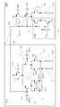
도 1은 삼단 적층 CMOS 전류 모드 로직 계열 래치(CML latch) 회로에 종래 기술에 따른 바이어스 회로를 연결한 상태를 도시한 회로도.1 is a circuit diagram showing a state in which a bias circuit according to the prior art is connected to a three-stage stacked CMOS current mode logic series latch circuit.
도 2는 본 발명 일실시예에 따른 서브 문턱전압 발생기를 적용한 리플리카 바이어스 회로를 도시한 회로도.2 is a circuit diagram illustrating a replica bias circuit to which a sub-threshold voltage generator according to an embodiment of the present invention is applied.
도 3은 도 2의 리플리카 바이어스 회로를 삼단 적층 CMOS 전류 모드 로직 계열 래치 회로에 연결한 상태를 도시한 회로도.3 is a circuit diagram illustrating a state in which the replica bias circuit of FIG. 2 is connected to a three-stage stacked CMOS current mode logic series latch circuit;
도 4는 도 2의 리플리카 바이어스 회로를 삼단 적층 CMOS 전류 모드 로직 계열 AND 회로에 연결한 상태를 도시한 회로도.4 is a circuit diagram showing a state in which the replica bias circuit of FIG. 2 is connected to a three-stage stacked CMOS current mode logic series AND circuit;
* 도면의 주요 부분에 대한 부호의 설명* Explanation of symbols for the main parts of the drawings
110 : 삼단 적층 CMOS 전류 모드 로직 계열 래치 회로110: Three-stage stacked CMOS current mode logic series latch circuit
120 : 레벨 쉬프터 바이어스 회로120: level shifter bias circuit
200 : 리플리카 바이어스 회로200: replica bias circuit
210 : 서브 문턱전압 발생기210: sub threshold voltage generator
410 : 삼단 적층 전류 모드 CMOS 로직 계열 AND 회로410: three-layer stacked current mode CMOS logic series AND circuit
대한민국 특허등록 제 358873호, 래치 회로 및 레지스터 회로Korean Patent Registration No. 358873, Latch Circuit and Register Circuit
미국 특허등록 US6937080호, Current-controlled CMOS logic familyUS patent registration US6937080, Current-controlled CMOS logic family
본 발명은 정전압을 유지하는 바이어스 회로에 관한 것으로, 특히 트랜지스터의 문턱전압 보다 낮은 서브 문턱전압 발생기를 이용한 새로운 리플리카 바이어스로써, 전원 전압이 낮은 응용분야에서도 안정적으로 사용될 수 있는 리플리카 바이어스 회로(replica bias circuit)에 관한 것이다. 예컨대, 직접회로 소자에 널리 사용되는 삼단으로 적층된 CMOS 전류 모드 로직계열(current mode logic : CML) 논리 게이트 및 래치에 바이어스 전압을 공급하는 리플리카 바이어스 회로에 관한 것이다.BACKGROUND OF THE INVENTION 1. Field of the Invention The present invention relates to a bias circuit that maintains a constant voltage, and in particular, as a new replica bias using a sub-threshold voltage generator that is lower than the threshold voltage of a transistor, a replica bias circuit that can be stably used even in a low power supply application. bias circuit). For example, the present invention relates to a replica bias circuit for supplying a bias voltage to a CMOS current mode logic (CML) logic gate and a latch stacked in three stages which are widely used in an integrated circuit device.
일반적인 CMOS 로직계열 회로는 상기 한국 선행특허와 같이 CMOS 스위치(switch)와 CMOS 인버터(inverter) 등으로 구성된다. 이러한 CMOS 로직계열 회로는 안정된 동작을 보이며, 스테틱(static) 전류가 없는 장점이 있는 대신에 속도가 느린 단점이 있다. 따라서, 필요한 동작 속도가 높은 경우에는 상기 미국 선행특허와 같이 CMOS 전류 모드 로직 계열(CML) 을 사용한다. 전류 모드 CMOS 로직 계열은 인버터(inverter) 또는 버퍼 (buffer) 와 같이 이단으로 적층된 구조일 경우도 있지만, 래치(latch) 또는 AND와 같이 삼단으로 적층된 구조일 경우도 있다. 삼단으로 적층된 CMOS 전류 모드 로직 계열(CML)을 사용할 경우 도 1에 도시한 바와 같은 상 기 미국 선행특허에 따른 레벨 쉬프터(level shifter, 120) 등으로 바이어스를 공급하는 경우에는 전원전압과 접지전압간의 차가 충분해야만(예컨대 1.8V 이상) 안정적인 동작을 보장할 수 있다. 그렇지 않을 경우, PVT(process, voltage and temperature) 변화에 민감하게 된다. A general CMOS logic circuit includes a CMOS switch, a CMOS inverter, and the like, as in the Korean patent. Such CMOS logic circuits exhibit stable operation and have a disadvantage of being slow in place of static current. Therefore, when the required operating speed is high, the CMOS current mode logic series (CML) is used as in the US patent. The current mode CMOS logic series may be a two-stacked structure such as an inverter or a buffer, or may be a three-stacked structure such as a latch or an AND. When using a CMOS current mode logic series (CML) stacked in three stages when supplying a bias to a level shifter (120) according to the prior US patent as shown in FIG. Sufficient difference (e.g., 1.8V or more) can ensure stable operation. Otherwise, they are sensitive to changes in process, voltage and temperature (PVT).
그러나, 최근 공정이 발달함에 따라 CMOS 공정은 0.13um 이하, 전원 전압은 1.2V 이하로 낮아지고 있는 상황이다. 따라서, 낮은 전원 전압에서도 삼단으로 적층된 CMOS 전류 모드 로직 계열(CML)을 사용하기 위하여는 이에 적합한 리플리카 바이어스 회로(replica bias circuit)를 구현할 필요가 있다.However, with the recent development of the process, the CMOS process has been lowered to 0.13um or less and the power supply voltage to 1.2V or less. Therefore, in order to use a CMOS current mode logic series (CML) stacked in three stages even at a low power supply voltage, it is necessary to implement a replica bias circuit suitable for this.
상기 문제점들을 해결하기 위하여 안출된 본 발명의 목적은, PVT(process, voltage and temperature) 변화에도 안정적인 바이어스 전압을 유지할 수 있는 리플리카 바이어스 회로를 제공하는데 있다. SUMMARY OF THE INVENTION An object of the present invention devised to solve the above problems is to provide a replica bias circuit capable of maintaining a stable bias voltage even with changes in process, voltage and temperature (PVT).
본 발명의 다른 목적은 전원전압과 접지전압간의 차이가 크지 않은 환경에서도 안정적인 바이어스 전압을 유지할 수 있는 리플리카 바이어스 회로를 제공하는데 있다.Another object of the present invention is to provide a replica bias circuit that can maintain a stable bias voltage even in an environment where the difference between the supply voltage and the ground voltage is not large.
본 발명의 심화된 목적은 고속으로 동작하는 다단으로 적층된 CMOS 전류 모드 로직 계열(CML)을 낮은 전원 전압에서도 안정적으로 사용할 수 있도록 하는 리플리카 바이어스 회로를 제공하는데 있다.It is further an object of the present invention to provide a replica bias circuit that can stably use a multi-layered CMOS current mode logic series (CML) that operates at high speed even at low power supply voltage.
상기 목적을 달성하기 위한 본 발명에 따른 리플리카 바이어스 회로는, 전자회로를 구성하는 타겟 트랜지스터의 게이트에 기준전압을 인가하기 위한 바이어스 회로에 있어서, 트랜지스터 소자의 문턱전압보다 낮은 전압차를 유지시키기 위한 서브 문턱전압 발생기; 및 상기 전자회로 중 상기 타겟 트랜지스터를 포함하는 전류 유동 경로를 이루는 구성 소자들의 규격을 참조하는 소자들을 포함하는 리플리카 경로를 포함하는 것을 특징으로 한다.A replica bias circuit according to the present invention for achieving the above object is a bias circuit for applying a reference voltage to a gate of a target transistor constituting an electronic circuit, for maintaining a voltage difference lower than a threshold voltage of a transistor element; A sub threshold voltage generator; And a replica path including elements referring to specifications of components constituting the current flow path including the target transistor in the electronic circuit.
이하, 본 발명의 바람직한 실시예를 첨부된 도면을 참조하여 상세히 설명한다. 본 실시예는 본 발명의 권리범위를 한정하는 것은 아니고, 단지 예시로 제시된 것이다.Hereinafter, exemplary embodiments of the present invention will be described in detail with reference to the accompanying drawings. This embodiment is not intended to limit the scope of the invention, but is presented by way of example only.
(실시예 1)(Example 1)
도 2는 본 발명에 의한 리플리카 회로(200)의 회로도이며, 도 3은 도 2의 리플리카 바이어스 회로(200)를 삼단 적층 CMOS 전류 모드 로직 계열 래치 회로(110)에 연결한 상태의 회로도이다. 2 is a circuit diagram of a
상기 도면에서, 상기 삼단 적층 CMOS 전류 모드 로직 계열 래치 회로(110)가 본 발명의 사상에 따른 리플리카 회로(200)가 생성한 바이어스 전압을 공급받는 메인 회로가 되며, 상기 삼단 적층 CMOS 전류 모드 로직 계열 래치 회로(110) 중에서도 트랜지스터(112)와 트랜지스터(113)가 직접 상기 바이어스 전압을 공급받는 타겟 소자가 된다.In the figure, the three-stage stacked CMOS current mode logic
상기 도면에 도시한 바와 같이, 바이어스 전압을 공급받는 삼단으로 적층된 CMOS 전류 모드 로직 계열(CML) 래치 회로(110)의 특정한 트랜지스터들(111, 112, 113, 114, 115, 116, 117)의 W/L 크기 또는 저항들 (118, 119)의 저항값들을 참조로 하여 설계된 트랜지스터들(201, 202, 203) 또는 저항 (204)과 서브 문턱전압 발생기(210)로 구성된다. 도 3에서는 리플리카 바이어스 회로(200)를 사용하기 위하여 리플리카 바이어스 회로(200) 와 삼단으로 적층된 전류 모드 로직 래치(110) 사이에 AC 커플링(coupling) 캐패시터(303, 304)와 저항 (301, 302)을 추가하였다.As shown in the figure, the
도시한 구조에서, 트랜지스터(201)는 트랜지스터(111)에 대응되고, 트랜지스터(202)는 트랜지스터(112)에 대응되며, 트랜지스터(203)는 트랜지스터(114)와 트랜지스터(115)에 대응되며, 저항(204)은 저항(118)과 대응된다. 여기서 참조로 하여 설계된다는 것은 다음 식과 같은 관계를 가진다는 의미이다. In the illustrated structure,
즉, 참조로 하여 설계된 경우, 리플리카 경로(220)를 구성하는 각 소자들의 규격(W/L 및 저항값)들의 비가, 바이어스 전압을 공급하는 메인 회로내 대응 경로를 구성하는 각 소자들의 규격들의 비와 동일하다. 또한, 이 때문에, 상기 리플리 카 경로(220)를 구성하는 각 소자들의 규격값은 대응하는 상기 메인 회로내 대응 소자들의 규격값에 동일한 실수n을 곱한값이 된다.That is, when designed with reference, the ratio of the specifications (W / L and resistance values) of the respective elements constituting the
구체적으로 예를 들어 상기 n이 1이라고 하면, 트랜지스터(201)의 W/L은 트랜지스터(111)의 W/L의 1/2 크기와 같다. 트랜지스터(202)의 W/L은 트랜지스터(112)의 W/L과 같다. 트랜지스터(203)의 W/L은 트랜지스터(114)와 트랜지스터(115)의 W/L의 합과 같다.Specifically, for example, when n is 1, the W / L of the
그런데, 트랜지스터(201)는 트랜지스터(111)의 1/2배에 대응하는데, 이는 실제 도 3의 삼단 적층 CMOS 전류 모드 로직 계열 래치 회로에서 트랜지스터(111)의 채널에는 트랜지스터(112)를 경유한 전류와 트랜지스터(113)을 경유한 전류가 동시에 흐르며, 트랜지스터(112)를 경유한 전류와 트랜지스터(113)를 경유한 전류는 그 크기가 거의 동일하여, 그 결과 트랜지스터(112)를 포함하는 전류 유동 경로에서는 트랜지스터(111)은 1/2만이 포함된 것으로 간주되기 때문이다. 또한, 저항(204)의 저항값은 저항(118)의 저항값과 같다. 이과 같은 관계를 가지는 도 2의 바이어스 회로(200)는 도 1의 삼단으로 적층된 전류 모드 로직 래치(110)에 대하여 리플리카(replica) 관계를 가지게 된다.However, the
트랜지스터의 채널 특성과 관련되는 다른 규격들도 상기와 같은 관계를 가질 수 있는데, W/L는 PVT에 민감하며 트랜지스터 채널 성능에 영향이 큰 규격으로서 어떤 경우에도 설계시 반드시 고려하는 것이 바람직하다. Other specifications related to the channel characteristics of the transistor may have the same relationship as above. W / L is a specification that is sensitive to PVT and has a large influence on transistor channel performance.
한편, 상기 서브 문턱전압 발생기(210)는, 저전압 트랜지스터(211); 및 상 기 저전압 트랜지스터에 그 채널 규격에 비해 작은 전류를 흐르도록 하는 서브 문턱전류 강제기를 포함하는데, 상기 서브 문턱전류 강제기는 상기 저전압 트랜지스터(211)와 직렬 연결되며 상기 저전압 트랜지스터(211)의 경우에 비해 작은 크기의 채널 규격(W/L)을 가지는 소전류 트랜지스터(212)로 구현하였다.The
즉, 일반적인 트랜지스터의 문턱전압보다 낮은 전압차를 유지하기 위한 서브 문턱전압 발생기(210)는 서로 매우 상이한 규격(W/L)을 가지는 2개의 트랜지스터(211, 212)로 구현할 수 있다. 이 중 트랜지스터(211)의 W/L은 트랜지스터(202) 의 W/L과 같은 크기로 구현할 수 있다. 트랜지스터(212)는 트랜지스터(211)에 비해 W/L 이 매우 작은 트랜지스터이다. 트랜지스터(212)의 W/L 을 매우 작게 설계함으로써, 트랜지스터(211)의 채널을 통해 흐르는 전류를 트랜지스터(211)의 문턱 전류보다 작게 하고, 최종적으로 트랜지스터(211)의 Vgs(gate source 전압)를 문턱 전압보다 작게 할 수 있다. 리플리카 바이어스 회로(200)의 각 트랜지스터의 연결을 도 2와 같이 함으로써, 트랜지스터(202)의 Vgd(gate drain 전압)는 트랜지스터(211)의 Vgs (gate source 전압)과 같아진다. 따라서, 트랜지스터(211)의 Vgs과 트랜지스터(202)의 Vgd는 문턱전압보다 작아지고, 트랜지스터(202)는 언제나 안정적으로 세츄레이션(saturation) 영역에서 동작하게 된다.That is, the
여기서, 상기와 같이 세츄레이션 영역으로 동작하는 트랜지스터(202)는 PVT에 민감해질 가능성이 높다. 그러나, 상기 트랜지스터(202)는 리플리카 경로(220)를 형성하며, 상기 리플리카 경로(220)는 바이어스 전압을 공급받는 메인 회로의 전류 유동 경로와 동일한 규격비의 소자들로 이루어져 있으므로, 상기 리플리카 경 로와 메인 회로를 동일한 공정에서 제조하였을 경우, PVT변화에 의한 트랜지스터(202)의 특성 변화 효과는, 동일한 PVT 변화에 의한 상기 메인 회로의 특성 변화에 의해 상쇄된다.Here, the
이러한 방식으로 트랜지스터(202)의 게이트(gate) 전압을 필요 이상으로 크게 하지 않으면서도, 낮은 전원 전압에서 안정적인 동작을 보장할 수 있게 된다.In this manner, stable operation can be ensured at a low power supply voltage without making the gate voltage of the
(실시예 2)(Example 2)
도 4는 도 2의 서브 문턱전압 발생기(210)를 이용한 리플리카 바이어스 회로 (200)를 삼단으로 적층된 전류 모드 CMOS 로직 계열 AND(CML AND, 410)에 적용한 회로도이다. 리플리카 바이어스 회로(200)를 사용하기 위하여 리플리카 바이어스 회로(200)와 삼단으로 적층된 전류 모드 로직 AND(410) 사이에 AC 커플링 캐패시터 (403, 404)와 저항(401, 402)을 추가하였다.4 is a circuit diagram of a
상기 도면에서, 상기 삼단 적층 CMOS 전류 모드 로직 계열 AND 회로(410)가 본 발명의 사상에 따른 리플리카 회로(200)가 생성한 바이어스 전압을 공급받는 메인 회로가 되며, 상기 삼단 적층 CMOS 전류 모드 로직 계열 AND 회로(410) 중에서도 트랜지스터(412)와 트랜지스터(413)가 직접 상기 바이어스 전압을 공급받는 타겟 소자가 된다.In the figure, the three-stage stacked CMOS current mode logic series AND
삼단으로 적층된 전류 모드 CMOS 로직 계열 래치 회로가, 삼단으로 적층된 전류 모드 CMOS 로직 계열 AND회로로 대치되면서, 트랜지스터(116, 117)의 연결구조와 트랜지스터(416, 417)의 연결구조가 변경된 차이가 있으나, 이 차이는 본 발 명의 사상을 구현하는데 무관하며, 다른 구조는 상기 제1 실시예의 경우와 거의 동일하므로 자세한 설명을 생략한다.The difference between the connection structure of the
상기한 바와 같은 본 발명에 의한 리플리카 바이어스 회로를 제공함에 따라, 다단으로 적층된 CMOS 전류 모드 로직 계열(CML) 회로들이 낮은 전원 전압에서도 안정적으로 동작하는 효과가 있다.By providing a replica bias circuit according to the present invention as described above, there is an effect that the multi-layer stacked CMOS current mode logic series (CML) circuits operate stably even at a low power supply voltage.
또한, 본 발명에 의한 리플리카 바이어스 회로는 PVT(process, voltage and temperature) 변화에도 안정적인 바이어스 전압을 유지할 수 있는 효과도 있다. In addition, the replica bias circuit according to the present invention has the effect of maintaining a stable bias voltage even in the process, voltage and temperature (PVT) changes.
또한, 본 발명에 의한 리플리카 바이어스 회로는 전원전압과 접지전압간의 차이가 크지 않은 환경에서도 안정적인 바이어스 전압을 유지할 수 있는 효과도 있다.In addition, the replica bias circuit according to the present invention has the effect of maintaining a stable bias voltage even in an environment where the difference between the power supply voltage and the ground voltage is not large.
또한, 본 발명에 의한 리플리카 바이어스 회로는 고속으로 동작하는 다단으로 적층된 CMOS 전류 모드 로직 계열(CML)을 낮은 전원 전압에서도 안정적으로 사용하게 하는 효과도 있다.In addition, the replica bias circuit according to the present invention has an effect of stably using a multi-stage CMOS current mode logic series (CML) that operates at high speed even at a low power supply voltage.
Claims (8)
Priority Applications (2)
| Application Number | Priority Date | Filing Date | Title |
|---|---|---|---|
| KR1020050109054A KR100631049B1 (en) | 2005-11-15 | 2005-11-15 | Replica bias circuit |
| US11/451,962 US7429874B2 (en) | 2005-11-15 | 2006-06-13 | Replica bias circuit |
Applications Claiming Priority (1)
| Application Number | Priority Date | Filing Date | Title |
|---|---|---|---|
| KR1020050109054A KR100631049B1 (en) | 2005-11-15 | 2005-11-15 | Replica bias circuit |
Publications (1)
| Publication Number | Publication Date |
|---|---|
| KR100631049B1 true KR100631049B1 (en) | 2006-10-04 |
Family
ID=37622804
Family Applications (1)
| Application Number | Title | Priority Date | Filing Date |
|---|---|---|---|
| KR1020050109054A Expired - Fee Related KR100631049B1 (en) | 2005-11-15 | 2005-11-15 | Replica bias circuit |
Country Status (2)
| Country | Link |
|---|---|
| US (1) | US7429874B2 (en) |
| KR (1) | KR100631049B1 (en) |
Cited By (1)
| Publication number | Priority date | Publication date | Assignee | Title |
|---|---|---|---|---|
| US8228709B2 (en) | 2008-11-04 | 2012-07-24 | Samsung Electronics Co., Ltd. | Resistance variable memory device and system |
Families Citing this family (8)
| Publication number | Priority date | Publication date | Assignee | Title |
|---|---|---|---|---|
| DE102006010978B4 (en) * | 2006-03-09 | 2015-01-22 | Austriamicrosystems Ag | Oscillator arrangement and method for operating a quartz crystal |
| TWI350646B (en) * | 2007-06-05 | 2011-10-11 | O2Micro Int Ltd | Frequency divider and latch circuit and frequency dividing method thereof |
| TW200904002A (en) * | 2007-07-03 | 2009-01-16 | Toppoly Optoelectronics Corp | Level shifter, interface driving circuit, and image display system |
| JP5176971B2 (en) * | 2009-01-15 | 2013-04-03 | 富士通株式会社 | DC potential generation circuit, multistage circuit, and communication device |
| CN102075179B (en) * | 2010-12-31 | 2012-08-22 | 东南大学 | A subthreshold latch |
| US8803551B2 (en) | 2012-07-30 | 2014-08-12 | Infineon Technologies Austria Ag | Low supply voltage logic circuit |
| US10644699B2 (en) | 2018-05-31 | 2020-05-05 | Texas Instruments Incorporated | Lower voltage switching of current mode logic circuits |
| US10566957B1 (en) | 2019-04-08 | 2020-02-18 | Semiconductor Components Industries, Llc | Current-mode logic latches for a PVT-robust mod 3 frequency divider |
Citations (2)
| Publication number | Priority date | Publication date | Assignee | Title |
|---|---|---|---|---|
| JP2001320243A (en) | 2000-05-12 | 2001-11-16 | Sony Corp | Bias circuit and wireless communication device using the same |
| JP2001326560A (en) | 2000-05-18 | 2001-11-22 | Toshiba Corp | Semiconductor integrated circuit and phase locked loop circuit |
Family Cites Families (9)
| Publication number | Priority date | Publication date | Assignee | Title |
|---|---|---|---|---|
| US5798658A (en) * | 1995-06-15 | 1998-08-25 | Werking; Paul M. | Source-coupled logic with reference controlled inputs |
| US5541532A (en) * | 1995-08-17 | 1996-07-30 | Analog Devices, Inc. | All MOS single-ended to differential level converter |
| US6094074A (en) * | 1998-07-16 | 2000-07-25 | Seiko Epson Corporation | High speed common mode logic circuit |
| JP3530422B2 (en) | 1999-06-16 | 2004-05-24 | Necエレクトロニクス株式会社 | Latch circuit and register circuit |
| US6081162A (en) * | 1999-06-17 | 2000-06-27 | Intel Corporation | Robust method and apparatus for providing a digital single-ended output from a differential input |
| US6424194B1 (en) * | 1999-06-28 | 2002-07-23 | Broadcom Corporation | Current-controlled CMOS logic family |
| US6380797B1 (en) * | 2000-10-25 | 2002-04-30 | National Semiconductor Corporation | High speed low voltage differential signal driver circuit having low sensitivity to fabrication process variation, noise, and operating temperature variation |
| KR100423011B1 (en) | 2001-09-29 | 2004-03-16 | 주식회사 버카나와이어리스코리아 | Charge Pump Circuit for PLL |
| US6762624B2 (en) | 2002-09-03 | 2004-07-13 | Agilent Technologies, Inc. | Current mode logic family with bias current compensation |
-
2005
- 2005-11-15 KR KR1020050109054A patent/KR100631049B1/en not_active Expired - Fee Related
-
2006
- 2006-06-13 US US11/451,962 patent/US7429874B2/en not_active Expired - Fee Related
Patent Citations (2)
| Publication number | Priority date | Publication date | Assignee | Title |
|---|---|---|---|---|
| JP2001320243A (en) | 2000-05-12 | 2001-11-16 | Sony Corp | Bias circuit and wireless communication device using the same |
| JP2001326560A (en) | 2000-05-18 | 2001-11-22 | Toshiba Corp | Semiconductor integrated circuit and phase locked loop circuit |
Cited By (1)
| Publication number | Priority date | Publication date | Assignee | Title |
|---|---|---|---|---|
| US8228709B2 (en) | 2008-11-04 | 2012-07-24 | Samsung Electronics Co., Ltd. | Resistance variable memory device and system |
Also Published As
| Publication number | Publication date |
|---|---|
| US20070120600A1 (en) | 2007-05-31 |
| US7429874B2 (en) | 2008-09-30 |
Similar Documents
| Publication | Publication Date | Title |
|---|---|---|
| US7683667B2 (en) | Level shifter having single voltage source | |
| JP5430507B2 (en) | Voltage level shifter | |
| US7468615B1 (en) | Voltage level shifter | |
| US10200043B2 (en) | Level shifter | |
| US7397297B2 (en) | Level shifter circuit | |
| US12081215B2 (en) | Level shifter circuit and method of operating the same | |
| KR100631049B1 (en) | Replica bias circuit | |
| WO2017048550A1 (en) | Level shifter applicable to low voltage domain to high voltage domain conversion | |
| US7605636B2 (en) | Power gating structure, semiconductor including the same and method of controlling a power gating | |
| US10291230B2 (en) | Level shifter and level shifting method | |
| US7456662B2 (en) | Differential circuit, output buffer circuit and semiconductor integrated circuit for a multi-power system | |
| US9979399B2 (en) | Level shifter | |
| US7498842B2 (en) | High speed voltage level shifter circuits | |
| JP2005286683A (en) | Data output circuit | |
| US6417716B1 (en) | CMOS voltage shifter | |
| US7133487B2 (en) | Level shifter | |
| US9608604B2 (en) | Voltage level shifter with single well voltage | |
| US6407590B2 (en) | High frequency differential receiver | |
| US20080084231A1 (en) | Method for Implementing Level Shifter Circuits and Low Power Level Shifter Circuits for Integrated Circuits | |
| US7362137B2 (en) | High speed voltage level shifter circuits | |
| US20090184696A1 (en) | Voltage source for gate oxide protection | |
| CN108628379B (en) | Bias circuit | |
| JP2006135712A (en) | Level shifter circuit and semiconductor integrated circuit having the same | |
| KR20040095886A (en) | Bootstrap Circuit | |
| WO2006103624A1 (en) | Electronic device |
Legal Events
| Date | Code | Title | Description |
|---|---|---|---|
| A201 | Request for examination | ||
| PA0109 | Patent application |
St.27 status event code: A-0-1-A10-A12-nap-PA0109 |
|
| PA0201 | Request for examination |
St.27 status event code: A-1-2-D10-D11-exm-PA0201 |
|
| D13-X000 | Search requested |
St.27 status event code: A-1-2-D10-D13-srh-X000 |
|
| D14-X000 | Search report completed |
St.27 status event code: A-1-2-D10-D14-srh-X000 |
|
| E701 | Decision to grant or registration of patent right | ||
| PE0701 | Decision of registration |
St.27 status event code: A-1-2-D10-D22-exm-PE0701 |
|
| GRNT | Written decision to grant | ||
| PR0701 | Registration of establishment |
St.27 status event code: A-2-4-F10-F11-exm-PR0701 |
|
| PR1002 | Payment of registration fee |
St.27 status event code: A-2-2-U10-U11-oth-PR1002 Fee payment year number: 1 |
|
| PG1601 | Publication of registration |
St.27 status event code: A-4-4-Q10-Q13-nap-PG1601 |
|
| PN2301 | Change of applicant |
St.27 status event code: A-5-5-R10-R13-asn-PN2301 St.27 status event code: A-5-5-R10-R11-asn-PN2301 |
|
| PR1001 | Payment of annual fee |
St.27 status event code: A-4-4-U10-U11-oth-PR1001 Fee payment year number: 4 |
|
| PR1001 | Payment of annual fee |
St.27 status event code: A-4-4-U10-U11-oth-PR1001 Fee payment year number: 5 |
|
| PR1001 | Payment of annual fee |
St.27 status event code: A-4-4-U10-U11-oth-PR1001 Fee payment year number: 6 |
|
| FPAY | Annual fee payment |
Payment date: 20120910 Year of fee payment: 7 |
|
| PR1001 | Payment of annual fee |
St.27 status event code: A-4-4-U10-U11-oth-PR1001 Fee payment year number: 7 |
|
| FPAY | Annual fee payment |
Payment date: 20130829 Year of fee payment: 8 |
|
| PR1001 | Payment of annual fee |
St.27 status event code: A-4-4-U10-U11-oth-PR1001 Fee payment year number: 8 |
|
| FPAY | Annual fee payment |
Payment date: 20140827 Year of fee payment: 9 |
|
| PR1001 | Payment of annual fee |
St.27 status event code: A-4-4-U10-U11-oth-PR1001 Fee payment year number: 9 |
|
| PN2301 | Change of applicant |
St.27 status event code: A-5-5-R10-R13-asn-PN2301 St.27 status event code: A-5-5-R10-R11-asn-PN2301 |
|
| FPAY | Annual fee payment |
Payment date: 20150827 Year of fee payment: 10 |
|
| PR1001 | Payment of annual fee |
St.27 status event code: A-4-4-U10-U11-oth-PR1001 Fee payment year number: 10 |
|
| FPAY | Annual fee payment |
Payment date: 20160826 Year of fee payment: 11 |
|
| PR1001 | Payment of annual fee |
St.27 status event code: A-4-4-U10-U11-oth-PR1001 Fee payment year number: 11 |
|
| FPAY | Annual fee payment |
Payment date: 20170828 Year of fee payment: 12 |
|
| PR1001 | Payment of annual fee |
St.27 status event code: A-4-4-U10-U11-oth-PR1001 Fee payment year number: 12 |
|
| PR1001 | Payment of annual fee |
St.27 status event code: A-4-4-U10-U11-oth-PR1001 Fee payment year number: 13 |
|
| PC1903 | Unpaid annual fee |
St.27 status event code: A-4-4-U10-U13-oth-PC1903 Not in force date: 20190927 Payment event data comment text: Termination Category : DEFAULT_OF_REGISTRATION_FEE |
|
| PC1903 | Unpaid annual fee |
St.27 status event code: N-4-6-H10-H13-oth-PC1903 Ip right cessation event data comment text: Termination Category : DEFAULT_OF_REGISTRATION_FEE Not in force date: 20190927 |