JP6453195B2 - 車載制御装置 - Google Patents
車載制御装置 Download PDFInfo
- Publication number
- JP6453195B2 JP6453195B2 JP2015190611A JP2015190611A JP6453195B2 JP 6453195 B2 JP6453195 B2 JP 6453195B2 JP 2015190611 A JP2015190611 A JP 2015190611A JP 2015190611 A JP2015190611 A JP 2015190611A JP 6453195 B2 JP6453195 B2 JP 6453195B2
- Authority
- JP
- Japan
- Prior art keywords
- heat
- circuit board
- electronic component
- resin
- vehicle
- Prior art date
- Legal status (The legal status is an assumption and is not a legal conclusion. Google has not performed a legal analysis and makes no representation as to the accuracy of the status listed.)
- Active
Links
Images


Classifications
-
- H—ELECTRICITY
- H10—SEMICONDUCTOR DEVICES; ELECTRIC SOLID-STATE DEVICES NOT OTHERWISE PROVIDED FOR
- H10W—GENERIC PACKAGES, INTERCONNECTIONS, CONNECTORS OR OTHER CONSTRUCTIONAL DETAILS OF DEVICES COVERED BY CLASS H10
- H10W40/00—Arrangements for thermal protection or thermal control
- H10W40/20—Arrangements for cooling
- H10W40/22—Arrangements for cooling characterised by their shape, e.g. having conical or cylindrical projections
-
- H—ELECTRICITY
- H05—ELECTRIC TECHNIQUES NOT OTHERWISE PROVIDED FOR
- H05K—PRINTED CIRCUITS; CASINGS OR CONSTRUCTIONAL DETAILS OF ELECTRIC APPARATUS; MANUFACTURE OF ASSEMBLAGES OF ELECTRICAL COMPONENTS
- H05K5/00—Casings, cabinets or drawers for electric apparatus
- H05K5/0026—Casings, cabinets or drawers for electric apparatus provided with connectors and printed circuit boards [PCB], e.g. automotive electronic control units
- H05K5/0034—Casings, cabinets or drawers for electric apparatus provided with connectors and printed circuit boards [PCB], e.g. automotive electronic control units having an overmolded housing covering the PCB
-
- B—PERFORMING OPERATIONS; TRANSPORTING
- B29—WORKING OF PLASTICS; WORKING OF SUBSTANCES IN A PLASTIC STATE IN GENERAL
- B29C—SHAPING OR JOINING OF PLASTICS; SHAPING OF MATERIAL IN A PLASTIC STATE, NOT OTHERWISE PROVIDED FOR; AFTER-TREATMENT OF THE SHAPED PRODUCTS, e.g. REPAIRING
- B29C45/00—Injection moulding, i.e. forcing the required volume of moulding material through a nozzle into a closed mould; Apparatus therefor
- B29C45/14—Injection moulding, i.e. forcing the required volume of moulding material through a nozzle into a closed mould; Apparatus therefor incorporating preformed parts or layers, e.g. injection moulding around inserts or for coating articles
- B29C45/14836—Preventing damage of inserts during injection, e.g. collapse of hollow inserts, breakage
-
- B—PERFORMING OPERATIONS; TRANSPORTING
- B60—VEHICLES IN GENERAL
- B60R—VEHICLES, VEHICLE FITTINGS, OR VEHICLE PARTS, NOT OTHERWISE PROVIDED FOR
- B60R16/00—Electric or fluid circuits specially adapted for vehicles and not otherwise provided for; Arrangement of elements of electric or fluid circuits specially adapted for vehicles and not otherwise provided for
- B60R16/02—Electric or fluid circuits specially adapted for vehicles and not otherwise provided for; Arrangement of elements of electric or fluid circuits specially adapted for vehicles and not otherwise provided for electric constitutive elements
- B60R16/023—Electric or fluid circuits specially adapted for vehicles and not otherwise provided for; Arrangement of elements of electric or fluid circuits specially adapted for vehicles and not otherwise provided for electric constitutive elements for transmission of signals between vehicle parts or subsystems
- B60R16/0231—Circuits relating to the driving or the functioning of the vehicle
-
- H—ELECTRICITY
- H05—ELECTRIC TECHNIQUES NOT OTHERWISE PROVIDED FOR
- H05K—PRINTED CIRCUITS; CASINGS OR CONSTRUCTIONAL DETAILS OF ELECTRIC APPARATUS; MANUFACTURE OF ASSEMBLAGES OF ELECTRICAL COMPONENTS
- H05K1/00—Printed circuits
- H05K1/02—Details
- H05K1/0201—Thermal arrangements, e.g. for cooling, heating or preventing overheating
- H05K1/0203—Cooling of mounted components
-
- H—ELECTRICITY
- H05—ELECTRIC TECHNIQUES NOT OTHERWISE PROVIDED FOR
- H05K—PRINTED CIRCUITS; CASINGS OR CONSTRUCTIONAL DETAILS OF ELECTRIC APPARATUS; MANUFACTURE OF ASSEMBLAGES OF ELECTRICAL COMPONENTS
- H05K5/00—Casings, cabinets or drawers for electric apparatus
- H05K5/0026—Casings, cabinets or drawers for electric apparatus provided with connectors and printed circuit boards [PCB], e.g. automotive electronic control units
- H05K5/0082—Casings, cabinets or drawers for electric apparatus provided with connectors and printed circuit boards [PCB], e.g. automotive electronic control units specially adapted for transmission control units, e.g. gearbox controllers
-
- H—ELECTRICITY
- H05—ELECTRIC TECHNIQUES NOT OTHERWISE PROVIDED FOR
- H05K—PRINTED CIRCUITS; CASINGS OR CONSTRUCTIONAL DETAILS OF ELECTRIC APPARATUS; MANUFACTURE OF ASSEMBLAGES OF ELECTRICAL COMPONENTS
- H05K7/00—Constructional details common to different types of electric apparatus
- H05K7/20—Modifications to facilitate cooling, ventilating, or heating
- H05K7/2039—Modifications to facilitate cooling, ventilating, or heating characterised by the heat transfer by conduction from the heat generating element to a dissipating body
- H05K7/20436—Inner thermal coupling elements in heat dissipating housings, e.g. protrusions or depressions integrally formed in the housing
- H05K7/20445—Inner thermal coupling elements in heat dissipating housings, e.g. protrusions or depressions integrally formed in the housing the coupling element being an additional piece, e.g. thermal standoff
- H05K7/20454—Inner thermal coupling elements in heat dissipating housings, e.g. protrusions or depressions integrally formed in the housing the coupling element being an additional piece, e.g. thermal standoff with a conformable or flexible structure compensating for irregularities, e.g. cushion bags, thermal paste
-
- H—ELECTRICITY
- H05—ELECTRIC TECHNIQUES NOT OTHERWISE PROVIDED FOR
- H05K—PRINTED CIRCUITS; CASINGS OR CONSTRUCTIONAL DETAILS OF ELECTRIC APPARATUS; MANUFACTURE OF ASSEMBLAGES OF ELECTRICAL COMPONENTS
- H05K7/00—Constructional details common to different types of electric apparatus
- H05K7/20—Modifications to facilitate cooling, ventilating, or heating
- H05K7/2039—Modifications to facilitate cooling, ventilating, or heating characterised by the heat transfer by conduction from the heat generating element to a dissipating body
- H05K7/20436—Inner thermal coupling elements in heat dissipating housings, e.g. protrusions or depressions integrally formed in the housing
- H05K7/20445—Inner thermal coupling elements in heat dissipating housings, e.g. protrusions or depressions integrally formed in the housing the coupling element being an additional piece, e.g. thermal standoff
- H05K7/20463—Filling compound, e.g. potted resin
-
- H—ELECTRICITY
- H05—ELECTRIC TECHNIQUES NOT OTHERWISE PROVIDED FOR
- H05K—PRINTED CIRCUITS; CASINGS OR CONSTRUCTIONAL DETAILS OF ELECTRIC APPARATUS; MANUFACTURE OF ASSEMBLAGES OF ELECTRICAL COMPONENTS
- H05K7/00—Constructional details common to different types of electric apparatus
- H05K7/20—Modifications to facilitate cooling, ventilating, or heating
- H05K7/20845—Modifications to facilitate cooling, ventilating, or heating for automotive electronic casings
- H05K7/20854—Heat transfer by conduction from internal heat source to heat radiating structure
-
- H—ELECTRICITY
- H05—ELECTRIC TECHNIQUES NOT OTHERWISE PROVIDED FOR
- H05K—PRINTED CIRCUITS; CASINGS OR CONSTRUCTIONAL DETAILS OF ELECTRIC APPARATUS; MANUFACTURE OF ASSEMBLAGES OF ELECTRICAL COMPONENTS
- H05K7/00—Constructional details common to different types of electric apparatus
- H05K7/20—Modifications to facilitate cooling, ventilating, or heating
- H05K7/2089—Modifications to facilitate cooling, ventilating, or heating for power electronics, e.g. for inverters for controlling motor
- H05K7/209—Heat transfer by conduction from internal heat source to heat radiating structure
-
- H—ELECTRICITY
- H10—SEMICONDUCTOR DEVICES; ELECTRIC SOLID-STATE DEVICES NOT OTHERWISE PROVIDED FOR
- H10W—GENERIC PACKAGES, INTERCONNECTIONS, CONNECTORS OR OTHER CONSTRUCTIONAL DETAILS OF DEVICES COVERED BY CLASS H10
- H10W40/00—Arrangements for thermal protection or thermal control
- H10W40/10—Arrangements for heating
-
- H—ELECTRICITY
- H10—SEMICONDUCTOR DEVICES; ELECTRIC SOLID-STATE DEVICES NOT OTHERWISE PROVIDED FOR
- H10W—GENERIC PACKAGES, INTERCONNECTIONS, CONNECTORS OR OTHER CONSTRUCTIONAL DETAILS OF DEVICES COVERED BY CLASS H10
- H10W40/00—Arrangements for thermal protection or thermal control
- H10W40/20—Arrangements for cooling
- H10W40/25—Arrangements for cooling characterised by their materials
- H10W40/258—Metallic materials
-
- H—ELECTRICITY
- H10—SEMICONDUCTOR DEVICES; ELECTRIC SOLID-STATE DEVICES NOT OTHERWISE PROVIDED FOR
- H10W—GENERIC PACKAGES, INTERCONNECTIONS, CONNECTORS OR OTHER CONSTRUCTIONAL DETAILS OF DEVICES COVERED BY CLASS H10
- H10W74/00—Encapsulations, e.g. protective coatings
-
- H—ELECTRICITY
- H10—SEMICONDUCTOR DEVICES; ELECTRIC SOLID-STATE DEVICES NOT OTHERWISE PROVIDED FOR
- H10W—GENERIC PACKAGES, INTERCONNECTIONS, CONNECTORS OR OTHER CONSTRUCTIONAL DETAILS OF DEVICES COVERED BY CLASS H10
- H10W74/00—Encapsulations, e.g. protective coatings
- H10W74/01—Manufacture or treatment
- H10W74/016—Manufacture or treatment using moulds
-
- H—ELECTRICITY
- H10—SEMICONDUCTOR DEVICES; ELECTRIC SOLID-STATE DEVICES NOT OTHERWISE PROVIDED FOR
- H10W—GENERIC PACKAGES, INTERCONNECTIONS, CONNECTORS OR OTHER CONSTRUCTIONAL DETAILS OF DEVICES COVERED BY CLASS H10
- H10W74/00—Encapsulations, e.g. protective coatings
- H10W74/10—Encapsulations, e.g. protective coatings characterised by their shape or disposition
- H10W74/111—Encapsulations, e.g. protective coatings characterised by their shape or disposition the semiconductor body being completely enclosed
- H10W74/114—Encapsulations, e.g. protective coatings characterised by their shape or disposition the semiconductor body being completely enclosed by a substrate and the encapsulations
-
- H—ELECTRICITY
- H10—SEMICONDUCTOR DEVICES; ELECTRIC SOLID-STATE DEVICES NOT OTHERWISE PROVIDED FOR
- H10W—GENERIC PACKAGES, INTERCONNECTIONS, CONNECTORS OR OTHER CONSTRUCTIONAL DETAILS OF DEVICES COVERED BY CLASS H10
- H10W76/00—Containers; Fillings or auxiliary members therefor; Seals
- H10W76/10—Containers or parts thereof
- H10W76/12—Containers or parts thereof characterised by their shape
-
- H—ELECTRICITY
- H10—SEMICONDUCTOR DEVICES; ELECTRIC SOLID-STATE DEVICES NOT OTHERWISE PROVIDED FOR
- H10W—GENERIC PACKAGES, INTERCONNECTIONS, CONNECTORS OR OTHER CONSTRUCTIONAL DETAILS OF DEVICES COVERED BY CLASS H10
- H10W90/00—Package configurations
-
- B—PERFORMING OPERATIONS; TRANSPORTING
- B29—WORKING OF PLASTICS; WORKING OF SUBSTANCES IN A PLASTIC STATE IN GENERAL
- B29C—SHAPING OR JOINING OF PLASTICS; SHAPING OF MATERIAL IN A PLASTIC STATE, NOT OTHERWISE PROVIDED FOR; AFTER-TREATMENT OF THE SHAPED PRODUCTS, e.g. REPAIRING
- B29C45/00—Injection moulding, i.e. forcing the required volume of moulding material through a nozzle into a closed mould; Apparatus therefor
- B29C45/0046—Details relating to the filling pattern or flow paths or flow characteristics of moulding material in the mould cavity
- B29C2045/0049—Details relating to the filling pattern or flow paths or flow characteristics of moulding material in the mould cavity the injected material flowing against a mould cavity protruding part
-
- H—ELECTRICITY
- H10—SEMICONDUCTOR DEVICES; ELECTRIC SOLID-STATE DEVICES NOT OTHERWISE PROVIDED FOR
- H10W—GENERIC PACKAGES, INTERCONNECTIONS, CONNECTORS OR OTHER CONSTRUCTIONAL DETAILS OF DEVICES COVERED BY CLASS H10
- H10W90/00—Package configurations
- H10W90/701—Package configurations characterised by the relative positions of pads or connectors relative to package parts
- H10W90/731—Package configurations characterised by the relative positions of pads or connectors relative to package parts of die-attach connectors
- H10W90/736—Package configurations characterised by the relative positions of pads or connectors relative to package parts of die-attach connectors between a chip and a stacked lead frame, conducting package substrate or heat sink
Landscapes
- Engineering & Computer Science (AREA)
- Microelectronics & Electronic Packaging (AREA)
- Physics & Mathematics (AREA)
- Thermal Sciences (AREA)
- Mechanical Engineering (AREA)
- Automation & Control Theory (AREA)
- Manufacturing & Machinery (AREA)
- Cooling Or The Like Of Electrical Apparatus (AREA)
- Cooling Or The Like Of Semiconductors Or Solid State Devices (AREA)
- Chemical & Material Sciences (AREA)
- Materials Engineering (AREA)
- Structures Or Materials For Encapsulating Or Coating Semiconductor Devices Or Solid State Devices (AREA)
Description
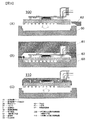
図1は、本発明の第1の実施形態である車載制御装置の断面図である。図1の発熱電子部品周りの局所構造を抽出したのが図4である。本発明に係る構成として、図4の(A)、(B)、(C)が可能である。図4(A)は、放熱金属ベース10の発熱電子部品42下部に相当する領域に凹み部を設け、ここに放熱材50を配置した構成である。図4(B)は、図4(A)の凹み部周囲に突起部を設けた構成である。図4(C)は、図4(B)の凹み部を無くし、突起部を残したものである。
本実施例は、第一の実施形態の放熱金属ベース突起部を図10(B)(C)(D)の形状にした場合である。放熱金属ベース突起部の高さは、図6に示すように各種のものが適用可能であり、それぞれで期待できる効果の内容に違いが生じる。図6(A)では第一の実施形態で記載した効果があり、図6(B)が本実施例の場合である。図6(B)の構成で樹脂封止した場合の実施形態である車載制御装置の断面図を図2に示す。突起部高さが高いため放熱材50を多く充填可能で、放熱材50を発熱電子部品リード部も覆うように配置できるため、放熱効果を一層高めることが可能である。
本実施例は、第一の実施形態の放熱金属ベース突起部を図11(B−1)の形状にした場合である。放熱金属ベース突起部の高さは、図6に示すように各種のものが適用可能であり、それぞれで期待できる効果に違いが生じる。図6(A)では第一の実施形態で記載した、放熱材節約・保護の効果があり、図6(B)では第二の実施形態で記載した、放熱材節約・保護に加え、狭い隙間への樹脂充填性確保の効果があり、図6(C)が本実施例の場合である。
本実施例は、放熱金属ベースの突起部を放熱ベースと別部材にしたものである。上記第一〜第三の実施例の何れにも適用可能である。突起部の材質としては、放熱金属ベースと同じ材料、別の金属材料、樹脂材料、ガラスやセラミックスなど無機材料などから選択することができる。予め上記材料で突起構造体を形成し、これを放熱金属ベースの該当する位置に固定する。固定手段としては、接着、溶着、摩擦接合など含め、適宜手法を選択する。また、ペースト状の材料をディスペンス手法などで放熱金属ベースの所定の位置に突起形状を形成してから硬化あるいは固化させてもよい。
Claims (5)
- 回路基板と、
前記回路基板に対向して設けられる部材と、
前記回路基板上の前記部材側に実装される発熱電子部品と、
前記発熱電子部品と前記部材との間に設けられた放熱材と、
前記回路基板と前記発熱電子部品とを封止する封止樹脂と、を備え、
前記部材は、前記放熱材が設けられていない範囲の少なくとも一部に、前記回路基板側に突出した突出部を備え、
前記突出部は、少なくとも3箇所で前記回路基板に接触し、
前記突出部により、前記部材と前記回路基板との間の間隔が、前記放熱材が設けられていない範囲の少なくとも一部で、前記放熱材が設けられている範囲よりも狭いことを特徴とする車載制御装置。 - 回路基板と、
前記回路基板に対向して設けられる部材と、
前記回路基板上の前記部材側に実装される発熱電子部品と、
前記発熱電子部品と前記部材との間に設けられた放熱材と、
前記回路基板と前記発熱電子部品とを封止する封止樹脂と、を備え、
前記部材は、前記放熱材が設けられていない範囲の少なくとも一部に、前記回路基板側に突出した突出部を備え、
前記突出部は、前記部材とは別部材で構成され
前記突出部により、前記部材と前記回路基板との間の間隔が、前記放熱材が設けられていない範囲の少なくとも一部で、前記放熱材が設けられている範囲よりも狭いことを特徴とする車載制御装置。 - 請求項1または2記載の車載制御装置において、
前記突出部は、前記発熱電子部品を囲むように切れ目の無い形状であることを特徴とする車載制御装置。 - 請求項1から3いずれか一項記載の車載制御装置において、
前記突出部は、前記部材と前記発熱電子部品との間隔より長く前記回路基板側に突出していることを特徴とする車載制御装置。 - 請求項1から4いずれか一項記載の車載制御装置において、
前記放熱材は、熱伝導性樹脂、熱伝導性接着剤、熱伝導性グリース、熱伝導性ゲルの何れかから選択された材料であることを特徴とする車載制御装置。
Priority Applications (5)
| Application Number | Priority Date | Filing Date | Title |
|---|---|---|---|
| JP2015190611A JP6453195B2 (ja) | 2015-09-29 | 2015-09-29 | 車載制御装置 |
| US15/763,380 US10396010B2 (en) | 2015-09-29 | 2016-08-08 | Onboard control device |
| CN201680046296.8A CN107926134A (zh) | 2015-09-29 | 2016-08-08 | 车载控制装置 |
| EP16850912.3A EP3358922B1 (en) | 2015-09-29 | 2016-08-08 | Onboard control device |
| PCT/JP2016/073222 WO2017056735A1 (ja) | 2015-09-29 | 2016-08-08 | 車載制御装置 |
Applications Claiming Priority (1)
| Application Number | Priority Date | Filing Date | Title |
|---|---|---|---|
| JP2015190611A JP6453195B2 (ja) | 2015-09-29 | 2015-09-29 | 車載制御装置 |
Publications (2)
| Publication Number | Publication Date |
|---|---|
| JP2017069296A JP2017069296A (ja) | 2017-04-06 |
| JP6453195B2 true JP6453195B2 (ja) | 2019-01-16 |
Family
ID=58424014
Family Applications (1)
| Application Number | Title | Priority Date | Filing Date |
|---|---|---|---|
| JP2015190611A Active JP6453195B2 (ja) | 2015-09-29 | 2015-09-29 | 車載制御装置 |
Country Status (5)
| Country | Link |
|---|---|
| US (1) | US10396010B2 (ja) |
| EP (1) | EP3358922B1 (ja) |
| JP (1) | JP6453195B2 (ja) |
| CN (1) | CN107926134A (ja) |
| WO (1) | WO2017056735A1 (ja) |
Families Citing this family (8)
| Publication number | Priority date | Publication date | Assignee | Title |
|---|---|---|---|---|
| US12423158B2 (en) | 2016-03-31 | 2025-09-23 | SolidRun Ltd. | System and method for provisioning of artificial intelligence accelerator (AIA) resources |
| JP6948013B2 (ja) * | 2018-06-11 | 2021-10-13 | 住友電装株式会社 | 電気接続箱 |
| JP6945514B2 (ja) * | 2018-09-20 | 2021-10-06 | 日立Astemo株式会社 | 電子制御装置 |
| CN110171371B (zh) * | 2019-05-24 | 2021-01-12 | 华夏龙晖(北京)汽车电子科技股份有限公司 | 一种驱动控制器、驱动控制系统及汽车 |
| KR102707114B1 (ko) * | 2019-10-11 | 2024-09-20 | 삼성전자주식회사 | 안테나 고정 구조 및 이를 포함하는 전자 장치 |
| CN112351915A (zh) * | 2020-04-24 | 2021-02-09 | 上海商汤临港智能科技有限公司 | 车辆和车舱域控制器 |
| DE102020216390A1 (de) * | 2020-12-21 | 2022-06-23 | Vitesco Technologies Germany Gmbh | Steuermodul für ein Fahrzeug mit mindestens einem Elektromotor |
| JP2025154461A (ja) * | 2024-03-29 | 2025-10-10 | Astemo株式会社 | 電子制御装置 |
Family Cites Families (21)
| Publication number | Priority date | Publication date | Assignee | Title |
|---|---|---|---|---|
| US4768286A (en) | 1986-10-01 | 1988-09-06 | Eastman Christensen Co. | Printed circuit packaging for high vibration and temperature environments |
| US4771365A (en) * | 1987-10-30 | 1988-09-13 | Honeywell Inc. | Passive cooled electronic chassis |
| JP2536657B2 (ja) | 1990-03-28 | 1996-09-18 | 三菱電機株式会社 | 電気装置及びその製造方法 |
| JP4630449B2 (ja) * | 2000-11-16 | 2011-02-09 | Towa株式会社 | 半導体装置及びその製造方法 |
| JP2003289191A (ja) * | 2002-03-28 | 2003-10-10 | Denso Corp | 電子制御装置 |
| JP4270086B2 (ja) | 2004-09-15 | 2009-05-27 | 株式会社デンソー | 電子制御装置 |
| JP4585828B2 (ja) * | 2004-10-06 | 2010-11-24 | 日立オートモティブシステムズ株式会社 | 制御装置およびその製造方法 |
| US7268428B2 (en) | 2005-07-19 | 2007-09-11 | International Business Machines Corporation | Thermal paste containment for semiconductor modules |
| US20090103267A1 (en) * | 2007-10-17 | 2009-04-23 | Andrew Dean Wieland | Electronic assembly and method for making the electronic assembly |
| JP5071447B2 (ja) * | 2009-07-14 | 2012-11-14 | 株式会社デンソー | 電子制御装置 |
| JP5110049B2 (ja) * | 2009-07-16 | 2012-12-26 | 株式会社デンソー | 電子制御装置 |
| JP5653015B2 (ja) * | 2009-08-12 | 2015-01-14 | 日本ゴア株式会社 | 補強された膜電極組立体の製造方法および補強された膜電極組立体 |
| CH703121B1 (de) * | 2010-05-10 | 2014-05-15 | Weidmann Plastics Tech Ag | Verfahren zum Herstellen eines ein flächiges elektronisches Element aufweisenden Kunststoffbehälters, Kunststoffbehälter hergestellt nach diesem Verfahren sowie Spritzgusswerkzeug zum Durchführen des Verfahrens. |
| EP2386401A1 (en) * | 2010-05-11 | 2011-11-16 | Samsung Electro-Mechanics Co., Ltd. | Case of electronic device having antenna pattern embedde therein, and mold therefor and mthod of manufacturing thereof |
| EP2386400A1 (en) * | 2010-05-11 | 2011-11-16 | Samsung Electro-Mechanics Co., Ltd. | Case of electronic device having antenna pattern frame embedded therein, mold therefor and method of manufacturing thereof |
| EP2387106B1 (en) * | 2010-05-11 | 2013-01-23 | Samsung Electro-Mechanics Co., Ltd. | Case of electronic device having low frequency antenna pattern embedded therein, mold therefor and method of manufacturing thereof |
| JP5936313B2 (ja) * | 2011-04-22 | 2016-06-22 | 三菱電機株式会社 | 電子部品の実装構造体 |
| JP5358639B2 (ja) * | 2011-09-21 | 2013-12-04 | 日立オートモティブシステムズ株式会社 | 電子制御装置のシール構造 |
| JP2014063930A (ja) * | 2012-09-21 | 2014-04-10 | Hitachi Automotive Systems Ltd | 電子制御装置 |
| JP6141064B2 (ja) * | 2013-03-21 | 2017-06-07 | 日立オートモティブシステムズ株式会社 | 回路基板と筐体の接続方法 |
| DE112014006113B4 (de) | 2014-01-06 | 2020-07-09 | Mitsubishi Electric Corporation | Halbleitervorrichtung |
-
2015
- 2015-09-29 JP JP2015190611A patent/JP6453195B2/ja active Active
-
2016
- 2016-08-08 EP EP16850912.3A patent/EP3358922B1/en active Active
- 2016-08-08 WO PCT/JP2016/073222 patent/WO2017056735A1/ja not_active Ceased
- 2016-08-08 CN CN201680046296.8A patent/CN107926134A/zh active Pending
- 2016-08-08 US US15/763,380 patent/US10396010B2/en active Active
Also Published As
| Publication number | Publication date |
|---|---|
| EP3358922B1 (en) | 2020-07-01 |
| EP3358922A1 (en) | 2018-08-08 |
| EP3358922A4 (en) | 2019-05-08 |
| US20180277460A1 (en) | 2018-09-27 |
| WO2017056735A1 (ja) | 2017-04-06 |
| JP2017069296A (ja) | 2017-04-06 |
| US10396010B2 (en) | 2019-08-27 |
| CN107926134A (zh) | 2018-04-17 |
Similar Documents
| Publication | Publication Date | Title |
|---|---|---|
| JP6453195B2 (ja) | 車載制御装置 | |
| JP6141064B2 (ja) | 回路基板と筐体の接続方法 | |
| CN104685975B (zh) | 用于电子模块的部件‑外壳 | |
| EP3358920B1 (en) | Electronic control device, and manufacturing method for vehicle-mounted electronic control device | |
| CN109479381B (zh) | 电子控制装置及其组装方法 | |
| JP2006294754A (ja) | 電子装置の放熱構造 | |
| CN110809911B (zh) | 电子装置模块和电子装置模块与液压板的组合 | |
| US20140022745A1 (en) | Component and method for producing a component | |
| CN103906345A (zh) | 印刷电路板的散热结构 | |
| JPWO2017056727A1 (ja) | 電子制御装置 | |
| JP4884406B2 (ja) | 樹脂封止型電子モジュール及びその樹脂封止成形方法 | |
| JP6227937B2 (ja) | 車両用電子制御装置 | |
| JP6608955B2 (ja) | 特にトランスミッション制御モジュール用の電子構成群 | |
| CN106605297B (zh) | 模块装置以及变速器控制模块 | |
| CN107660089A (zh) | 具有激光焊接密封壳体的电子控制器 | |
| JP2009231351A (ja) | 電子部品の封止構造 | |
| JP6928129B2 (ja) | 電力変換装置 | |
| JP6650978B2 (ja) | 電子制御装置 | |
| JP2013105792A5 (ja) | ||
| JP2010147260A (ja) | 回路モジュール及びその密封方法 | |
| JP7009497B2 (ja) | 変速機制御ユニット用電子モジュール及び変速機制御ユニット | |
| JP2014165186A (ja) | 電子制御装置および電子制御装置の製造方法 | |
| JP5164780B2 (ja) | 変速制御装置および電子回路封入装置 | |
| JP6455727B2 (ja) | 回路基板 | |
| JP2017139495A (ja) | 電子制御装置及び電子制御装置の製造方法 |
Legal Events
| Date | Code | Title | Description |
|---|---|---|---|
| RD04 | Notification of resignation of power of attorney |
Free format text: JAPANESE INTERMEDIATE CODE: A7424 Effective date: 20170119 |
|
| RD04 | Notification of resignation of power of attorney |
Free format text: JAPANESE INTERMEDIATE CODE: A7424 Effective date: 20170125 |
|
| A621 | Written request for application examination |
Free format text: JAPANESE INTERMEDIATE CODE: A621 Effective date: 20180213 |
|
| A521 | Request for written amendment filed |
Free format text: JAPANESE INTERMEDIATE CODE: A523 Effective date: 20180214 |
|
| A131 | Notification of reasons for refusal |
Free format text: JAPANESE INTERMEDIATE CODE: A131 Effective date: 20180918 |
|
| A521 | Request for written amendment filed |
Free format text: JAPANESE INTERMEDIATE CODE: A523 Effective date: 20181105 |
|
| TRDD | Decision of grant or rejection written | ||
| A01 | Written decision to grant a patent or to grant a registration (utility model) |
Free format text: JAPANESE INTERMEDIATE CODE: A01 Effective date: 20181113 |
|
| A61 | First payment of annual fees (during grant procedure) |
Free format text: JAPANESE INTERMEDIATE CODE: A61 Effective date: 20181212 |
|
| R150 | Certificate of patent or registration of utility model |
Ref document number: 6453195 Country of ref document: JP Free format text: JAPANESE INTERMEDIATE CODE: R150 |
|
| S533 | Written request for registration of change of name |
Free format text: JAPANESE INTERMEDIATE CODE: R313533 |
|
| R350 | Written notification of registration of transfer |
Free format text: JAPANESE INTERMEDIATE CODE: R350 |
|
| R250 | Receipt of annual fees |
Free format text: JAPANESE INTERMEDIATE CODE: R250 |
|
| R250 | Receipt of annual fees |
Free format text: JAPANESE INTERMEDIATE CODE: R250 |