JP6124336B2 - Power supply device - Google Patents
Power supply device Download PDFInfo
- Publication number
- JP6124336B2 JP6124336B2 JP2013123810A JP2013123810A JP6124336B2 JP 6124336 B2 JP6124336 B2 JP 6124336B2 JP 2013123810 A JP2013123810 A JP 2013123810A JP 2013123810 A JP2013123810 A JP 2013123810A JP 6124336 B2 JP6124336 B2 JP 6124336B2
- Authority
- JP
- Japan
- Prior art keywords
- voltage
- receiving coil
- power receiving
- circuit
- bridge circuit
- Prior art date
- Legal status (The legal status is an assumption and is not a legal conclusion. Google has not performed a legal analysis and makes no representation as to the accuracy of the status listed.)
- Active
Links
Images


Classifications
-
- H—ELECTRICITY
- H02—GENERATION; CONVERSION OR DISTRIBUTION OF ELECTRIC POWER
- H02J—ELECTRIC POWER NETWORKS; CIRCUIT ARRANGEMENTS OR SYSTEMS FOR SUPPLYING OR DISTRIBUTING ELECTRIC POWER; SYSTEMS FOR STORING ELECTRIC ENERGY
- H02J50/00—Circuit arrangements or systems for wireless supply or distribution of electric power
- H02J50/10—Circuit arrangements or systems for wireless supply or distribution of electric power using inductive coupling
- H02J50/12—Circuit arrangements or systems for wireless supply or distribution of electric power using inductive coupling of the resonant type
-
- G—PHYSICS
- G06—COMPUTING OR CALCULATING; COUNTING
- G06F—ELECTRIC DIGITAL DATA PROCESSING
- G06F1/00—Details not covered by groups G06F3/00 - G06F13/00 and G06F21/00
- G06F1/26—Power supply means, e.g. regulation thereof
- G06F1/32—Means for saving power
- G06F1/3203—Power management, i.e. event-based initiation of a power-saving mode
- G06F1/3234—Power saving characterised by the action undertaken
- G06F1/3287—Power saving characterised by the action undertaken by switching off individual functional units in the computer system
-
- H—ELECTRICITY
- H02—GENERATION; CONVERSION OR DISTRIBUTION OF ELECTRIC POWER
- H02J—ELECTRIC POWER NETWORKS; CIRCUIT ARRANGEMENTS OR SYSTEMS FOR SUPPLYING OR DISTRIBUTING ELECTRIC POWER; SYSTEMS FOR STORING ELECTRIC ENERGY
- H02J50/00—Circuit arrangements or systems for wireless supply or distribution of electric power
- H02J50/90—Circuit arrangements or systems for wireless supply or distribution of electric power involving detection or optimisation of position, e.g. alignment
-
- H—ELECTRICITY
- H02—GENERATION; CONVERSION OR DISTRIBUTION OF ELECTRIC POWER
- H02M—APPARATUS FOR CONVERSION BETWEEN AC AND AC, BETWEEN AC AND DC, OR BETWEEN DC AND DC, AND FOR USE WITH MAINS OR SIMILAR POWER SUPPLY SYSTEMS; CONVERSION OF DC OR AC INPUT POWER INTO SURGE OUTPUT POWER; CONTROL OR REGULATION THEREOF
- H02M1/00—Details of apparatus for conversion
- H02M1/0048—Circuits or arrangements for reducing losses
- H02M1/0054—Transistor switching losses
- H02M1/0058—Transistor switching losses by employing soft switching techniques, i.e. commutation of transistors when applied voltage is zero or when current flow is zero
-
- H—ELECTRICITY
- H02—GENERATION; CONVERSION OR DISTRIBUTION OF ELECTRIC POWER
- H02M—APPARATUS FOR CONVERSION BETWEEN AC AND AC, BETWEEN AC AND DC, OR BETWEEN DC AND DC, AND FOR USE WITH MAINS OR SIMILAR POWER SUPPLY SYSTEMS; CONVERSION OF DC OR AC INPUT POWER INTO SURGE OUTPUT POWER; CONTROL OR REGULATION THEREOF
- H02M7/00—Conversion of AC power input into DC power output; Conversion of DC power input into AC power output
- H02M7/02—Conversion of AC power input into DC power output without possibility of reversal
- H02M7/04—Conversion of AC power input into DC power output without possibility of reversal by static converters
- H02M7/12—Conversion of AC power input into DC power output without possibility of reversal by static converters using discharge tubes with control electrode or semiconductor devices with control electrode
- H02M7/21—Conversion of AC power input into DC power output without possibility of reversal by static converters using discharge tubes with control electrode or semiconductor devices with control electrode using devices of a triode or transistor type requiring continuous application of a control signal
- H02M7/217—Conversion of AC power input into DC power output without possibility of reversal by static converters using discharge tubes with control electrode or semiconductor devices with control electrode using devices of a triode or transistor type requiring continuous application of a control signal using semiconductor devices only
- H02M7/219—Conversion of AC power input into DC power output without possibility of reversal by static converters using discharge tubes with control electrode or semiconductor devices with control electrode using devices of a triode or transistor type requiring continuous application of a control signal using semiconductor devices only in a bridge configuration
-
- Y—GENERAL TAGGING OF NEW TECHNOLOGICAL DEVELOPMENTS; GENERAL TAGGING OF CROSS-SECTIONAL TECHNOLOGIES SPANNING OVER SEVERAL SECTIONS OF THE IPC; TECHNICAL SUBJECTS COVERED BY FORMER USPC CROSS-REFERENCE ART COLLECTIONS [XRACs] AND DIGESTS
- Y02—TECHNOLOGIES OR APPLICATIONS FOR MITIGATION OR ADAPTATION AGAINST CLIMATE CHANGE
- Y02B—CLIMATE CHANGE MITIGATION TECHNOLOGIES RELATED TO BUILDINGS, e.g. HOUSING, HOUSE APPLIANCES OR RELATED END-USER APPLICATIONS
- Y02B70/00—Technologies for an efficient end-user side electric power management and consumption
- Y02B70/10—Technologies improving the efficiency by using switched-mode power supplies [SMPS], i.e. efficient power electronics conversion e.g. power factor correction or reduction of losses in power supplies or efficient standby modes
Landscapes
- Engineering & Computer Science (AREA)
- Computer Networks & Wireless Communication (AREA)
- Power Engineering (AREA)
- General Engineering & Computer Science (AREA)
- Theoretical Computer Science (AREA)
- Computer Hardware Design (AREA)
- Computing Systems (AREA)
- Physics & Mathematics (AREA)
- General Physics & Mathematics (AREA)
- Rectifiers (AREA)
- Charge And Discharge Circuits For Batteries Or The Like (AREA)
Description
本発明は、コイル相互間の磁気結合を利用して負荷に電力を供給する給電装置に関するものである。 The present invention relates to a power supply device that supplies electric power to a load using magnetic coupling between coils.
電磁誘導によるコイル相互間の磁気結合を利用して負荷に電力を供給する方法として、例えば非接触給電が挙げられる。その原理は、複数のコイルを、空間を介して磁気的に結合することによっていわばトランスを形成し、前記コイル間の電磁誘導を利用して電力を授受するものである。
例えば、電力供給源に相当する一次側コイルを給電線としてレール状に配置し、二次側コイル及び受電回路を一体化して移動体を構成すると共に、一次側コイルと二次側コイルとを対向させることにより、前記給電線に沿って移動する移動体に非接触給電することが可能である。
As a method of supplying power to a load using magnetic coupling between coils by electromagnetic induction, for example, contactless power feeding can be mentioned. The principle is that a plurality of coils are magnetically coupled through a space to form a transformer, and power is transferred using electromagnetic induction between the coils.
For example, a primary coil corresponding to a power supply source is arranged in a rail shape as a power supply line, and a secondary coil and a power receiving circuit are integrated to form a moving body, and the primary coil and the secondary coil are opposed to each other. By doing so, it is possible to perform non-contact power feeding to a moving body that moves along the power feeding line.
ここで、図28は、特許文献1に記載された非接触給電装置を示している。図28において、高周波電源100の両端には、コイルとしての一次側給電線110が接続されている。一次側給電線110には受電コイル120が磁気的に結合しており、一次側給電線110と受電コイル120とは一種のトランスを構成している。
受電コイル120の両端は、共振コンデンサCrを介して全波整流回路10の一対の交流端子に接続されている。なお、受電コイル120と共振コンデンサCrとは、直列共振回路を構成している。
Here, FIG. 28 shows a non-contact power feeding device described in
Both ends of the
全波整流回路10は、ダイオードDu,Dv,Dx,Dyをブリッジ接続して構成されている。
全波整流回路10の一対の直流端子には、全波整流回路10の直流出力電圧が基準電圧値に等しくなるように制御する定電圧制御回路20が接続されている。この定電圧制御回路20は、例えば、リアクトルL1、ダイオードD1、平滑コンデンサC0及び半導体スイッチSW1からなる昇圧チョッパ回路により構成されており、平滑コンデンサC0の両端には負荷Rが接続されている。
なお、図28では、半導体スイッチSW1をスイッチングするための制御装置を省略してある。
Full-
A constant
In FIG. 28, it is omitted a controller for switching the semiconductor switch SW 1.
図28の従来技術では、高周波電源100により一次側給電線110に高周波電流を流し、受電コイル120を介して供給された高周波電力を全波整流回路10に入力して直流電力に変換している。
一般に、この種の非接触給電装置では、一次側給電線110と受電コイル120との間のギャップ長の変化や両者の位置ズレにより、受電コイル120に誘起される電圧が変化し、これによって全波整流回路10の直流出力電圧が変動する。また、負荷Rの特性も、全波整流回路10の直流出力電圧が変動する原因となる。
このため、図28の従来技術では、全波整流回路10の直流出力電圧を定電圧制御回路20によって一定値に制御している。
In the prior art of FIG. 28, a high-frequency current is passed through the primary
In general, in this type of non-contact power feeding device, a voltage induced in the
For this reason, in the prior art of FIG. 28, the DC output voltage of the full-
非接触給電装置では、コイルを介して供給される電流の周波数が高いほど、電力伝送を行うために必要な励磁インダクタンスは小さくてよく、コイルやその周辺に配置するコアを小型化できる。しかし、高周波電源装置や受電回路を構成する電力変換器では、回路を流れる電流の周波数が高いほど半導体スイッチのスイッチング損失が増大して給電効率が低下するため、非接触給電される電力の周波数は数[kHz]〜数十[kHz]に設定するのが一般的である。 In the non-contact power feeding device, the higher the frequency of the current supplied through the coil, the smaller the exciting inductance necessary for power transmission, and the smaller the coil and the core disposed around it. However, in a power converter that constitutes a high frequency power supply device or a power receiving circuit, the higher the frequency of the current flowing through the circuit, the higher the switching loss of the semiconductor switch and the lower the power supply efficiency. Generally, it is set to several [kHz] to several tens [kHz].
図28に示した非接触給電装置、特に、共振コンデンサCrの後段の受電回路には、以下の問題点がある。
(1)受電回路が全波整流回路10及び定電圧制御回路20によって構成されているため、回路全体が大型化し、設置スペースの増大やコストの増加を招く。
(2)全波整流回路10のダイオードDu,Dv,Dx,Dyに加え、定電圧制御回路20のリアクトルL1、半導体スイッチSW1、ダイオードD1でも損失が発生するため、これらの損失が給電効率の低下要因となっている。
Non-contact power feeding device shown in FIG. 28, in particular, to a subsequent stage of the power receiving circuit of the resonant capacitor C r, the following problems.
(1) Since the power receiving circuit is constituted by the full-
(2) In addition to the diodes D u , D v , D x , and D y of the full-
上記の問題点を解決する従来技術として、特許文献2に記載された非接触給電装置及びその制御方法が発明者らによって既に提案されている。
図29は、特許文献2に記載された非接触給電装置を示している。
図29において、310は受電回路である。この受電回路310は、ブリッジ接続された半導体スイッチQu,Qx,Qv,Qyと、各スイッチQu,Qx,Qv,Qyにそれぞれ逆並列に接続されたダイオードDu,Dx,Dv,Dyと、下アームのスイッチQx,Qyにそれぞれ並列に接続されたコンデンサCx,Cyと、これらの素子からなるブリッジ回路(フルブリッジインバータ)の直流端子間に接続された平滑コンデンサC0と、を備えている。ブリッジ回路の交流端子間には、共振コンデンサCrと受電コイル120との直列回路が接続され、平滑コンデンサC0の両端には負荷Rが接続されている。
As a conventional technique for solving the above-described problems, the inventors have already proposed a non-contact power feeding apparatus and a control method thereof described in
FIG. 29 shows a non-contact power feeding device described in
In FIG. 29, 310 is a power receiving circuit. The
200は、半導体スイッチQu,Qx,Qv,Qyをスイッチングするための駆動信号を生成する制御装置である。この制御装置200は、電流検出手段CTにより検出した受電コイル120の電流iと受電回路310の直流端子間電圧(直流出力電圧)Voとに基づいて、前記駆動信号を生成する。
A
この非接触給電装置において、半導体スイッチQu,Qx,Qv,Qyを制御することにより、ブリッジ回路の交流端子間電圧vは、直流端子間電圧Voを波高値とする正負電圧に制御される。一次側給電線110から受電回路310への給電電力は、受電コイル120の電流iと交流端子間電圧vとの積であり、制御装置200が、直流端子間電圧Voに基づいて半導体スイッチQu,Qx,Qv,Qyの駆動信号の位相を調整することで、給電電力の制御、すなわち直流端子間電圧Voの一定制御が可能となる。
In this non-contact power feeding device, the semiconductor switch Q u, Q x, Q v, by controlling the Q y, AC terminal voltage v of the bridge circuit, the voltage V o between the DC terminals to the positive and negative voltage to the peak value Be controlled. Feeding power to the
また、受電回路310をスイッチQu,Qx,Qv,Qy及びダイオードDu,Dx,Dv,Dyからなるブリッジ回路によって構成することで、負荷Rが回生負荷の場合でも電力を一定に保つ動作が可能である。
この非接触給電装置によれば、図28の従来技術のように定電圧制御回路を用いることなく、半導体スイッチQu,Qx,Qv,Qyの駆動信号の位相制御により直流端子間電圧Voを一定に制御することができる。また、受電回路310をブリッジ回路及び平滑コンデンサC0のみによって構成可能であるため、回路構成の簡略化、小型化、低コスト化を図ることができると共に、構成部品数を少なくして損失を低減し、高効率で安定した非接触給電が可能である。加えて、コンデンサCx,Cyの充放電作用により、いわゆるソフトスイッチングを行わせ、スイッチング損失を低減して更なる高効率化を可能にしている。
Further, by configuring the
According to this non-contact power supply device, the voltage between the DC terminals is controlled by the phase control of the drive signals of the semiconductor switches Q u , Q x , Q v , Q y without using a constant voltage control circuit as in the prior art of FIG. V o can be controlled to be constant. In addition, since the
しかしながら、特許文献2に記載された従来技術では、受電コイル120の電流iが交流端子間電圧vの基本波成分に対して進み位相となるため、受電回路310の入力力率が低下するという問題があり、これが装置全体の損失の増加を招き、更なる小型化を阻む要因となっている。
そこで、出願人は、特願2013−071432号(以下、先願という)として、受電回路の入力力率を改善した非接触給電装置(以下、先願発明という)を既に提案している。
However, in the prior art described in
Therefore, the applicant has already proposed a non-contact power feeding device (hereinafter referred to as the prior application invention) in which the input power factor of the power receiving circuit is improved as Japanese Patent Application No. 2013-071432 (hereinafter referred to as the prior application).
図30は、先願発明の回路図である。
図30において、受電回路320は、ブリッジ接続されたスイッチQu,Qx,Qv,Qyと、各スイッチQu,Qx,Qv,Qyにそれぞれ逆並列に接続されたダイオードDu,Dx,Dv,Dyと、これらの素子からなるブリッジ回路の一対の直流端子間に接続された平滑コンデンサC0と、を備えている。ブリッジ回路の一対の交流端子間には、共振コンデンサCrと受電コイル120との直列回路が接続され、平滑コンデンサC0の両端には負荷Rが接続されている。なお、100は高周波電源、110は一次側給電線である。
一方、制御装置200は、直流端子間電圧Voと、電流検出手段CTにより検出した受電コイル120の電流iとに基づいて、スイッチQu,Qx,Qv,Qyの駆動信号を生成し、出力する。図示されていないが、直流端子間電圧Voは直流電圧検出器等の周知の電圧検出手段により検出される。
FIG. 30 is a circuit diagram of the invention of the prior application.
In FIG. 30, the
On the other hand, the
次に、図30において、受電コイル120から負荷Rに電力を供給する場合の動作を説明する。
図31は、受電コイル120の電流i、ブリッジ回路の交流端子間電圧v、その基本波成分v’、及び、スイッチQu,Qx,Qv,Qyの駆動信号を示しており、スイッチQu,Qx,Qv,Qyは、電流iに同期した一定周波数にてスイッチング動作する。図31において、ZCP’は電流iのゼロクロス点を示す。
以下に、図31の各期間(1)〜(4)における動作を説明する。
Next, referring to FIG. 30, an operation when power is supplied from the
FIG. 31 shows the current i of the
Hereinafter, the operation in the periods (1) to (4) in FIG. 31 will be described.
(1)期間(1)(スイッチQu,Qyをオン):電流iは、共振コンデンサCr→ダイオードDu→平滑コンデンサC0→ダイオードDy→受電コイル120の経路で流れ、電圧vは、図示のように直流端子間電圧Voに相当する正電圧レベルとなる。この期間では、電流iにより平滑コンデンサC0が充電される。
(2)期間(2)(スイッチQx,Qyをオン):電流iは、共振コンデンサCr→スイッチQx→ダイオードDy→受電コイル120の経路で流れ、電圧vは、図示のように零電圧レベルとなる。
(3)期間(3)(スイッチQu,Qvをオン):電流iは、共振コンデンサCr→受電コイル120→ダイオードDv→スイッチQuの経路で流れ、電圧vは、図示のように零電圧レベルとなる。
(4)期間(4)(スイッチQx,Qvをオン):電流iは、共振コンデンサCr→受電コイル120→ダイオードDv→平滑コンデンサC0→ダイオードDxの経路で流れ、電圧vは、図示のように直流端子間電圧Voに相当する負電圧レベルとなる。この期間では、電流iにより平滑コンデンサC0が充電される。
これ以降は、期間(1)のスイッチングモードに遷移し、同様の動作が繰り返される。
(1) Period (1) (switches Q u and Q y are turned on): current i flows through the path of resonance capacitor C r → diode D u → smoothing capacitor C 0 → diode D y → receiving
(2) Period (2) (switches Q x , Q y are turned on): current i flows through the path of resonant capacitor C r → switch Q x → diode D y → receiving
(3) Period (3) (switches Q u and Q v are turned on): current i flows through the path of resonant capacitor C r → receiving
(4) Period (4) (switches Q x and Q v are turned on): current i flows through the path of resonant capacitor C r → receiving
Thereafter, the mode is changed to the switching mode of the period (1), and the same operation is repeated.
図31から明らかなように、先願発明によれば、制御装置200が半導体スイッチQu,Qx,Qv,Qyをスイッチング制御することで、ブリッジ回路の交流端子間電圧vは、受電コイル120を流れる電流iの一方のゼロクロス点ZCP’の前後の期間αだけ零電圧となり、その他の期間は直流端子間電圧Voを波高値とする正負電圧となるように制御される。一次側給電線110から受電回路320への給電電力は電流iと電圧vとの積であり、制御装置200が、直流端子間電圧Voの検出値に基づいてスイッチQu,Qx,Qv,Qyの駆動信号を調整することで、給電電力の制御、すなわち直流端子間電圧Voの一定制御が可能になる。
このとき、図31に示すように、受電コイル120を流れる電流iとブリッジ回路の交流端子間電圧vの基本波成分v’との位相差は0°になるので、受電回路320の入力力率を1にすることができる。
As apparent from FIG. 31, according to the prior invention, the
At this time, as shown in FIG. 31, the phase difference between the current i flowing through the
先願発明では、受電コイル120及び共振コンデンサCrによる共振周波数が電源周波数と完全に一致している場合には受電回路320の入力力率が1となるが、共振周波数が電源周波数からずれると、受電回路320の入力力率は低下する。その理由を、以下に説明する。
In the prior invention, the input power factor of the
図32は、受電コイル120及び共振コンデンサCrによる共振周波数が電源周波数からずれている場合の、受電回路320の入力側等価回路を示している。図32では、受電コイル120に誘起される電圧vinを交流電源として表してあり、また、符号400は、受電回路320と負荷Rとに相当するインピーダンスを示している。但し、一般的に、負荷Rに対してその他のインピーダンスは無視できるため、符号400は負荷Rに相当する純抵抗とみなすことができる。
更に、図33は受電コイル120を流れる電流i、受電コイル120の誘起電圧vin、ブリッジ回路の交流端子間電圧v及びその基本波成分v’の動作波形を示している。
図32に示すように、受電コイル120のインダクタンスをL[H]、共振コンデンサCrのキャパシタンスを部品の符号と同様にCr[F]とし、更に、電源周波数をfs[Hz]とした場合、インダクタンスLと共振コンデンサCrとの合成インダクタンスLs[H]は数式1により定義される。

Further, FIG. 33 shows operation waveforms of the current i flowing through the
As shown in FIG. 32, the inductance of the
一方、受電コイル120及び共振コンデンサCrからなる共振回路の共振周波数は、数式2によって表される。
また、図31に示した制御方法によれば、v’の位相はiと一致している。このため、受電コイル120の電流iがIsinωtと表されるとき、v’はV’sinωtと表すことができる。
On the other hand, the resonant frequency of the resonant circuit composed of the
Further, according to the control method shown in FIG. 31, the phase of v ′ coincides with i. For this reason, when the current i of the
これに対し、vinは、図32によりvの基本波成分v’とvLとの和によって表され、数式3のようになる。
そこで、本発明の解決課題は、Ls≠0、すなわち受電コイル及び共振コンデンサによって構成される共振回路の共振周波数が電源周波数と一致していない場合にも、受電回路の入力力率を向上させて装置全体の損失を抑え、小型化及び低コスト化を可能とした給電装置を提供することにある。 Therefore, the problem to be solved by the present invention is to improve the input power factor of the power receiving circuit even when L s ≠ 0, that is, when the resonant frequency of the resonant circuit constituted by the power receiving coil and the resonant capacitor does not match the power supply frequency. Thus, it is an object of the present invention to provide a power feeding device that can suppress the loss of the entire device and can be reduced in size and cost.
上記課題を解決するため、請求項1に係る発明は、外部との磁気結合により電力を授受する受電コイルと、
前記受電コイルの一端が、前記受電コイルと共に共振回路を構成する共振コンデンサを介して一方の交流端子に接続され、かつ、前記受電コイルの他端が他方の交流端子に接続されたブリッジ回路と、
前記ブリッジ回路の直流端子間に接続された平滑コンデンサと、を備え、
前記平滑コンデンサの両端に負荷が接続されると共に、
前記ブリッジ回路が、半導体スイッチとダイオードとの逆並列接続回路を2個直列に接続したスイッチングアーム直列回路を少なくとも一相分、備えた給電装置において、
前記受電コイルを流れる入力電流を検出する電流検出手段と、
前記ブリッジ回路の直流端子間電圧を検出する電圧検出手段と、
前記半導体スイッチをスイッチングする制御手段と、を有し、
前記制御手段は、
前記ブリッジ回路の交流端子間電圧が、
前記入力電流の一周期内の一方のゼロクロス点から、前記共振回路に加わる電圧と前記受電コイルの誘起電圧とから算出した補償期間をずらした点を中心として、その前後に、前記補償期間と前記共振回路に加わる電圧とに基づいて算出した同一期間だけ零電圧となり、その他の期間は前記直流端子間電圧を波高値とする正負電圧になるように前記半導体スイッチをスイッチングするものである。
In order to solve the above-mentioned problem, the invention according to
A bridge circuit in which one end of the power receiving coil is connected to one AC terminal via a resonant capacitor that forms a resonance circuit together with the power receiving coil, and the other end of the power receiving coil is connected to the other AC terminal;
A smoothing capacitor connected between the DC terminals of the bridge circuit,
A load is connected to both ends of the smoothing capacitor,
In the power supply apparatus, the bridge circuit includes at least one phase of a switching arm series circuit in which two antiparallel connection circuits of a semiconductor switch and a diode are connected in series.
Current detecting means for detecting an input current flowing through the power receiving coil;
Voltage detecting means for detecting a voltage between DC terminals of the bridge circuit;
Control means for switching the semiconductor switch,
The control means includes
The voltage between the AC terminals of the bridge circuit is
Around the point where the compensation period calculated from the voltage applied to the resonance circuit and the induced voltage of the power receiving coil is shifted from one zero cross point in one cycle of the input current, before and after that, the compensation period and the The semiconductor switch is switched so that the voltage is zero during the same period calculated based on the voltage applied to the resonance circuit, and is positive and negative with the voltage between the DC terminals as a peak value during the other period.
請求項2に係る発明は、外部との磁気結合により電力を授受する受電コイルと、
前記受電コイルの一端が、前記受電コイルと共に共振回路を構成する共振コンデンサを介して一方の交流端子に接続され、かつ、前記受電コイルの他端が他方の交流端子に接続されたブリッジ回路と、
前記ブリッジ回路の直流端子間に接続された平滑コンデンサと、を備え、
前記平滑コンデンサの両端に負荷が接続されると共に、
前記ブリッジ回路が、半導体スイッチとダイオードとの逆並列接続回路と、ダイオードとの直列回路を、複数、並列に接続して構成される給電装置において、
前記受電コイルを流れる入力電流を検出する電流検出手段と、
前記ブリッジ回路の直流端子間電圧を検出する電圧検出手段と、
前記半導体スイッチをスイッチングする制御手段と、を有し、
前記制御手段は、
前記ブリッジ回路の交流端子間電圧が、
前記入力電流の一周期内の一方のゼロクロス点から、前記共振回路に加わる電圧と前記受電コイルの誘起電圧とから算出した補償期間をずらした点を中心として、その前後に、前記補償期間と前記共振回路に加わる電圧とに基づいて算出した同一期間だけ零電圧となり、その他の期間は前記直流端子間電圧を波高値とする正負電圧になるように前記半導体スイッチをスイッチングするものである。
The invention according to
A bridge circuit in which one end of the power receiving coil is connected to one AC terminal via a resonant capacitor that forms a resonance circuit together with the power receiving coil, and the other end of the power receiving coil is connected to the other AC terminal;
A smoothing capacitor connected between the DC terminals of the bridge circuit,
A load is connected to both ends of the smoothing capacitor,
In the power supply apparatus, in which the bridge circuit is configured by connecting in parallel a plurality of parallel circuits of an antiparallel connection circuit of a semiconductor switch and a diode and a series circuit of the diode,
Current detecting means for detecting an input current flowing through the power receiving coil;
Voltage detecting means for detecting a voltage between DC terminals of the bridge circuit;
Control means for switching the semiconductor switch,
The control means includes
The voltage between the AC terminals of the bridge circuit is
Around the point where the compensation period calculated from the voltage applied to the resonance circuit and the induced voltage of the power receiving coil is shifted from one zero cross point in one cycle of the input current, before and after that, the compensation period and the The semiconductor switch is switched so that the voltage is zero during the same period calculated based on the voltage applied to the resonance circuit, and is positive and negative with the voltage between the DC terminals as a peak value during the other period.
請求項3に係る発明は、外部との磁気結合により電力を授受する受電コイルと、
前記受電コイルの一端が、前記受電コイルと共に共振回路を構成する共振コンデンサを介して一方の交流端子に接続され、かつ、前記受電コイルの他端が他方の交流端子に接続されたブリッジ回路と、
前記ブリッジ回路の直流端子間に接続された平滑コンデンサと、を備え、
前記平滑コンデンサの両端に負荷が接続されると共に、
前記ブリッジ回路が、半導体スイッチとダイオードとの逆並列接続回路を2個直列に接続したスイッチングアーム直列回路を少なくとも一相分、備えた給電装置において、
前記受電コイルを流れる入力電流を検出する電流検出手段と、
前記ブリッジ回路の直流端子間電圧を検出する電圧検出手段と、
前記半導体スイッチをスイッチングする制御手段と、を有し、
前記制御手段は、
前記ブリッジ回路の交流端子間電圧が、
前記入力電流の一周期内のそれぞれのゼロクロス点から、前記共振回路に加わる電圧と前記受電コイルの誘起電圧とから算出した補償期間をずらした点を中心として、その前後に、前記補償期間と前記共振回路に加わる電圧とに基づいて算出した同一期間だけ零電圧となり、その他の期間は前記直流端子間電圧を波高値とする正負電圧になるように前記半導体スイッチをスイッチングするものである。
The invention according to
A bridge circuit in which one end of the power receiving coil is connected to one AC terminal via a resonant capacitor that forms a resonance circuit together with the power receiving coil, and the other end of the power receiving coil is connected to the other AC terminal;
A smoothing capacitor connected between the DC terminals of the bridge circuit,
A load is connected to both ends of the smoothing capacitor,
In the power supply apparatus, the bridge circuit includes at least one phase of a switching arm series circuit in which two antiparallel connection circuits of a semiconductor switch and a diode are connected in series.
Current detecting means for detecting an input current flowing through the power receiving coil;
Voltage detecting means for detecting a voltage between DC terminals of the bridge circuit;
Control means for switching the semiconductor switch,
The control means includes
The voltage between the AC terminals of the bridge circuit is
Around each point where the compensation period calculated from the voltage applied to the resonance circuit and the induced voltage of the power receiving coil is shifted from each zero cross point in one cycle of the input current, before and after the compensation period, The semiconductor switch is switched so that the voltage is zero during the same period calculated based on the voltage applied to the resonance circuit, and is positive and negative with the voltage between the DC terminals as a peak value during the other period.
請求項4に係る発明は、外部との磁気結合により電力を授受する受電コイルと、
前記受電コイルの一端が、前記受電コイルと共に共振回路を構成する共振コンデンサを介して一方の交流端子に接続され、かつ、前記受電コイルの他端が他方の交流端子に接続されたブリッジ回路と、
前記ブリッジ回路の直流端子間に接続された平滑コンデンサと、を備え、
前記平滑コンデンサの両端に負荷が接続されると共に、
前記ブリッジ回路が、半導体スイッチとダイオードとの逆並列接続回路と、ダイオードとの直列回路を、複数、並列に接続して構成される給電装置において、
前記受電コイルを流れる入力電流を検出する電流検出手段と、
前記ブリッジ回路の直流端子間電圧を検出する電圧検出手段と、
前記半導体スイッチをスイッチングする制御手段と、を有し、
前記制御手段は、
前記ブリッジ回路の交流端子間電圧が、
前記入力電流の一周期内のそれぞれのゼロクロス点から、前記共振回路に加わる電圧と 前記受電コイルの誘起電圧とから算出した補償期間をずらした点を中心として、その前後に、前記補償期間と前記共振回路に加わる電圧とに基づいて算出した同一期間だけ零電圧となり、その他の期間は前記直流端子間電圧を波高値とする正負電圧になるように前記半導体スイッチをスイッチングするものである。
The invention according to
A bridge circuit in which one end of the power receiving coil is connected to one AC terminal via a resonant capacitor that forms a resonance circuit together with the power receiving coil, and the other end of the power receiving coil is connected to the other AC terminal;
A smoothing capacitor connected between the DC terminals of the bridge circuit,
A load is connected to both ends of the smoothing capacitor,
In the power supply apparatus, in which the bridge circuit is configured by connecting in parallel a plurality of parallel circuits of an antiparallel connection circuit of a semiconductor switch and a diode and a series circuit of the diode,
Current detecting means for detecting an input current flowing through the power receiving coil;
Voltage detecting means for detecting a voltage between DC terminals of the bridge circuit;
Control means for switching the semiconductor switch,
The control means includes
The voltage between the AC terminals of the bridge circuit is
Around the point where the compensation period calculated from the voltage applied to the resonance circuit and the induced voltage of the power receiving coil is shifted from the respective zero cross points within one cycle of the input current, the compensation period and the The semiconductor switch is switched so that the voltage is zero during the same period calculated based on the voltage applied to the resonance circuit, and is positive and negative with the voltage between the DC terminals as a peak value during the other period.
請求項5に係る発明は、外部との磁気結合により電力を授受する受電コイルと、
前記受電コイルの一端が、前記受電コイルと共に共振回路を構成する共振コンデンサを介して一方の交流端子に接続され、かつ、前記受電コイルの他端が他方の交流端子に接続されたブリッジ回路と、
前記ブリッジ回路の直流端子間に接続された平滑コンデンサと、を備え、
前記平滑コンデンサの両端に負荷が接続されると共に、
前記ブリッジ回路が、半導体スイッチとダイオードとの逆並列接続回路を2個直列に接続したスイッチングアーム直列回路を少なくとも一相分、備えた給電装置において、
前記受電コイルを流れる入力電流を検出する電流検出手段と、
前記ブリッジ回路の直流端子間電圧を検出する電圧検出手段と、
前記半導体スイッチをスイッチングする制御手段と、を有し、
前記制御手段は、
前記ブリッジ回路の交流端子間電圧が、
前記入力電流の一周期内のそれぞれのゼロクロス点から、前記共振回路に加わる電圧と前記受電コイルの誘起電圧とから算出した補償期間をずらした点を中心として、前後に同じ期間だけ前記直流端子間電圧を波高値とする正負電圧となり、その他の期間は零電圧になるように前記半導体スイッチをスイッチングするものである。
The invention according to claim 5 is a power receiving coil for transmitting and receiving electric power by magnetic coupling with the outside,
A bridge circuit in which one end of the power receiving coil is connected to one AC terminal via a resonant capacitor that forms a resonance circuit together with the power receiving coil, and the other end of the power receiving coil is connected to the other AC terminal;
A smoothing capacitor connected between the DC terminals of the bridge circuit,
A load is connected to both ends of the smoothing capacitor,
In the power supply apparatus, the bridge circuit includes at least one phase of a switching arm series circuit in which two antiparallel connection circuits of a semiconductor switch and a diode are connected in series.
Current detecting means for detecting an input current flowing through the power receiving coil;
Voltage detecting means for detecting a voltage between DC terminals of the bridge circuit;
Control means for switching the semiconductor switch,
The control means includes
The voltage between the AC terminals of the bridge circuit is
Between the DC terminals for the same period before and after the point where the compensation period calculated from the voltage applied to the resonance circuit and the induced voltage of the receiving coil is shifted from each zero cross point in one cycle of the input current. The semiconductor switch is switched so that the voltage becomes a positive / negative voltage having a peak value, and becomes zero voltage in other periods.
請求項6に係る発明は、外部との磁気結合により電力を授受する受電コイルと、
前記受電コイルの一端が、前記受電コイルと共に共振回路を構成する共振コンデンサを介して一方の交流端子に接続され、かつ、前記受電コイルの他端が他方の交流端子に接続されたブリッジ回路と、
前記ブリッジ回路の直流端子間に接続された平滑コンデンサと、を備え、
前記平滑コンデンサの両端に負荷が接続されると共に、
前記ブリッジ回路が、半導体スイッチとダイオードとの逆並列接続回路と、ダイオードとの直列回路を、複数、並列に接続して構成される給電装置において、
前記受電コイルを流れる入力電流を検出する電流検出手段と、
前記ブリッジ回路の直流端子間電圧を検出する電圧検出手段と、
前記半導体スイッチをスイッチングする制御手段と、を有し、
前記制御手段は、
前記ブリッジ回路の交流端子間電圧が、
前記入力電流の一周期内のそれぞれのゼロクロス点から、前記共振回路に加わる電圧と前記受電コイルの誘起電圧とから算出した補償期間をずらした点を中心として、前後に同じ期間だけ前記直流端子間電圧を波高値とする正負電圧となり、その他の期間は零電圧になるように前記半導体スイッチをスイッチングするものである。
The invention according to claim 6 is a power receiving coil for transmitting and receiving electric power by magnetic coupling with the outside,
A bridge circuit in which one end of the power receiving coil is connected to one AC terminal via a resonant capacitor that forms a resonance circuit together with the power receiving coil, and the other end of the power receiving coil is connected to the other AC terminal;
A smoothing capacitor connected between the DC terminals of the bridge circuit,
A load is connected to both ends of the smoothing capacitor,
In the power supply apparatus, in which the bridge circuit is configured by connecting in parallel a plurality of parallel circuits of an antiparallel connection circuit of a semiconductor switch and a diode and a series circuit of the diode,
Current detecting means for detecting an input current flowing through the power receiving coil;
Voltage detecting means for detecting a voltage between DC terminals of the bridge circuit;
Control means for switching the semiconductor switch,
The control means includes
The voltage between the AC terminals of the bridge circuit is
Between the DC terminals for the same period before and after the point where the compensation period calculated from the voltage applied to the resonance circuit and the induced voltage of the receiving coil is shifted from each zero cross point in one cycle of the input current. The semiconductor switch is switched so that the voltage becomes a positive / negative voltage having a peak value, and becomes zero voltage in other periods.
本発明によれば、共振回路の共振周波数が電源周波数と一致していない場合でも、受電回路の入力力率を向上させて装置全体の損失を抑え、給電装置の小型化、低コスト化を図ることができる。 According to the present invention, even when the resonance frequency of the resonance circuit does not coincide with the power supply frequency, the input power factor of the power reception circuit is improved to suppress the loss of the entire device, and the power supply device is reduced in size and cost. be able to.
以下、図に沿って本発明の実施形態を説明する。
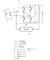
図1は、本発明の第1実施形態を示す給電装置の回路図である。なお、本発明は、非接触型、接触型の給電装置の何れにも適用可能であるが、以下の各実施形態では、本発明を非接触給電装置に適用した場合について説明する。
Hereinafter, embodiments of the present invention will be described with reference to the drawings.
FIG. 1 is a circuit diagram of a power feeding device showing a first embodiment of the present invention. Note that the present invention can be applied to both a non-contact type and a contact type power supply device, but in the following embodiments, a case where the present invention is applied to a non-contact power supply device will be described.
図1に示す非接触給電装置は、図30と同様に構成されている。すなわち、受電回路320は、ブリッジ接続された半導体スイッチQu,Qx,Qv,Qyと、各スイッチにそれぞれ逆並列に接続されたダイオードDu,Dx,Dv,Dyと、これらの素子からなるブリッジ回路の直流端子間に接続された平滑コンデンサC0と、を備えている。ブリッジ回路の交流端子間には、共振コンデンサCrと受電コイル120との直列回路が接続され、平滑コンデンサC0の両端には負荷Rが接続されている。なお、100は高周波電源、110は一次側給電線である。
一方、制御装置200は、直流端子間電圧Voと、電流検出手段CTにより検出した受電コイル120の電流iとに基づいて、スイッチQu,Qx,Qv,Qyの駆動信号を生成し、出力する。
The non-contact power feeding device shown in FIG. 1 is configured in the same manner as in FIG. That is, the
On the other hand, the
次に、図2,図3に基づいて、請求項1に対応する第1実施例の力率改善作用について説明する。
図2は、図1の受電コイル120を流れる電流i、受電コイル120の誘起電圧vin、ブリッジ回路の交流端子間電圧v及びその基本波成分v’の動作波形と、スイッチQu,Qx,Qv,Qyの駆動信号を示している。
また、図3はこのときの受電回路320の入力側等価回路であり、前記同様に、符号400は受電回路320と負荷Rとに相当するインピーダンスを示している。但し、一般的に、負荷Rに対してその他のインピーダンスは無視できるため、符号400は負荷Rに相当する純抵抗とみなすことができる。
Next, based on FIG. 2, FIG. 3, the power factor improvement effect | action of 1st Example corresponding to Claim 1 is demonstrated.
FIG. 2 shows operation waveforms of the current i flowing through the
FIG. 3 is an equivalent circuit on the input side of the
この実施例では、受電回路320の入力力率を改善するために、vの波高値が零となる期間の中点が電流iの一周期内の一方のゼロクロス点ZCPから補償期間(角度)βだけずれるように、制御装置200がスイッチQu,Qx,Qv,Qyに駆動信号を与える。この駆動信号により、vの波形は、前記中点の前後の期間(それぞれαとする)は零電圧、その他の期間は直流端子間電圧Voを波高値とする正負電圧になり、iのゼロクロス点ZCPを中心として非対称な波形となる。よって、v’の位相はiの位相とずれる。このとき、図3に示すように、v’の容量性リアクタンス成分401による電圧降下がLsにおける電圧降下vLを補償するようにβを与えると、回路のインピーダンスは見かけ上、純抵抗のみとなる。よって、iとvinとの位相が一致するため、受電回路320の入力力率を1にすることができる。
In this embodiment, in order to improve the input power factor of the
次に、入力力率を1にするための期間βの求め方を説明する。
まず、v’は、フーリエ級数展開により数式4のように表される。
![]()
First, v ′ is expressed as
![]()
一方、図3より、v’は数式7のように表すこともできる。
![]()
![]()
入力力率を1にするとき、iとvinとの位相は一致するため、iin(ωt)=Iinsin(ωt)と考えると、vin(ωt)=Vinsin(ωt)となる。従って、数式7は数式8のように表すことができる。
VL=ωLsIとおくと、数式4〜6,8より、数式9,10が成り立つ。
従って、入力力率を1にするときのβ及びαは、それぞれ数式11,12により求められる。
すなわち、電源周波数と共振周波数とが一致せずにLs≠0である場合にも、制御装置200が数式11,12によるα,βを用いて演算した駆動信号によりスイッチQu,Qx,Qv,Qyを駆動すれば、受電回路320の入力力率を1にする制御を行うことができる。
なお、配線インダクタンスが大きい場合など、他のインピーダンスの影響が大きく、図3における符号400を純抵抗と見なせない場合には、符号400に含まれるリアクタンス分も補償するように期間βを与えることで、入力力率を1とすることができる。このように符号400を純抵抗と見なせない場合の期間βの与え方については、他の第2実施例、第3実施例においても同様である。
また、vの波形が図2と同じであれば、スイッチQu,Qx,Qv,Qyの駆動信号を例えば図4のようにした場合でも、数式11,12のα,βを適用してスイッチQu,Qx,Qv,Qyを駆動すれば、受電回路320の入力力率を1にすることができる。
In other words, even when the power supply frequency and the resonance frequency do not match and L s ≠ 0, the switches Q u , Q x , and Q are controlled by the drive signal calculated by the
If the influence of other impedances is large, such as when the wiring inductance is large, and the
If the waveform of v is the same as in FIG. 2, even if the drive signals of the switches Q u , Q x , Q v , and Q y are as shown in FIG. When the switches Q u , Q x , Q v , and Q y are driven, the input power factor of the
次に、図5は本発明の第2実施形態を示す回路図であり、この非接触給電装置についても、請求項1に対応する第1実施例によって受電回路330の入力力率を1にする制御を行うことができる。
図5における受電回路330は、半導体スイッチQuにダイオードDuを逆並列接続したスイッチングアームと、半導体スイッチQxにダイオードDxを逆並列接続したスイッチングアームとを直列に接続したスイッチングアーム直列回路を備え、このスイッチングアーム直列回路と、ダイオードDv,Dyを直列接続したダイオード直列回路とを並列接続することにより、ブリッジ回路を構成している。また、ブリッジ回路の一方の直流端子(正側直流端子)にはダイオードD0のアノードが接続され、ダイオードD0のカソードとブリッジ回路の他方の直流端子(負側直流端子)との間に平滑コンデンサC0が接続されている。その他の部分は図1と同様である。
Next, FIG. 5 is a circuit diagram showing a second embodiment of the present invention. Also in this non-contact power feeding apparatus, the input power factor of the
The
図6〜図9は、図5の受電コイル120を流れる電流i、受電コイル120の誘起電圧vin、ブリッジ回路の交流端子間電圧v及びその基本波成分v’の動作波形と、スイッチQu,Qxの駆動信号とを示している。
図5の非接触給電装置において、vの波形が図2と同じであれば、スイッチQu,Qxの駆動信号を例えば図6〜図9のようにした場合でも、数式11,12のα,βを適用してスイッチQu,Qxを駆動すれば、受電回路330の入力力率を1にすることができる。
6 to 9 show the operation waveform of the current i flowing through the
5, if the waveform of v is the same as in FIG. 2, even if the drive signals of the switches Q u and Q x are as shown in FIGS. , Β are applied to drive the switches Q u , Q x , the input power factor of the
また、図10は本発明に係る給電装置の第3実施形態を示す回路図である。請求項2に記載するように、図10の給電装置を対象として第1実施例を適用した場合にも、受電回路340の入力力率を1にする制御を行うことができる。
図10における受電回路340は、半導体スイッチQxにダイオードDxを逆並列接続したスイッチングアームとダイオードDuとの直列回路と、半導体スイッチQyにダイオードDyを逆並列接続したスイッチングアームとダイオードDvとの直列回路とを並列接続することにより、ブリッジ回路が構成されている。その他の部分は図1と同様である。
FIG. 10 is a circuit diagram showing a third embodiment of the power feeding apparatus according to the present invention. As described in
Receiving circuit in FIG. 10 340, a series circuit of a switching arm and a diode D u which is connected in anti-parallel diodes D x to the semiconductor switch Q x, the switching arm and diodes connected in anti-parallel diode D y to the semiconductor switch Q y from a parallel connection of a series circuit of a D v, the bridge circuit is configured. The other parts are the same as in FIG.
図11〜図14は、図10の受電コイル120を流れる電流i、受電コイル120の誘起電圧vin、ブリッジ回路の交流端子間電圧v及びその基本波成分v’の動作波形と、スイッチQy,Qxの駆動信号とを示している。なお、図11〜図14は、図6〜図9におけるスイッチQuの駆動信号をスイッチQyに置き換えたものと同一である。
図10の非接触給電装置において、vの波形が図2と同じであれば、スイッチQy,Qxの駆動信号を例えば図11〜図14のようにした場合でも、数式11,12のα,βを適用してスイッチQy,Qxを駆動すれば、受電回路340の入力力率を1にすることができる。
11 to 14 show operation waveforms of the current i flowing through the
In the non-contact power supply apparatus of FIG. 10, if the waveform of v is the same as that of FIG. 2, even if the drive signals of the switches Q y and Q x are as shown in FIGS. , Β are applied to drive the switches Q y , Q x , the input power factor of the
次に、請求項3に対応する第2実施例の力率改善作用について説明する。
図15は、図1の受電コイル120を流れる電流i、受電コイル120の誘起電圧vin、ブリッジ回路の交流端子間電圧v及びその基本波成分v’の動作波形と、スイッチQu,Qx,Qv,Qyの駆動信号を示している。このときの受電回路320の入力側等価回路は、図3と同様である。
Next, the power factor improving action of the second embodiment corresponding to claim 3 will be described.
FIG. 15 shows operation waveforms of the current i flowing through the
この実施例においては、受電回路320の入力力率を改善するために、vの波高値が零となる期間の中点が電流iの一周期内の両方のゼロクロス点ZCPからそれぞれ補償期間(角度)βだけずれるように、制御装置200がスイッチQu,Qx,Qv,Qyに駆動信号を与える。
この駆動信号により、vの波形は、前記中点の前後の期間(それぞれα/2とする)は零電圧、その他の期間は直流端子間電圧Voを波高値とする正負電圧になり、vはiのゼロクロス点ZCPを中心として非対称な波形となる。よって、v’の位相はiの位相とずれる。このとき、図3に示すように、v’の容量性リアクタンス成分401による電圧降下がLsにおける電圧降下vLを補償するようにβを与えると、回路のインピーダンスは見かけ上、純抵抗のみとなる。よって、iとvinとの位相が一致するため、受電回路320の入力力率を1にすることができる。
In this embodiment, in order to improve the input power factor of the
With this drive signal, the waveform of v becomes a zero voltage during the period before and after the middle point (each α / 2), and becomes a positive / negative voltage with the voltage V o between the DC terminals as the peak value during the other periods. Becomes an asymmetric waveform around the zero cross point ZCP of i. Therefore, the phase of v ′ is shifted from the phase of i. At this time, as shown in FIG. 3, when β is given so that the voltage drop due to the
次に、入力力率を1にするためのβの求め方を説明する。v’は、第1実施例と同様に数式4によって表される。また、図15より、a1,b1はそれぞれ数式13,14により求められる。
第1実施例と同様にして、数式4,8,13,14より、入力力率を1にするときのβ及びαは、それぞれ数式15,16のように求められる。
従って、Ls≠0である場合にも、制御装置200が数式15,16によるα,βを用いて演算した駆動信号によりスイッチQu,Qx,Qv,Qyを駆動すれば、受電回路320の入力力率を1にする制御を行うことができる。
なお、vの波形が図15と同じであれば、スイッチQu,Qx,Qv,Qyの駆動信号を例えば図16のようにした場合でも、数式15,16のα,βを適用してスイッチQu,Qx,Qv,Qyを駆動すれば、受電回路320の入力力率を1にすることができる。
Therefore, even when L s ≠ 0, if the
If the waveform of v is the same as in FIG. 15, even if the drive signals of the switches Q u , Q x , Q v , and Q y are as shown in FIG. 16, for example, α and β in Expressions 15 and 16 are applied. When the switches Q u , Q x , Q v , and Q y are driven, the input power factor of the
更に、図17は本発明に係る給電装置の第4実施形態を示す回路図であり、第2実施例を図17の非接触給電装置に適用することも可能である。
図17に示す受電回路350は、半導体スイッチQuにダイオードDuを逆並列接続したスイッチングアームと、半導体スイッチQxにダイオードDxを逆並列接続したスイッチングアームと、を直列に接続したスイッチングアーム直列回路を備え、このスイッチングアーム直列回路と、ダイオードDv,Dyを直列接続したダイオード直列回路とを並列接続することにより、ブリッジ回路が構成されている。その他の部分は図1と同様である。なお、この受電回路350は、図5の受電回路330からダイオードD0を除去したものに相当する。
Further, FIG. 17 is a circuit diagram showing a fourth embodiment of the power feeding apparatus according to the present invention, and the second embodiment can be applied to the non-contact power feeding apparatus of FIG.
The
図18,図19は、図17の受電コイル120を流れる電流i、受電コイル120の誘起電圧vin、ブリッジ回路の交流端子間電圧v及びその基本波成分v’の動作波形と、スイッチQu,Qxの駆動信号とを示している。
図17の非接触給電装置において、vの波形が図15と同じであれば、スイッチQu,Qxの駆動信号を例えば図18,図19のようにした場合でも、数式15,16のα,βを適用してスイッチQu,Qxを駆動すれば、受電回路350の入力力率を1にすることができる。
18 and 19 show operation waveforms of the current i flowing through the
In the non-contact power supply device of FIG. 17, if the waveform of v is the same as that of FIG. 15, even if the drive signals of the switches Q u and Q x are as shown in FIGS. , Β are applied to drive the switches Q u , Q x , the input power factor of the
また、請求項4に示すように、図10の非接触給電装置に第2実施例を適用することも可能である。
図20,図21は、図10の受電コイル120を流れる電流i、受電コイル120の誘起電圧vin、ブリッジ回路の交流端子間電圧v及びその基本波成分v’の動作波形と、スイッチQy,Qxの駆動信号を示している。なお、図20,図21は、図18,図19におけるスイッチQuの駆動信号をスイッチQyに置き換えたものと同一である。
図10の非接触給電装置において、vの波形が図15と同じであれば、スイッチQy,Qxの駆動信号を例えば図20,図21のようにした場合でも、数式15,16のα,βを適用してスイッチQy,Qxを駆動すれば、受電回路340の入力力率を1にすることができる。
Further, as shown in
20 and 21 show the operation waveform of the current i flowing through the
In the non-contact power supply apparatus of FIG. 10, if the waveform of v is the same as that of FIG. 15, even if the drive signals of the switches Q y and Q x are as shown in FIGS. , Β are applied to drive the switches Q y , Q x , the input power factor of the
次いで、請求項5に対応する第3実施例の力率改善作用について説明する。
図22は、図1の受電コイル120を流れる電流i、受電コイル120の誘起電圧vin、ブリッジ回路の交流端子間電圧v及びその基本波成分v’の動作波形と、スイッチQu,Qx,Qv,Qyの駆動信号を示している。このときの受電回路320の入力側等価回路は、図3と同様である。
Next, the power factor improving action of the third embodiment corresponding to claim 5 will be described.
FIG. 22 shows operation waveforms of the current i flowing through the
この第3実施例では、受電回路320の入力力率を改善するために、電流iの一周期内でvの波高値が零となる期間αによって挟まれる期間の中点が、電流iの一周期内の二つのゼロクロス点ZCPからそれぞれ補償期間(角度)βだけずれるように、制御装置200がスイッチQu,Qx,Qv,Qyに駆動信号を与える。この駆動信号により、vの波形は、前記中点の前後の期間は直流端子間電圧Voを波高値とする正負電圧となり、その他の期間αでは零電圧となって、iのゼロクロス点ZCPを中心として非対称な波形となる。よって、v’の位相はiの位相とずれる。このとき、図3に示すように、v’の容量性リアクタンス成分401による電圧降下がLsにおける電圧降下vLを補償するようにβを与えると、回路のインピーダンスは見かけ上、純抵抗のみとなる。従って、iとvinとの位相が一致するため、受電回路320の入力力率を1にすることができる。
In the third embodiment, in order to improve the input power factor of the
次に、受電回路320の入力力率を1にするためのβの求め方を説明する。
v’は、第1実施例と同様に数式4によって表される。図22より、a1,b1はそれぞれ数式17,18のように求められる。
v ′ is expressed by
第1実施例と同様にして、数式4,8,17,18より、入力力率を1にするときのβ及びαは、それぞれ数式19,20によって求められる。
従って、Ls≠0である場合にも、制御装置200が数式19,20によるα,βを用いて演算した駆動信号によりスイッチQu,Qx,Qv,Qyを駆動すれば、受電回路320の入力力率を1にする制御を行うことができる。
なお、図1の非接触給電装置において、vの波形が図22と同じであれば、スイッチQu,Qx,Qv,Qyの駆動信号を例えば図23のようにした場合でも、数式19,20のα,βを適用してスイッチQu,Qx,Qv,Qyを駆動すれば、受電回路320の入力力率を1にすることができる。
Therefore, even when L s ≠ 0, if the
In the non-contact power feeding device of FIG. 1, if the waveform of v is the same as that of FIG. 22, even if the drive signals of the switches Q u , Q x , Q v , Q y are as shown in FIG. If the switches Q u , Q x , Q v , and Q y are driven by applying α and β of 19 and 20, the input power factor of the
同様にして、図17に示す非接触給電装置に第3実施例を適用することも可能である。
図24,図25は、図17の受電コイル120を流れる電流i、受電コイル120の誘起電圧vin、ブリッジ回路の交流端子間電圧v及びその基本波成分v’の動作波形と、スイッチQu,Qxの駆動信号を示している。
図17の非接触給電装置において、vの波形が図22と同じであれば、スイッチQu,Qxの駆動信号を例えば図24,図25のようにした場合でも、数式19,20のα,βを適用してスイッチQu,Qxを駆動すれば、受電回路350の入力力率を1にすることができる。
Similarly, the third embodiment can be applied to the non-contact power feeding apparatus shown in FIG.
FIGS. 24 and 25 show operation waveforms of the current i flowing through the
In the non-contact power supply device of FIG. 17, if the waveform of v is the same as that of FIG. 22, even if the drive signals of the switches Q u and Q x are as shown in FIGS. , Β are applied to drive the switches Q u , Q x , the input power factor of the
また、請求項6に記載するように、図10に示す非接触給電装置に第3実施例を適用することも可能である。
図26,図27は、図10の受電コイル120を流れる電流i、受電コイル120の誘起電圧vin、ブリッジ回路の交流端子間電圧v及びその基本波成分v’の動作波形と、スイッチQy,Qxの駆動信号を示している。なお、図26,図27は、図24,図25におけるスイッチQuの駆動信号をスイッチQyに置き換えたものと同一である。
図10の非接触給電装置において、vの波形が図22と同じであれば、スイッチQy,Qxの駆動信号を例えば図26,図27のようにした場合でも、数式19,20のα,βを適用してスイッチQy,Qxを駆動すれば、受電回路340の入力力率を1にすることができる。
Further, as described in claim 6, it is also possible to apply the third embodiment to the non-contact power feeding device shown in FIG.
26 and 27 show operation waveforms of the current i flowing through the
In the non-contact power supply apparatus of FIG. 10, if the waveform of v is the same as that of FIG. 22, even if the drive signals of the switches Q y and Q x are as shown in FIGS. , Β are applied to drive the switches Q y , Q x , the input power factor of the
100:高周波電源
110:一次側給電線
120:受電コイル
200:制御装置
320,330,340,350:受電回路
400:インピーダンス
401:容量性リアクタンス成分
Qu,Qx,Qv,Qy:半導体スイッチ
Du,Dx,Dv,Dy,D0:ダイオード
C0:平滑コンデンサ
Cr:共振コンデンサ
CT:電流検出手段
R:負荷
100: High-frequency power supply 110: Primary power supply line 120: Power receiving coil 200:
Claims (6)
前記受電コイルの一端が、前記受電コイルと共に共振回路を構成する共振コンデンサを介して一方の交流端子に接続され、かつ、前記受電コイルの他端が他方の交流端子に接続されたブリッジ回路と、
前記ブリッジ回路の直流端子間に接続された平滑コンデンサと、を備え、
前記平滑コンデンサの両端に負荷が接続されると共に、
前記ブリッジ回路が、半導体スイッチとダイオードとの逆並列接続回路を2個直列に接続したスイッチングアーム直列回路を少なくとも一相分、備えた給電装置において、
前記受電コイルを流れる入力電流を検出する電流検出手段と、
前記ブリッジ回路の直流端子間電圧を検出する電圧検出手段と、
前記半導体スイッチをスイッチングする制御手段と、を有し、
前記制御手段は、
前記ブリッジ回路の交流端子間電圧が、
前記入力電流の一周期内の一方のゼロクロス点から、前記共振回路に加わる電圧と前記受電コイルの誘起電圧とから算出した補償期間をずらした点を中心として、その前後に、前記補償期間と前記共振回路に加わる電圧とに基づいて算出した同一期間だけ零電圧となり、その他の期間は前記直流端子間電圧を波高値とする正負電圧になるように前記半導体スイッチをスイッチングすることを特徴とする給電装置。 A receiving coil that receives and transmits power by magnetic coupling with the outside;
A bridge circuit in which one end of the power receiving coil is connected to one AC terminal via a resonant capacitor that forms a resonance circuit together with the power receiving coil, and the other end of the power receiving coil is connected to the other AC terminal;
A smoothing capacitor connected between the DC terminals of the bridge circuit,
A load is connected to both ends of the smoothing capacitor,
In the power supply apparatus, the bridge circuit includes at least one phase of a switching arm series circuit in which two antiparallel connection circuits of a semiconductor switch and a diode are connected in series.
Current detecting means for detecting an input current flowing through the power receiving coil;
Voltage detecting means for detecting a voltage between DC terminals of the bridge circuit;
Control means for switching the semiconductor switch,
The control means includes
The voltage between the AC terminals of the bridge circuit is
Around the point where the compensation period calculated from the voltage applied to the resonance circuit and the induced voltage of the power receiving coil is shifted from one zero cross point in one cycle of the input current, before and after that, the compensation period and the The semiconductor switch is switched so as to be zero voltage only during the same period calculated based on the voltage applied to the resonance circuit, and to be positive and negative voltage with the DC terminal voltage as a peak value during the other period. apparatus.
前記受電コイルの一端が、前記受電コイルと共に共振回路を構成する共振コンデンサを介して一方の交流端子に接続され、かつ、前記受電コイルの他端が他方の交流端子に接続されたブリッジ回路と、
前記ブリッジ回路の直流端子間に接続された平滑コンデンサと、を備え、
前記平滑コンデンサの両端に負荷が接続されると共に、
前記ブリッジ回路が、半導体スイッチとダイオードとの逆並列接続回路と、ダイオードとの直列回路を、複数、並列に接続して構成される給電装置において、
前記受電コイルを流れる入力電流を検出する電流検出手段と、
前記ブリッジ回路の直流端子間電圧を検出する電圧検出手段と、
前記半導体スイッチをスイッチングする制御手段と、を有し、
前記制御手段は、
前記ブリッジ回路の交流端子間電圧が、
前記入力電流の一周期内の一方のゼロクロス点から、前記共振回路に加わる電圧と前記受電コイルの誘起電圧とから算出した補償期間をずらした点を中心として、その前後に、前記補償期間と前記共振回路に加わる電圧とに基づいて算出した同一期間だけ零電圧となり、その他の期間は前記直流端子間電圧を波高値とする正負電圧になるように前記半導体スイッチをスイッチングすることを特徴とする給電装置。 A receiving coil that receives and transmits power by magnetic coupling with the outside;
A bridge circuit in which one end of the power receiving coil is connected to one AC terminal via a resonant capacitor that forms a resonance circuit together with the power receiving coil, and the other end of the power receiving coil is connected to the other AC terminal;
A smoothing capacitor connected between the DC terminals of the bridge circuit,
A load is connected to both ends of the smoothing capacitor,
In the power supply apparatus, in which the bridge circuit is configured by connecting in parallel a plurality of parallel circuits of an antiparallel connection circuit of a semiconductor switch and a diode and a series circuit of the diode,
Current detecting means for detecting an input current flowing through the power receiving coil;
Voltage detecting means for detecting a voltage between DC terminals of the bridge circuit;
Control means for switching the semiconductor switch,
The control means includes
The voltage between the AC terminals of the bridge circuit is
Around the point where the compensation period calculated from the voltage applied to the resonance circuit and the induced voltage of the power receiving coil is shifted from one zero cross point in one cycle of the input current, before and after that, the compensation period and the The semiconductor switch is switched so as to be zero voltage only during the same period calculated based on the voltage applied to the resonance circuit, and to be positive and negative voltage with the DC terminal voltage as a peak value during the other period. apparatus.
前記受電コイルの一端が、前記受電コイルと共に共振回路を構成する共振コンデンサを介して一方の交流端子に接続され、かつ、前記受電コイルの他端が他方の交流端子に接続されたブリッジ回路と、
前記ブリッジ回路の直流端子間に接続された平滑コンデンサと、を備え、
前記平滑コンデンサの両端に負荷が接続されると共に、
前記ブリッジ回路が、半導体スイッチとダイオードとの逆並列接続回路を2個直列に接続したスイッチングアーム直列回路を少なくとも一相分、備えた給電装置において、
前記受電コイルを流れる入力電流を検出する電流検出手段と、
前記ブリッジ回路の直流端子間電圧を検出する電圧検出手段と、
前記半導体スイッチをスイッチングする制御手段と、を有し、
前記制御手段は、 前記ブリッジ回路の交流端子間電圧が、
前記入力電流の一周期内のそれぞれのゼロクロス点から、前記共振回路に加わる電圧と前記受電コイルの誘起電圧とから算出した補償期間をずらした点を中心として、その前後に、前記補償期間と前記共振回路に加わる電圧とに基づいて算出した同一期間だけ零電圧となり、その他の期間は前記直流端子間電圧を波高値とする正負電圧になるように前記半導体スイッチをスイッチングすることを特徴とする給電装置。 A receiving coil that receives and transmits power by magnetic coupling with the outside;
A bridge circuit in which one end of the power receiving coil is connected to one AC terminal via a resonant capacitor that forms a resonance circuit together with the power receiving coil, and the other end of the power receiving coil is connected to the other AC terminal;
A smoothing capacitor connected between the DC terminals of the bridge circuit,
A load is connected to both ends of the smoothing capacitor,
In the power supply apparatus, the bridge circuit includes at least one phase of a switching arm series circuit in which two antiparallel connection circuits of a semiconductor switch and a diode are connected in series.
Current detecting means for detecting an input current flowing through the power receiving coil;
Voltage detecting means for detecting a voltage between DC terminals of the bridge circuit;
Control means for switching the semiconductor switch,
The control means, the voltage between the AC terminals of the bridge circuit,
Around each point where the compensation period calculated from the voltage applied to the resonance circuit and the induced voltage of the power receiving coil is shifted from each zero cross point in one cycle of the input current, before and after the compensation period, The semiconductor switch is switched so as to be zero voltage only during the same period calculated based on the voltage applied to the resonance circuit, and to be positive and negative voltage with the DC terminal voltage as a peak value during the other period. apparatus.
前記受電コイルの一端が、前記受電コイルと共に共振回路を構成する共振コンデンサを介して一方の交流端子に接続され、かつ、前記受電コイルの他端が他方の交流端子に接続されたブリッジ回路と、
前記ブリッジ回路の直流端子間に接続された平滑コンデンサと、を備え、
前記平滑コンデンサの両端に負荷が接続されると共に、
前記ブリッジ回路が、半導体スイッチとダイオードとの逆並列接続回路と、ダイオードとの直列回路を、複数、並列に接続して構成される給電装置において、
前記受電コイルを流れる入力電流を検出する電流検出手段と、
前記ブリッジ回路の直流端子間電圧を検出する電圧検出手段と、
前記半導体スイッチをスイッチングする制御手段と、を有し、
前記制御手段は、
前記ブリッジ回路の交流端子間電圧が、
前記入力電流の一周期内のそれぞれのゼロクロス点から、前記共振回路に加わる電圧と前記受電コイルの誘起電圧とから算出した補償期間をずらした点を中心として、その前後に、前記補償期間と前記共振回路に加わる電圧とに基づいて算出した同一期間だけ零電圧となり、その他の期間は前記直流端子間電圧を波高値とする正負電圧になるように前記半導体スイッチをスイッチングすることを特徴とする給電装置。 A receiving coil that receives and transmits power by magnetic coupling with the outside;
A bridge circuit in which one end of the power receiving coil is connected to one AC terminal via a resonant capacitor that forms a resonance circuit together with the power receiving coil, and the other end of the power receiving coil is connected to the other AC terminal;
A smoothing capacitor connected between the DC terminals of the bridge circuit,
A load is connected to both ends of the smoothing capacitor,
In the power supply apparatus, in which the bridge circuit is configured by connecting in parallel a plurality of parallel circuits of an antiparallel connection circuit of a semiconductor switch and a diode and a series circuit of the diode,
Current detecting means for detecting an input current flowing through the power receiving coil;
Voltage detecting means for detecting a voltage between DC terminals of the bridge circuit;
Control means for switching the semiconductor switch,
The control means includes
The voltage between the AC terminals of the bridge circuit is
Around each point where the compensation period calculated from the voltage applied to the resonance circuit and the induced voltage of the power receiving coil is shifted from each zero cross point in one cycle of the input current, before and after the compensation period, The semiconductor switch is switched so as to be zero voltage only during the same period calculated based on the voltage applied to the resonance circuit, and to be positive and negative voltage with the DC terminal voltage as a peak value during the other period. apparatus.
前記受電コイルの一端が、前記受電コイルと共に共振回路を構成する共振コンデンサを介して一方の交流端子に接続され、かつ、前記受電コイルの他端が他方の交流端子に接続されたブリッジ回路と、
前記ブリッジ回路の直流端子間に接続された平滑コンデンサと、を備え、
前記平滑コンデンサの両端に負荷が接続されると共に、
前記ブリッジ回路が、半導体スイッチとダイオードとの逆並列接続回路を2個直列に接続したスイッチングアーム直列回路を少なくとも一相分、備えた給電装置において、
前記受電コイルを流れる入力電流を検出する電流検出手段と、
前記ブリッジ回路の直流端子間電圧を検出する電圧検出手段と、
前記半導体スイッチをスイッチングする制御手段と、を有し、
前記制御手段は、
前記ブリッジ回路の交流端子間電圧が、
前記入力電流の一周期内のそれぞれのゼロクロス点から、前記共振回路に加わる電圧と前記受電コイルの誘起電圧とから算出した補償期間をずらした点を中心として、前後に同じ期間だけ前記直流端子間電圧を波高値とする正負電圧となり、その他の期間は零電圧になるように前記半導体スイッチをスイッチングすることを特徴とする給電装置。 A receiving coil that receives and transmits power by magnetic coupling with the outside;
A bridge circuit in which one end of the power receiving coil is connected to one AC terminal via a resonant capacitor that forms a resonance circuit together with the power receiving coil, and the other end of the power receiving coil is connected to the other AC terminal;
A smoothing capacitor connected between the DC terminals of the bridge circuit,
A load is connected to both ends of the smoothing capacitor,
In the power supply apparatus, the bridge circuit includes at least one phase of a switching arm series circuit in which two antiparallel connection circuits of a semiconductor switch and a diode are connected in series.
Current detecting means for detecting an input current flowing through the power receiving coil;
Voltage detecting means for detecting a voltage between DC terminals of the bridge circuit;
Control means for switching the semiconductor switch,
The control means includes
The voltage between the AC terminals of the bridge circuit is
Between the DC terminals for the same period before and after the point where the compensation period calculated from the voltage applied to the resonance circuit and the induced voltage of the receiving coil is shifted from each zero cross point in one cycle of the input current. A power supply apparatus, wherein the semiconductor switch is switched so that the voltage becomes a positive / negative voltage having a peak value and a zero voltage in other periods.
前記受電コイルの一端が、前記受電コイルと共に共振回路を構成する共振コンデンサを介して一方の交流端子に接続され、かつ、前記受電コイルの他端が他方の交流端子に接続されたブリッジ回路と、
前記ブリッジ回路の直流端子間に接続された平滑コンデンサと、を備え、
前記平滑コンデンサの両端に負荷が接続されると共に、
前記ブリッジ回路が、半導体スイッチとダイオードとの逆並列接続回路と、ダイオードとの直列回路を、複数、並列に接続して構成される給電装置において、 前記受電コイルを流れる入力電流を検出する電流検出手段と、
前記ブリッジ回路の直流端子間電圧を検出する電圧検出手段と、
前記半導体スイッチをスイッチングする制御手段と、を有し、
前記制御手段は、
前記ブリッジ回路の交流端子間電圧が、
前記入力電流の一周期内のそれぞれのゼロクロス点から、前記共振回路に加わる電圧と前記受電コイルの誘起電圧とから算出した補償期間をずらした点を中心として、前後に同じ期間だけ前記直流端子間電圧を波高値とする正負電圧となり、その他の期間は零電圧になるように前記半導体スイッチをスイッチングすることを特徴とする給電装置。 A receiving coil that receives and transmits power by magnetic coupling with the outside;
A bridge circuit in which one end of the power receiving coil is connected to one AC terminal via a resonant capacitor that forms a resonance circuit together with the power receiving coil, and the other end of the power receiving coil is connected to the other AC terminal;
A smoothing capacitor connected between the DC terminals of the bridge circuit,
A load is connected to both ends of the smoothing capacitor,
In the power supply device in which the bridge circuit is configured by connecting a plurality of series circuits of diodes and anti-parallel connection circuits of semiconductor switches and diodes in parallel, current detection for detecting an input current flowing through the power receiving coil Means,
Voltage detecting means for detecting a voltage between DC terminals of the bridge circuit;
Control means for switching the semiconductor switch,
The control means includes
The voltage between the AC terminals of the bridge circuit is
Between the DC terminals for the same period before and after the point where the compensation period calculated from the voltage applied to the resonance circuit and the induced voltage of the receiving coil is shifted from each zero cross point in one cycle of the input current. A power supply apparatus, wherein the semiconductor switch is switched so that the voltage becomes a positive / negative voltage having a peak value and a zero voltage in other periods.
Priority Applications (3)
| Application Number | Priority Date | Filing Date | Title |
|---|---|---|---|
| JP2013123810A JP6124336B2 (en) | 2013-06-12 | 2013-06-12 | Power supply device |
| DE102014107754.7A DE102014107754A1 (en) | 2013-06-12 | 2014-06-03 | Power supply means |
| US14/300,822 US9632564B2 (en) | 2013-06-12 | 2014-06-10 | Power supply device |
Applications Claiming Priority (1)
| Application Number | Priority Date | Filing Date | Title |
|---|---|---|---|
| JP2013123810A JP6124336B2 (en) | 2013-06-12 | 2013-06-12 | Power supply device |
Publications (2)
| Publication Number | Publication Date |
|---|---|
| JP2014241698A JP2014241698A (en) | 2014-12-25 |
| JP6124336B2 true JP6124336B2 (en) | 2017-05-10 |
Family
ID=52009890
Family Applications (1)
| Application Number | Title | Priority Date | Filing Date |
|---|---|---|---|
| JP2013123810A Active JP6124336B2 (en) | 2013-06-12 | 2013-06-12 | Power supply device |
Country Status (3)
| Country | Link |
|---|---|
| US (1) | US9632564B2 (en) |
| JP (1) | JP6124336B2 (en) |
| DE (1) | DE102014107754A1 (en) |
Families Citing this family (12)
| Publication number | Priority date | Publication date | Assignee | Title |
|---|---|---|---|---|
| JP6047442B2 (en) | 2013-03-29 | 2016-12-21 | 富士電機株式会社 | Power supply device |
| JP6129669B2 (en) | 2013-07-18 | 2017-05-17 | 東海旅客鉄道株式会社 | Power supply device |
| JP6356437B2 (en) | 2014-03-03 | 2018-07-11 | 東海旅客鉄道株式会社 | Power receiving device |
| JP6361818B2 (en) * | 2015-03-31 | 2018-07-25 | Tdk株式会社 | Wireless power receiving device and wireless power transmission device |
| US9973099B2 (en) | 2015-08-26 | 2018-05-15 | Futurewei Technologies, Inc. | AC/DC converters with wider voltage regulation range |
| CN109075613B (en) * | 2016-02-02 | 2022-05-31 | 韦特里西提公司 | Controlling a wireless power transfer system |
| CN109327065B (en) * | 2018-12-06 | 2020-02-21 | 华为技术有限公司 | Receiver, method, power consumption terminal, transmitter and system of wireless charging system |
| JP7258614B2 (en) * | 2019-03-20 | 2023-04-17 | 東芝テック株式会社 | power converter |
| US20230231465A1 (en) * | 2022-01-20 | 2023-07-20 | Hengchun Mao | Advanced Power Control Techniques |
| WO2025263463A1 (en) * | 2024-06-17 | 2025-12-26 | ミラクシアエッジテクノロジー株式会社 | Non-contact power supply system |
| JP7681815B1 (en) * | 2024-09-24 | 2025-05-22 | ミラクシアエッジテクノロジー株式会社 | Non-contact power supply system |
| WO2026069724A1 (en) * | 2024-09-24 | 2026-04-02 | ミラクシアエッジテクノロジー株式会社 | Non-contact power supply system |
Family Cites Families (27)
| Publication number | Priority date | Publication date | Assignee | Title |
|---|---|---|---|---|
| US5581171A (en) | 1994-06-10 | 1996-12-03 | Northrop Grumman Corporation | Electric vehicle battery charger |
| US6160374A (en) | 1999-08-02 | 2000-12-12 | General Motors Corporation | Power-factor-corrected single-stage inductive charger |
| JP4446139B2 (en) | 2000-10-16 | 2010-04-07 | ソニー株式会社 | Image signal automatic gain control device and imaging device |
| JP4140208B2 (en) | 2001-05-22 | 2008-08-27 | 神鋼電機株式会社 | Contactless power supply |
| DE60332151D1 (en) * | 2002-12-10 | 2010-05-27 | Ebara Corp | POWER GENERATION SYSTEM FOR CONNECTION |
| DE10301978A1 (en) | 2003-01-20 | 2004-08-05 | Eurocopter Deutschland Gmbh | Device and method for transmitting and providing the energy of capacitive actuators |
| US6934167B2 (en) * | 2003-05-01 | 2005-08-23 | Delta Electronics, Inc. | Contactless electrical energy transmission system having a primary side current feedback control and soft-switched secondary side rectifier |
| TWI338996B (en) * | 2007-10-16 | 2011-03-11 | Delta Electronics Inc | Resonant converter system having synchronous rectifier control circuit and controlling method thereof |
| JP2011514137A (en) * | 2008-03-10 | 2011-04-28 | テクティウム リミテッド | Eco-friendly power supply device |
| US8923015B2 (en) | 2008-11-26 | 2014-12-30 | Auckland Uniservices Limited | Primary-side power control for inductive power transfer |
| CN102387935A (en) | 2009-04-09 | 2012-03-21 | 西门子公司 | Transmission of power bidirectionally and without contact to charge electric vehicles |
| US20110285211A1 (en) * | 2010-05-20 | 2011-11-24 | Advantest Corporation | Wireless power supply system |
| JP5348081B2 (en) * | 2010-07-07 | 2013-11-20 | 村田機械株式会社 | Non-contact power receiving device |
| NZ587357A (en) | 2010-08-13 | 2013-03-28 | Auckland Uniservices Ltd | Control circuit for pick-up in inductive power transfer system selectively shunts diodes in rectifier bridge to reduce transient disturbances to primary current |
| JP5928865B2 (en) | 2010-11-18 | 2016-06-01 | 富士電機株式会社 | Control method of non-contact power feeding device |
| JP5844631B2 (en) * | 2010-12-15 | 2016-01-20 | 東海旅客鉄道株式会社 | Power receiving device and power receiving method |
| WO2012113442A1 (en) * | 2011-02-21 | 2012-08-30 | Sma Solar Technology Ag | Dc-to-dc converter and method for operating a dc-to-dc converter |
| JP5793972B2 (en) * | 2011-06-06 | 2015-10-14 | 富士電機株式会社 | Control method of power supply device |
| US9698761B2 (en) * | 2011-08-16 | 2017-07-04 | Philips Lighting Holding B.V. | Dynamic resonant matching circuit for wireless power receivers |
| JP2013071432A (en) | 2011-09-29 | 2013-04-22 | Ricoh Co Ltd | Image forming apparatus, image forming method and image forming program |
| US8928182B2 (en) * | 2011-12-16 | 2015-01-06 | Tdk Corporation | Wireless power feeder and wireless power transmission system |
| US20150001958A1 (en) | 2012-02-09 | 2015-01-01 | Technova Inc. | Bidirectional contactless power transfer system |
| WO2014039088A1 (en) | 2012-09-07 | 2014-03-13 | Access Business Group International Llc | System and method for bidirectional wireless power transfer |
| KR20140054796A (en) | 2012-10-29 | 2014-05-09 | 삼성전기주식회사 | Power supplying apparatus and power supplying apparatus of electric vechicle |
| JP6047442B2 (en) | 2013-03-29 | 2016-12-21 | 富士電機株式会社 | Power supply device |
| TWI474573B (en) | 2013-05-14 | 2015-02-21 | Richtek Technology Corp | Wireless Power Receiver and Its Rectifier Modulation Circuit |
| JP6129669B2 (en) | 2013-07-18 | 2017-05-17 | 東海旅客鉄道株式会社 | Power supply device |
-
2013
- 2013-06-12 JP JP2013123810A patent/JP6124336B2/en active Active
-
2014
- 2014-06-03 DE DE102014107754.7A patent/DE102014107754A1/en not_active Ceased
- 2014-06-10 US US14/300,822 patent/US9632564B2/en active Active
Also Published As
| Publication number | Publication date |
|---|---|
| US9632564B2 (en) | 2017-04-25 |
| JP2014241698A (en) | 2014-12-25 |
| DE102014107754A1 (en) | 2014-12-18 |
| US20140372780A1 (en) | 2014-12-18 |
Similar Documents
| Publication | Publication Date | Title |
|---|---|---|
| JP6124336B2 (en) | Power supply device | |
| JP6129669B2 (en) | Power supply device | |
| JP6047442B2 (en) | Power supply device | |
| JP5928865B2 (en) | Control method of non-contact power feeding device | |
| JP5793972B2 (en) | Control method of power supply device | |
| JP6103445B2 (en) | Non-contact charging device power supply device | |
| CN102801328B (en) | Power supply apparatus | |
| JP6136025B2 (en) | Non-contact charging device power supply device | |
| US10044278B2 (en) | Power conversion device | |
| JPWO2015008506A1 (en) | Power feeding device and non-contact power feeding system | |
| CN105027385B (en) | Power supply device and non-contact power supply system | |
| JP2008125198A (en) | Non-contact power feeding device | |
| JP2021035077A (en) | Wireless power supply device | |
| JP6364864B2 (en) | Resonant type DC / DC converter | |
| KR102155896B1 (en) | Apparatus and Method for Wireless Battery Charging | |
| JP2017060322A (en) | Transmission equipment and non-contact power feeding system | |
| JP2022152467A (en) | Control method for DC-DC power converter | |
| Lee et al. | Design of wireless power transfer for dynamic power transmission with position-detection mechanism | |
| JP7237545B2 (en) | Electric vehicle power supply | |
| CN106026738B (en) | Inverter, power supply circuit and the method for generating alternating voltage | |
| US11929662B2 (en) | Power circuit and control method | |
| KR101843369B1 (en) | Magnetic inductive power pick-up apparatus | |
| WO2014098221A1 (en) | Converter, and bidirectional converter | |
| CN109245329B (en) | Wireless energy transmission system and method based on vector power superposition | |
| JP6854428B2 (en) | Inverter device and its control method |
Legal Events
| Date | Code | Title | Description |
|---|---|---|---|
| A621 | Written request for application examination |
Free format text: JAPANESE INTERMEDIATE CODE: A621 Effective date: 20160511 |
|
| A977 | Report on retrieval |
Free format text: JAPANESE INTERMEDIATE CODE: A971007 Effective date: 20170117 |
|
| A131 | Notification of reasons for refusal |
Free format text: JAPANESE INTERMEDIATE CODE: A131 Effective date: 20170120 |
|
| A521 | Request for written amendment filed |
Free format text: JAPANESE INTERMEDIATE CODE: A523 Effective date: 20170317 |
|
| TRDD | Decision of grant or rejection written | ||
| A01 | Written decision to grant a patent or to grant a registration (utility model) |
Free format text: JAPANESE INTERMEDIATE CODE: A01 Effective date: 20170330 |
|
| A61 | First payment of annual fees (during grant procedure) |
Free format text: JAPANESE INTERMEDIATE CODE: A61 Effective date: 20170330 |
|
| R150 | Certificate of patent or registration of utility model |
Ref document number: 6124336 Country of ref document: JP Free format text: JAPANESE INTERMEDIATE CODE: R150 |
|
| R250 | Receipt of annual fees |
Free format text: JAPANESE INTERMEDIATE CODE: R250 |
|
| R250 | Receipt of annual fees |
Free format text: JAPANESE INTERMEDIATE CODE: R250 |
|
| R250 | Receipt of annual fees |
Free format text: JAPANESE INTERMEDIATE CODE: R250 |
|
| RD02 | Notification of acceptance of power of attorney |
Free format text: JAPANESE INTERMEDIATE CODE: R3D02 |
|
| R250 | Receipt of annual fees |
Free format text: JAPANESE INTERMEDIATE CODE: R250 |
|
| R250 | Receipt of annual fees |
Free format text: JAPANESE INTERMEDIATE CODE: R250 |