JP4680453B2 - Switching power supply - Google Patents
Switching power supply Download PDFInfo
- Publication number
- JP4680453B2 JP4680453B2 JP2001289566A JP2001289566A JP4680453B2 JP 4680453 B2 JP4680453 B2 JP 4680453B2 JP 2001289566 A JP2001289566 A JP 2001289566A JP 2001289566 A JP2001289566 A JP 2001289566A JP 4680453 B2 JP4680453 B2 JP 4680453B2
- Authority
- JP
- Japan
- Prior art keywords
- power supply
- voltage
- input type
- auxiliary power
- capacitor
- Prior art date
- Legal status (The legal status is an assumption and is not a legal conclusion. Google has not performed a legal analysis and makes no representation as to the accuracy of the status listed.)
- Expired - Fee Related
Links
Images


Landscapes
- Dc-Dc Converters (AREA)
Description
【0001】
【発明の属する技術分野】
本発明はスイッチング電源に関する。
【0002】
【従来の技術】
図3は従来のコンデンサインプット型補助電源を有するスイッチング電源を示す。入力端子1、2の間には直流入力電圧が印加され、または、交流電圧がAC−DC変換部で直流電圧に変換されて入力端子1、2の間に印加される。この入力端子1、2の間に印加される直流入力電圧Vinは、コンデンサ3で平滑され、トランス4の1次巻線4aにスイッチング素子5を介して供給されるとともに、起動抵抗6を介して制御IC7に印加される。スイッチング素子5は電界効果トランジスタなどが用いられる。
【0003】
制御部としての制御IC7は、直流入力電圧Vinが起動抵抗6を介して印加されて起動し、パルス信号をスイッチング素子5に与えてオンさせる。ダイオード16及びコンデンサ17はコンデンサインプット型補助電源を構成しおり、トランス4の補助巻線4cにはその巻数に応じた電圧が発生して該電圧がダイオード16を通して制御IC7に印加されて制御IC7が安定に起動する。そして、制御IC7は周期的にパルス信号をスイッチング素子5に与えてスイッチング素子5をオン/オフさせる。
【0004】
直流入力電圧Vinはスイッチング素子5のオンオフでパルス化されてトランス4の1次巻線4aに供給される。トランス4の2次巻線4bに発生した交番電圧は、ダイオード8,9からなる整流部で整流された後にチョークコイル10及びコンデンサ11からなる平滑部で平滑されて出力端子12、13より出力されるとともに、誤差アンプ14にて設定電圧との誤差が増幅される。
【0005】
誤差アンプ14の出力信号はフォトカプラ15を介して制御IC7に入力され、制御IC7はフォトカプラ15からの入力信号により出力端子12、13の間の出力電圧が設定電圧になるようにスイッチング素子5へのパルス信号の周期を可変制御する。トランス4の補助巻線4cに発生した交番電圧は、ダイオード16で整流されてコンデンサ17により平滑されることで直流電圧Voとなり、制御IC7に供給される。
【0006】
このスイッチング電源では、トランス4の補助巻線4cには直流入力電圧Vinに応じた交番電圧が生成し、制御IC7に印加される直流電圧Voはトランス4の補助巻線4cに生成した交番電圧のピーク値に比例した電圧となる。例えば直流入力電圧Vinが150Vであるとすると、トランス4の補助巻線4cに発生する電圧は補助巻線4cの巻数により例えば直流入力電圧Vinの10%の15V程度となり、直流電圧Voも15V程度となる。従って、直流入力電圧Vinが変化すると、制御IC7に印加される直流電圧Voが大きく変動する。
【0007】
制御IC7は、補助電源から印加される直流電圧Voが例えば11V〜31Vの範囲内であるときには正常に動作するが、直流電圧Voが11V以下になると動作を停止し、直流電圧Voが31V以上になると壊れてしまう。このため、直流入力電圧Vinが変化して直流電圧Voが大きく変動すると、制御IC7は動作を停止し、又は、壊れてしまう。
【0008】
図4は、そのような不具合を改善した従来のコンデンサインプット型補助電源を有するスイッチング電源を示す。このスイッチング電源では、図3に示すスイッチング電源において、直流入力電圧Vinが変化する場合に制御IC7に印加される電圧Voを一定にするために、コンデンサインプット型補助電源には、シリーズドロッパーを構成するトランジスタ18、ツェナーダイオード19及び抵抗20とコンデンサ21を追加している。
【0009】
トランス4の補助巻線4cに発生した交番電圧は、ダイオード16で整流されてコンデンサ17で平滑されることにより直流電圧となり、トランジスタ18、ツェナーダイオード19及び抵抗20により定電圧化されてコンデンサ21に加えられ、このコンデンサ21の電圧が制御IC7に印加される。
【0010】
図5はチョークインプット型補助電源を持たせたスイッチング電源を示す。このスイッチング電源では、図4に示すスイッチング電源において、コンデンサインプット型補助電源の代りに、ダイオード22,23からなる整流部と、チョークコイル24及びコンデンサ25からなる平滑部により構成されたチョークインプット型補助電源を用いたものである。
【0011】
トランス4の補助巻線4cに発生した交番電圧は、ダイオード22,23で整流されてチョークコイル24及びコンデンサ25で平滑されることにより直流電圧Voとなり、制御IC7に印加される。この制御IC7に印加される直流電圧Voは、チョークコイル24及びコンデンサ25で平滑されたものであるから、直流入力電圧Vinが変化してもほぼ一定となる。
【0012】
【発明が解決しようとする課題】
図4に示すスイッチング電源では、直流入力電圧Vinが高いと、シリーズドロッパーの負担が増えて放熱器等が必要になり、また、効率が落ちる。
また、図6はコンデンサインプット型補助電源から制御IC7に印加される直流電圧Voの立ち上がり特性Aと、チョークインプット型補助電源から制御IC7に印加される直流電圧Voの立ち上がり特性Bを示す。なお、図6において、Tは時間を示す。図5に示すスイッチング電源では、チョークインプット型補助電源から制御IC7に印加される直流電圧Voの立ち上がりが遅いために、制御IC7は起動抵抗6で起動した後に直流電圧Voの立ち上がりの遅れにより起動不良を起こす。
本発明は、放熱器が不要で効率が良くて起動不良を起こさず、入力電圧の変動に対して安定して動作することができるスイッチング電源を提供することを目的とする。
【0013】
【課題を解決するための手段】
上記目的を達成するため、請求項1に係る発明は、直流電圧をスイッチング素子を介してトランスの1次巻線に供給して制御部からのパルス信号により前記スイッチング素子をオン/オフさせ、前記トランスの2次巻線の出力を平滑して出力するスイッチング電源において、前記直流電圧を前記制御部に印加して前記制御部を起動させる起動抵抗と、前記トランスの補助巻線の出力により前記制御部に起動時に電圧を印加するコンデンサインプット型補助電源と、前記トランスの補助巻線の出力により前記制御部に起動後に電圧を印加するチョークインプット型補助電源と、起動後に前記コンデンサインプット型補助電源を切り離すスイッチとを備えたものである。
【0014】
請求項2に係る発明は、請求項1記載のスイッチング電源において、前記コンデンサインプット型補助電源は前記補助巻線に対して前記チョークインプット型補助電源に比べて巻線数の少ない部分に接続したものである。
【0015】
【発明の実施の形態】
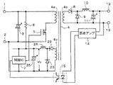
図1は本発明の一実施例を示す。この実施例は、前述した図3に示すスイッチング電源において、以下に述べるようにコンデンサインプット型補助電源とチョークインプット型補助電源とを併用した補助電源を用いるようにしたものである。なお、図1は、図3における誤差アンプ14及びフォトカプラ15の図示が省略されている。
【0016】
コンデンサインプット型補助電源は、整流部を構成するダイオード26と、シリーズドロッパーを構成するトランジスタ27、電流ダイオード28及びツェナーダイオード29と、逆流防止用ダイオード30と、コンデンサ31とからなる。
【0017】
チョークインプット型補助電源は、整流部を構成するダイオード32,33と、平滑部を構成するチョークコイル34及びコンデンサ35と、逆流防止用ダイオード36からなる。トランジスタ37、ツェナーダイオード38及び抵抗39,40は、チョークインプット型補助電源の出力電圧が所定の設定電圧以上に立ち上がったことを検出してコンデンサインプット型補助電源を停止させる制御手段(ここではスイッチ)を構成している。
【0018】
この実施例では、制御IC7は、直流入力電圧Vinが起動抵抗6を介して印加されて起動し、パルス信号をスイッチング素子5に与えてオンさせる。トランス4の補助巻線4cにはその巻数に応じた電圧が発生し、図1の点線のようにトランス4の補助巻線4cからコンデンサインプット型補助電源におけるダイオード26、トランジスタ27、ダイオード30を通してコンデンサ31に電流が流れて制御IC7に立ち上がりの早い電圧が印加されて制御IC7が安定に起動する。ここに、コンデンサインプット型補助電源は、コンデンサ31の静電容量が小さいから立ち上がりが早い。制御IC7は周期的にパルス信号をスイッチング素子5に与えてスイッチング素子5をオン/オフさせる。
【0019】
トランス4の補助巻線4cに発生した交番電圧は、コンデンサインプット型補助電源にて、ダイオード26で整流されてトランジスタ27、定電流ダイオード28及びツェナーダイオード29からなるシリーズドロッパーで定電圧化され、ダイオード30を通してコンデンサ31で平滑されて制御IC7に印加される。また、トランス4の補助巻線4cに発生した交番電圧は、チョークインプット型補助電源にて、ダイオード32,33で整流されてチョークコイル34及びコンデンサ35により平滑されて直流電圧となり、逆流防止用ダイオード36及びコンデンサ31を介して制御IC7に印加される。
【0020】
チョークインプット型補助電源の出力電圧(コンデンサ35の電圧)VAが所定の設定電圧に達すると、ツェナーダイオード38がオンしてトランジスタ37がオンし、トランジスタ27がオフしてコンデンサインプット型補助電源が停止する。よって、制御IC7の起動後には、チョークインプット型補助電源は図1の実線のように電流が流れて制御IC7に電圧を供給し、制御IC7はチョークインプット型補助電源による電圧供給で直流入力電圧Vinの変化に対して安定して動作する。
【0021】
この実施例によれば、起動時には起動抵抗6で起動されてコンデンサインプット型補助電源から立ち上がりの早い電圧が供給されるので、安定して起動し、起動不良を起こすことはない。また、コンデンサインプット型補助電源は起動時にのみ制御ICに電圧を供給すればよいので、放熱器が不要となり、効率が良い。更に、起動後にはチョークインプット型補助電源から制御ICに電圧が供給されるので、入力電圧Vinの変動に対して変動の少ない電圧を供給できる。
【0022】
ところで、コンデンサインプット型補助電源では、トランス4の補助巻線4cに発生した交番電圧のピーク値でコンデンサ31に充電するので、トランス4の補助巻線4cの巻数は通常、1〜3ターン位で充分である。また、チョークインプット型補助電源では、トランス4の補助巻線4cに発生した交番電圧を整流平滑するので、トランス4の補助巻線4cの巻数はコンデンサインプット型補助電源に比べて多くする必要がある。このため、コンデンサインプット型補助電源及びチョークインプット型補助電源を併用した上記実施例では、トランジスタ27及びダイオード26は耐圧の高いものが必要になる。
【0023】
そこで、本発明の他の実施例では、上記実施例において、トランジスタ27及びダイオード26に耐圧の高いものが要らなくなるようにしたものである。図2は本実施例の構成を示す。この実施例では、上記実施例において、トランス4の補助巻線4cの巻数は8ターンであり、チョークインプット型補助電源にはトランス4の補助巻線4cの全体(8ターン分)に発生した交番電圧をそのまま供給するが、コンデンサインプット型補助電源にはトランス4の補助巻線4cの一部(2ターン分)に発生した交番電圧を供給するようにトランス4の補助巻線4cのタップを接続している。
【0024】
従って、起動用のコンデンサインプット型補助電源は、トランス4の補助巻線4cの少ない巻線数の部分から低い電圧が供給され、トランジスタ27及びダイオード26は耐圧の高いものが要らなくなって耐圧の低いものを用いることができる。
このように、本実施例では、コンデンサインプット型補助電源は補助巻線4cに対してチョークインプット型補助電源に比べて巻線数の少ない部分に接続したので、耐圧の高い回路素子が要らなくなる。なお、図2は、図1と同様に図3における誤差アンプ14及びフォトカプラ15の図示が省略されている。
【0025】
上記実施例はフォワードコンバータ方式のスイッチング電源であったが、本発明はフライバック方式のスイッチング電源に適用して上記実施例と同様の効果を得ることができる。
【0026】
【発明の効果】
以上のように請求項1に係る発明によれば、安定して起動し、起動不良を起こすことはない。また、放熱器が不要となり、効率が良い。更に、入力電圧の変動に対して補助電源の電圧変動がほとんどなく安定して動作することができる。
請求項2に係る発明によれば、耐圧の高い回路素子が要らなくなる。
【図面の簡単な説明】
【図1】本発明の一実施例を示す回路図である。
【図2】本発明の他の実施例を示す回路図である。
【図3】従来のコンデンサインプット型補助電源を有するスイッチング電源を示す回路図である。
【図4】従来の他のコンデンサインプット型補助電源を有するスイッチング電源を示す回路図である。
【図5】チョークインプット型補助電源を持たせたスイッチング電源を示す回路図である。
【図6】コンデンサインプット型補助電源から制御ICに印加される直流電圧Voの立ち上がり特性Aと、チョークインプット型補助電源から制御ICに印加される直流電圧Voの立ち上がり特性Bを示す特性図である。
【符号の説明】
4 トランス
4c 補助巻線
5 スイッチング素子
6 起動抵抗
7 制御IC
26、30、32、、33、36 ダイオード
27 トランジスタ
28 電流ダイオード
29、38 ツェナーダイオード
31、35 コンデンサ
34 チョークコイル
39、40 抵抗[0001]
BACKGROUND OF THE INVENTION
The present invention relates to a switching power supply.
[0002]
[Prior art]
FIG. 3 shows a switching power supply having a conventional capacitor input type auxiliary power supply. A DC input voltage is applied between the
[0003]
The
[0004]
The DC input voltage Vin is pulsed by turning on and off the
[0005]
The output signal of the
[0006]
In this switching power supply, an alternating voltage corresponding to the DC input voltage Vin is generated in the
[0007]
The
[0008]
FIG. 4 shows a switching power supply having a conventional capacitor input type auxiliary power supply in which such problems are improved. In this switching power supply, the capacitor input type auxiliary power supply is configured as a series dropper in order to make the voltage Vo applied to the
[0009]
The alternating voltage generated in the
[0010]
FIG. 5 shows a switching power supply having a choke input type auxiliary power supply. In the switching power supply shown in FIG. 4, a choke input auxiliary power composed of a rectifying section composed of
[0011]
The alternating voltage generated in the
[0012]
[Problems to be solved by the invention]
In the switching power supply shown in FIG. 4, if the DC input voltage Vin is high, the burden on the series dropper increases and a radiator or the like is required, and the efficiency decreases.
FIG. 6 shows a rising characteristic A of the DC voltage Vo applied from the capacitor input type auxiliary power supply to the
It is an object of the present invention to provide a switching power supply that does not require a heatsink, has high efficiency, does not cause a start-up failure, and can operate stably against fluctuations in input voltage.
[0013]
[Means for Solving the Problems]
In order to achieve the above object, the invention according to claim 1 is directed to supplying a DC voltage to the primary winding of the transformer via the switching element to turn on / off the switching element by a pulse signal from the control unit, In a switching power supply for smoothing and outputting the output of the secondary winding of the transformer, the control is performed by applying the DC voltage to the control unit to start the control unit and the output of the auxiliary winding of the transformer A capacitor input type auxiliary power supply for applying a voltage to the control unit at the time of start-up, a choke input type auxiliary power supply for applying a voltage to the control unit after the start by the output of the auxiliary winding of the transformer, and the capacitor input type auxiliary power supply after the start-up. And a switch to be disconnected.
[0014]
The invention according to
[0015]
DETAILED DESCRIPTION OF THE INVENTION
FIG. 1 shows an embodiment of the present invention. In this embodiment, in the switching power supply shown in FIG. 3 described above, an auxiliary power supply using a capacitor input type auxiliary power supply and a choke input type auxiliary power supply is used as described below. In FIG. 1, the
[0016]
The capacitor input type auxiliary power supply includes a
[0017]
The choke input type auxiliary power source includes
[0018]
In this embodiment, the
[0019]
The alternating voltage generated in the auxiliary winding 4c of the
[0020]
When the output voltage (voltage of the capacitor 35) VA of the choke input type auxiliary power supply reaches a predetermined set voltage, the
[0021]
According to this embodiment, at the time of start-up, since the start-up
[0022]
By the way, in the capacitor input type auxiliary power supply, the
[0023]
Therefore, in another embodiment of the present invention, the
[0024]
Therefore, the capacitor input type auxiliary power supply for starting is supplied with a low voltage from the small number of windings of the auxiliary winding 4c of the
As described above, in this embodiment, the capacitor input type auxiliary power supply is connected to the auxiliary winding 4c in a portion having a smaller number of windings than the choke input type auxiliary power supply, so that a circuit element having a high withstand voltage is not required. In FIG. 2, the illustration of the
[0025]
The above embodiment is a forward converter type switching power supply, but the present invention can be applied to a flyback type switching power supply to obtain the same effect as the above embodiment.
[0026]
【The invention's effect】
As described above, according to the first aspect of the present invention, it is possible to start up stably without causing a start-up failure. In addition, a radiator is not required and efficiency is high. Further, it can operate stably with almost no voltage fluctuation of the auxiliary power supply with respect to fluctuation of the input voltage.
According to the invention of
[Brief description of the drawings]
FIG. 1 is a circuit diagram showing an embodiment of the present invention.
FIG. 2 is a circuit diagram showing another embodiment of the present invention.
FIG. 3 is a circuit diagram showing a switching power supply having a conventional capacitor input type auxiliary power supply.
FIG. 4 is a circuit diagram showing a switching power supply having another conventional capacitor input type auxiliary power supply.
FIG. 5 is a circuit diagram showing a switching power supply provided with a choke input type auxiliary power supply.
FIG. 6 is a characteristic diagram showing a rising characteristic A of the DC voltage Vo applied from the capacitor input type auxiliary power supply to the control IC and a rising characteristic B of the DC voltage Vo applied from the choke input type auxiliary power supply to the control IC. .
[Explanation of symbols]
4
26, 30, 32, 33, 36
Claims (2)
Priority Applications (1)
| Application Number | Priority Date | Filing Date | Title |
|---|---|---|---|
| JP2001289566A JP4680453B2 (en) | 2001-09-21 | 2001-09-21 | Switching power supply |
Applications Claiming Priority (1)
| Application Number | Priority Date | Filing Date | Title |
|---|---|---|---|
| JP2001289566A JP4680453B2 (en) | 2001-09-21 | 2001-09-21 | Switching power supply |
Publications (2)
| Publication Number | Publication Date |
|---|---|
| JP2003102170A JP2003102170A (en) | 2003-04-04 |
| JP4680453B2 true JP4680453B2 (en) | 2011-05-11 |
Family
ID=19112037
Family Applications (1)
| Application Number | Title | Priority Date | Filing Date |
|---|---|---|---|
| JP2001289566A Expired - Fee Related JP4680453B2 (en) | 2001-09-21 | 2001-09-21 | Switching power supply |
Country Status (1)
| Country | Link |
|---|---|
| JP (1) | JP4680453B2 (en) |
Families Citing this family (3)
| Publication number | Priority date | Publication date | Assignee | Title |
|---|---|---|---|---|
| CN101242146A (en) * | 2007-02-08 | 2008-08-13 | 王志展 | Safe, efficient and low-energy-consumption switching power supply circuit |
| JP5545839B2 (en) * | 2010-05-11 | 2014-07-09 | ニチコン株式会社 | Switching power supply |
| CN111431386A (en) * | 2020-05-29 | 2020-07-17 | 上海南芯半导体科技有限公司 | Control method and control circuit for auxiliary power supply |
Family Cites Families (3)
| Publication number | Priority date | Publication date | Assignee | Title |
|---|---|---|---|---|
| JP3141675B2 (en) * | 1994-02-28 | 2001-03-05 | 株式会社村田製作所 | Switching power supply |
| JPH1028374A (en) * | 1996-07-05 | 1998-01-27 | Nagano Japan Radio Co | Power supply |
| JPH11235027A (en) * | 1998-02-12 | 1999-08-27 | Hitachi Metals Ltd | Switching regulator |
-
2001
- 2001-09-21 JP JP2001289566A patent/JP4680453B2/en not_active Expired - Fee Related
Also Published As
| Publication number | Publication date |
|---|---|
| JP2003102170A (en) | 2003-04-04 |
Similar Documents
| Publication | Publication Date | Title |
|---|---|---|
| JP4950320B2 (en) | Switching power supply | |
| JP6424644B2 (en) | Semiconductor device for power control | |
| JP5056395B2 (en) | Switching power supply | |
| EP2621069A2 (en) | Flyback converter with primary side voltage sensing and overvoltage protection during low load operation | |
| JP6481407B2 (en) | Power supply control semiconductor device | |
| JP3236587B2 (en) | Switching power supply | |
| KR20040030446A (en) | Switching power supply | |
| CN110401347B (en) | DC power supply unit | |
| JP2004260977A (en) | AC-DC converter | |
| JP2005518177A (en) | Power converter noise reduction | |
| JP2016158399A (en) | Power supply control semiconductor device | |
| JP3425403B2 (en) | Semiconductor device and switching power supply device using this semiconductor device | |
| JP2019047655A (en) | Semiconductor device for power supply control, power supply device, discharge method of x capacitor, and switch control method | |
| US7259973B2 (en) | Semiconductor apparatus for controlling a switching power supply | |
| JP5254876B2 (en) | Power factor improved switching power supply | |
| JP7746691B2 (en) | Power circuit, power supply device | |
| JP4680453B2 (en) | Switching power supply | |
| JP5277706B2 (en) | Switching power supply | |
| JP3244424B2 (en) | Power circuit | |
| JP2013021756A (en) | Power supply device | |
| JP2004328837A (en) | Switching power supply circuit and switching regulator comprising the same | |
| JP2021072713A (en) | Switching power supply device | |
| JP2002315342A (en) | Switching power supply | |
| JP2010130881A (en) | Switching power circuit | |
| JP2008193803A (en) | Switching power supply |
Legal Events
| Date | Code | Title | Description |
|---|---|---|---|
| A621 | Written request for application examination |
Free format text: JAPANESE INTERMEDIATE CODE: A621 Effective date: 20080821 |
|
| A977 | Report on retrieval |
Free format text: JAPANESE INTERMEDIATE CODE: A971007 Effective date: 20101216 |
|
| TRDD | Decision of grant or rejection written | ||
| A01 | Written decision to grant a patent or to grant a registration (utility model) |
Free format text: JAPANESE INTERMEDIATE CODE: A01 Effective date: 20110111 |
|
| A01 | Written decision to grant a patent or to grant a registration (utility model) |
Free format text: JAPANESE INTERMEDIATE CODE: A01 |
|
| A61 | First payment of annual fees (during grant procedure) |
Free format text: JAPANESE INTERMEDIATE CODE: A61 Effective date: 20110203 |
|
| R150 | Certificate of patent or registration of utility model |
Ref document number: 4680453 Country of ref document: JP Free format text: JAPANESE INTERMEDIATE CODE: R150 Free format text: JAPANESE INTERMEDIATE CODE: R150 |
|
| FPAY | Renewal fee payment (event date is renewal date of database) |
Free format text: PAYMENT UNTIL: 20140210 Year of fee payment: 3 |
|
| S533 | Written request for registration of change of name |
Free format text: JAPANESE INTERMEDIATE CODE: R313533 |
|
| FPAY | Renewal fee payment (event date is renewal date of database) |
Free format text: PAYMENT UNTIL: 20140210 Year of fee payment: 3 |
|
| R350 | Written notification of registration of transfer |
Free format text: JAPANESE INTERMEDIATE CODE: R350 |
|
| R250 | Receipt of annual fees |
Free format text: JAPANESE INTERMEDIATE CODE: R250 |
|
| S533 | Written request for registration of change of name |
Free format text: JAPANESE INTERMEDIATE CODE: R313533 |
|
| R350 | Written notification of registration of transfer |
Free format text: JAPANESE INTERMEDIATE CODE: R350 |
|
| R250 | Receipt of annual fees |
Free format text: JAPANESE INTERMEDIATE CODE: R250 |
|
| LAPS | Cancellation because of no payment of annual fees |