JP3981612B2 - Triangular wave generator, pulse width modulation signal generator, and external synchronization / internal synchronization / asynchronous switching device - Google Patents
Triangular wave generator, pulse width modulation signal generator, and external synchronization / internal synchronization / asynchronous switching device Download PDFInfo
- Publication number
- JP3981612B2 JP3981612B2 JP2002266471A JP2002266471A JP3981612B2 JP 3981612 B2 JP3981612 B2 JP 3981612B2 JP 2002266471 A JP2002266471 A JP 2002266471A JP 2002266471 A JP2002266471 A JP 2002266471A JP 3981612 B2 JP3981612 B2 JP 3981612B2
- Authority
- JP
- Japan
- Prior art keywords
- voltage
- circuit
- triangular wave
- synchronization
- output
- Prior art date
- Legal status (The legal status is an assumption and is not a legal conclusion. Google has not performed a legal analysis and makes no representation as to the accuracy of the status listed.)
- Expired - Fee Related
Links
- 239000003990 capacitor Substances 0.000 claims description 74
- 230000010355 oscillation Effects 0.000 claims description 44
- 230000007274 generation of a signal involved in cell-cell signaling Effects 0.000 claims description 27
- 230000001360 synchronised effect Effects 0.000 claims description 24
- 238000007599 discharging Methods 0.000 claims description 8
- 230000002265 prevention Effects 0.000 claims description 5
- 230000003321 amplification Effects 0.000 claims description 3
- 238000003199 nucleic acid amplification method Methods 0.000 claims description 3
- 238000010586 diagram Methods 0.000 description 16
- 239000004575 stone Substances 0.000 description 14
- 230000000630 rising effect Effects 0.000 description 12
- 239000000872 buffer Substances 0.000 description 11
- 238000000034 method Methods 0.000 description 7
- 230000007423 decrease Effects 0.000 description 4
- 238000009499 grossing Methods 0.000 description 4
- 238000004804 winding Methods 0.000 description 4
- 230000000694 effects Effects 0.000 description 2
- 230000003247 decreasing effect Effects 0.000 description 1
- 238000005516 engineering process Methods 0.000 description 1
- 230000002452 interceptive effect Effects 0.000 description 1
- 230000007704 transition Effects 0.000 description 1
- 230000001960 triggered effect Effects 0.000 description 1
Images


Landscapes
- Dc-Dc Converters (AREA)
- Inverter Devices (AREA)
- Rectifiers (AREA)
Description
【0001】
【発明の属する技術分野】
本発明は、三角波発生装置に関する。また、本発明は、コンバータ等の電力変換器の制御等に用いられるパルス幅変調信号を生成するパルス幅変調信号生成装置に関する。また、本発明は、複数の装置を同期または非同期で運転させるための切替装置に関する。
【0002】
【従来の技術】
三角波は、三角波比較法によりパルス幅変調信号(PWM信号)を生成する場合などに用いられる(例えば、非特許文献1参照)。この三角波の発生装置として、従来より、コンデンサの充放電を繰り返すものが知られている(例えば、特許文献1、2参照)。
【0003】
図9は、従来の三角波発生装置の一例を示している。図において、三角波発生装置10は、出力端子11、コンパレータ12、スイッチSW1、SW2、電圧源14(電圧Vhiとする)、電圧源16(電圧Vloとする)、一定電流を供給する電流源S1、抵抗R1、R2、コンデンサC1、C2、入力端子18から構成されている。図中のVCCは電源線、VSSは接地線である。また、コンパレータ12の+側入力端子とコンデンサC1との接続ノードをノードAとする。なお、スイッチSW1、SW2は、コンパレータ12の出力電圧に応じて切り替わる。具体的には、ノードAの電圧がVhiに達したとき、コンパレータ12の出力電圧は低レベルから高レベルに切り替わり、スイッチSW1は電圧源14側から電圧源16側に切り替わり、スイッチSW2はオフ(開放)からオンに切り替わる。また、ノードAの電圧がVloまで下がったとき、コンパレータ12の出力電圧は高レベルから低レベルに切り替わり、スイッチSW1は電圧源16側から電圧源14側に切り替わり、スイッチSW2はオンからオフに切り替わる。
【0004】
図10は、図9の三角波発生装置の出力電圧の時間変化を示す説明図である。
以下、上述した三角波発生装置10の動作を説明する。
まず、同期信号が入力されない場合について説明する(図10(a))。時刻t0の直前まで、スイッチSW1は電圧源16側に接続されており、スイッチSW2はオンしている。このため、時刻t0の直前まで、コンデンサC1は電流源S1を通して放電している。時刻t0において、コンデンサC1の放電により、ノードAの電圧はVloまで下がる。これに同期して、コンパレータ12の出力電圧は高レベルから低レベルに切り替わり、スイッチSW1は電圧源14側に切り替わり、スイッチSW2はオフに切り替わる。このため、電源線VCCにより、抵抗R1を介してコンデンサC1は充電され始める。従って、ノードAの電圧である三角波発生装置10の出力電圧は上がる。
【0005】
ノードAの電圧がVhiに達すると(時刻t1)、コンパレータ12の出力電圧は低レベルから高レベルに切り替わり、スイッチSW1は電圧源16側に切り替わり、スイッチSW2はオンに切り替わる。このため、ノードAの電圧がVloまで下がるまで、コンデンサC1は電流源S1を通して放電する。従って、ノードAの電圧である三角波発生装置10の出力電圧は下がる。ノードAの電圧がVloまで下がると(時刻t2)、以後前記した時刻t0から時刻t2までの動作を繰り返す。
【0006】
次に、入力端子18に外部から同期信号が入力される場合について説明する(図10(b))。時刻t0の直前まで、スイッチSW1は電圧源16側に接続されており、スイッチSW2はオンしている。このため、時刻t0の直前まで、コンデンサC1は放電中であり、ノードAの電圧はVloに向けて下降中である。時刻t0において、同期信号は高レベルから低レベルに切り替わる。この立ち下がりエッジに同期して、コンデンサC1、C2を通して、ノードAの電圧は過渡的にVloまで下がる。このため、時刻t0で、スイッチSW1は電圧源14側に切り替わり、スイッチSW2はオフに切り替わる。従って、電源線VCCにより抵抗R1を介してコンデンサC1は充電され始め、三角波発生装置10の出力電圧は上がる。
【0007】
時刻t3において、同期信号の立ち上がりにより、入力端子18から、コンデンサC1、C2を通して、ノードAの電圧は過渡的にVhiまで上がる。これに同期して、スイッチSW1は電圧源16側に切り替わり、スイッチSW2はオンに切り替わる。このため、コンデンサC1は電流源S1を通して放電し、三角波発生装置10の出力電圧は下がる。この後、時刻t4において、同期信号が立ち下がると、以後前記した時刻t0から時刻t4までの動作を繰り返す。
【0008】
【特許文献1】
特開平9−172355号公報 (第4−5項、第1図)
【特許文献2】
特開平11−191725号公報 (第4−5項、第3図)
【非特許文献1】
リニアテクノロジー株式会社の、LTC1504のデータシート
インターネット<URL:http://www.linear-tech.co.jp/
datasheet/html/jp#pdf/j1504#7.pdf> (第1−5項、第3図)
【0009】
【発明が解決しようとする課題】
図9に示した三角波発生装置10では、外部からの同期信号に同期させる場合、同期信号の立ち上がり及び立ち下がりに同期して、ノードAの電圧を瞬時に変化させている。このため、三角波の上側ピーク時及び下側ピーク時に、突起状の波形が生じてしまう。
【0010】
また、充放電を繰り返すコンデンサC1の電圧を出力としているため、出力は指数関数的波形になるので、周波数やデューティ比の計算が複雑となる。
さらに、同期させる場合と、同期させない場合とで、出力される三角波の周波数が異なる。即ち、このような三角波発生装置をそれぞれ有する複数の装置を、同期させずに同時運転させた場合、各装置は互いに異なる周波数で動作する。この場合、装置間の干渉により、ノイズ及びリプルが発生してしまう。
【0011】
ところで、PWM信号により電力変換装置等を制御する場合、PWM信号の各周期内にデッドタイムが必要である。これは、例えば、一石式コンバータにおいてトランスの飽和を防止したり、フルブリッジコンバータにおいて交互にオンするはずの複数のトランジスタが同時にオンすることを防止するために必要である。このため、三角波比較法によりPWM制御信号を生成する場合、三角波発生装置とは別の回路(リミッタ等)を設けることで、PWM信号にデッドタイムを入れる必要があった。従って、パルス幅変調信号生成装置において、三角波発生装置とは別の回路を設けることなく、PWM信号にデッドタイムを入れる技術が要望されていた。
【0012】
本発明の目的は、一定の傾きで上昇及び下降する三角波の発生装置を提供することである。
本発明の別の目的は、PWM信号により制御される複数の装置を同時運転させる場合に、各装置の動作周波数を容易に同期させる技術を提供することである。
本発明の別の目的は、パルス幅変調信号生成装置において、三角波発生装置とは別の簡単な回路を設けるだけで、PWM信号にデッドタイムを入れる技術を提供することである。
【0013】
【課題を解決するための手段】
請求項1の三角波発生装置は、コンデンサと、一定電流を出力する電流源と、リセット電圧出力回路と、充放電制御回路と、充放電回路とを備え、コンデンサの電圧波形を三角波として出力する。
リセット電圧出力回路は、同期信号を受け、同期信号の立ち上がりまたは立ち下がりに同期して、同期信号の1周期より短い所定期間、第1リセット電圧を出力し、所定期間の経過後、第2リセット電圧を出力する。
【0014】
充放電制御回路は、第1リセット電圧を受けて瞬間放電電圧を出力し、第2リセット電圧を受けて放電防止電圧を出力する。
充放電回路は、放電防止電圧を受けて、電流源からの一定電流をコンデンサに供給させてコンデンサに電荷を蓄積させる。また、充放電回路は、瞬間放電電圧を受けて、コンデンサに蓄積された電荷を時間軸に対し垂直とみなせる傾きで放電させる。
【0015】
なお、リセット電圧出力回路が第1リセット電圧を出力する所定期間は、コンデンサに蓄積された電荷の放電に要する時間より長い。
また、リセット電圧出力回路は、デッドタイム信号生成回路と、スイッチと、第2リセット電圧出力回路とを備えている。
デッドタイム信号生成回路は、同期信号を受けて、同期信号の立ち上がりまたは立ち下がりに同期して、所定期間、スイッチオン電圧を出力する。また、デッドタイム信号生成回路は、所定期間の経過後、スイッチオフ電圧を出力する。
【0016】
スイッチは、スイッチオン電圧を受けてオンし、充放電制御回路を第1リセット電圧の供給源に接続する。また、スイッチは、スイッチオフ電圧を受けてオフする。
第2リセット電圧出力回路は、スイッチのオフ期間中、充放電制御回路に第2リセット電圧を入力する。
【0017】
請求項2の三角波発生装置では、同期信号は、外部回路から入力される。
請求項3の三角波発生装置は、請求項2の三角波発生装置において、内部発振回路と、選択回路とを備えていることを特徴とする。なお、内部発振回路は、外部回路から入力される同期信号の周波数と同一周波数に調整可能な同期信号を生成する。また、選択回路は、外部回路から入力される同期信号、及び内部発振回路が生成する同期信号のいずれかをリセット電圧出力回路に入力させる。
【0018】
請求項4のパルス幅変調信号生成装置は、パルス幅変調信号により制御される装置の出力電圧を検出し、内部に有する三角波発生装置を用いて、パルス幅変調信号を生成する。パルス幅変調信号生成装置は、三角波発生装置と、基準電圧を出力する基準電圧源と、誤差増幅回路と、比較器と、パルス幅変調信号出力回路とを備えている。
【0019】
三角波発生装置は、請求項1記載の三角波発生装置において、デッドタイム信号生成回路が複数の回路素子に電圧を出力可能なものである。
誤差増幅回路は、装置の出力電圧を受ける第1入力端子及び基準電圧を受ける第2入力端子を有し、装置の出力電圧と基準電圧との差を増幅した電圧を出力する。
【0020】
比較器は、三角波発生装置が出力する三角波を受ける第3入力端子、及び誤差増幅回路の出力電圧を受ける第4入力端子を有している。比較器は、三角波と誤差増幅回路の出力電圧との差に応じて、高いレベルの電圧または低いレベルの電圧を出力する。
【0021】
パルス幅変調信号出力回路は、比較器の出力電圧を受ける第5入力端子及びデッドタイム信号生成回路の出力電圧を受ける第6入力端子を有している。パルス幅変調信号出力回路は、スイッチオン電圧を受ける所定期間において、低レベルの電圧をパルス幅変調信号として出力し、スイッチオフ電圧を受ける期間において、比較器の出力電圧に応じて高レベルまたは低レベルの電圧をパルス幅変調信号として出力する。
【0022】
請求項5の外部同期/内部同期/非同期切替装置は、同期信号を生成する内部発振回路及び三角波発生装置をそれぞれ有する複数の装置を、外部同期、内部同期、非同期のいずれかで運転させる。ここで、外部同期は、複数の装置のいずれかに外部回路から入力される同期信号により、これら複数の装置を運転させるものである。内部同期は、複数の装置のいずれかの内部発振回路が生成する同期信号により、これら複数の装置を運転させるものである。非同期は、複数の装置内で内部発振回路がそれぞれ生成する同期信号により、これら複数の装置をそれぞれ運転させるものである。
【0023】
各装置が有する三角波発生装置は、請求項1記載の三角波発生装置である。
外部同期/内部同期/非同期切替装置は、複数の装置を互いに接続している共通配線と、複数の装置にそれぞれ内蔵された切替回路とを備えている。
共通配線は、外部回路から入力される同期信号、及び複数の装置のいずれかの内部発振回路が生成する同期信号を複数の装置に共通に入力させるためのものである。
【0024】
各切替回路は、各装置内で三角波発生装置、内部発振回路、及び共通配線にそれぞれ接続され、外部から入力される複数の選択信号のいずれかを受ける。各切替回路は、選択信号のレベルに応じて、外部回路から入力される同期信号を三角波発生装置に入力させる外部同期運転と、複数の装置のいずれかの内部発振回路が生成する同期信号を三角波発生装置に入力させる内部同期運転と、各装置内において各内部発振回路が生成する同期信号を各三角波発生装置に入力させる非同期運転とを切り替える。
【0025】
【発明の実施の形態】
以下、図面を用いて本発明の実施形態を説明する。
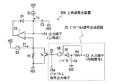
図1は、本発明に関連する三角波発生装置の実施形態を示している。図において、三角波発生装置20Aは、コンデンサC3、電流源S2、ダイオードD1、コンパレータ22、電流源S3、抵抗Rt、トランジスタTr、コンデンサC4、入力端子23、出力端子24から構成されている。図中のVCCは電源線、VSSは接地線である。三角波発生装置20Aは、外部回路(図示せず)が生成する同期信号を入力端子23に受け、コンデンサC3とコンパレータ22の−側入力端子との接続ノードの電圧を出力端子24から出力する。外部回路は、例えば、パルスジェネレータである。また、トランジスタTrのベース電流をIb、電流源S2が供給する一定電流をIs、電流源S3が供給する一定電流をIt、抵抗Rtの抵抗値をRtとする。
【0026】
以下、請求項と本実施形態との対応関係を説明する。なお、以下に示す対応関係は、参考のために一解釈を示すものであり、本発明を限定するものではない。
請求項記載のコンデンサは、コンデンサC3に対応している。
請求項記載の電流源は、電流源S2に対応している。
請求項記載のリセット電圧出力回路は、電流源S3、抵抗Rt、トランジスタTr、コンデンサC4、入力端子23に対応している。
【0027】
請求項記載のリセット電圧出力回路の出力は、抵抗Rtとコンパレータ22の+側入力端子との接続ノードの電圧に対応している。
請求項記載の第1リセット電圧は、接地線VSSの電圧に対応している。
請求項記載の第2リセット電圧は、It×Rtに相応する電圧に対応している。
【0028】
請求項記載の充放電制御回路は、コンパレータ22に対応している。
請求項記載の充放電回路は、ダイオードD1に対応している。
図2は、三角波発生装置20Aの各部の電圧の時間変化を示す説明図である。以下、図1、図2を用いて、上述した三角波発生装置20Aの動作を説明する。
時刻t0において、同期信号は高レベルに切り替わる。これに同期して、トランジスタTrに、ベース電流Ibが瞬間的に流れる。このため、トランジスタTrはオンし、コンパレータ22の+側入力端子は、接地線VSSに接続される。従って、コンパレータ22の出力は負の飽和電圧(請求項記載の瞬間放電電圧)まで下がり、ダイオードD1はオンし、コンデンサC3は放電する。即ち、三角波発生装置20Aの出力電圧は下がる。
【0029】
時刻t1において、コンデンサC3は、ほぼ完全に放電する。このとき、トランジスタTrは、オンしている。即ち、時刻t1以降、トランジスタTrがオフするまでの期間、三角波発生装置20Aの出力は0Vで一定となる。
時刻t2において、ベース電流Ibの減少によりトランジスタTrはオフする。このため、コンパレータ22の+側入力端子の電圧は、It×Rtに増加する。これにより、コンパレータ22の出力電圧は正の飽和電圧(請求項記載の放電防止電圧)まで上がり、ダイオードD1はオフする。従って、コンデンサC3は、同期信号の立ち上がりによりトランジスタTrが再びオンする(時刻t3)まで、電流源S2が供給する一定電流Isにより充電される。以後前記した時刻t0から時刻t3までの動作を繰り返す。
【0030】
なお、時刻t0から流れるベース電流Ibは、コンデンサC4の容量及びトランジスタTrのベース−エミッタ間抵抗により決まる時定数に従って、指数関数的に減少する。また、ベース電流Ibが所定値以上の期間、トランジスタTrはオンしている。従って、コンデンサC4の容量が大きいほど、ベース電流Ibは緩やかに減少し、トランジスタTrがオンしている時間は長くなる。そして、本実施形態では、ベース電流Ibが所定値以上である期間(トランジスタTrがオンしている期間、即ち、請求項記載の所定期間)が、コンデンサC3の放電時間より長くなるように、コンデンサC4の容量は設定されている。
【0031】
また、三角波のピーク電圧をVpeak、コンデンサC3の容量をCm、トランジスタTrのオフ期間の長さをtoffとすれば、ピーク電圧Vpeakは、次式で与えられる。
Vpeak=Is×toff÷Cm・・・(1)
上式を変形すれば、次式が成り立つ。
【0032】
Cm=Is×toff÷Vpeak・・・(2)
そして、コンデンサC3の容量Cmは、次式が成り立つように十分大きく設定されている。
Cm≧Is×toff÷(It×Rt)・・・(3)
ここで、(2)、(3)式により、次式が成り立つ。
【0033】
Vpeak≦It×Rt・・・(4)
このため、トランジスタTrのオフ期間において、コンデンサC3の充電電圧が、一定電流Itと抵抗Rtとの積で与えられる電圧より高くなり、コンパレータ22が負の電圧を出力してコンデンサC3が放電することはない。即ち、トランジスタTrのオフ期間において、コンデンサC3は一定電流Isにより充電され続け、出力端子24の電圧は一定の傾きで上昇し続ける。
【0034】
以上、本実施形態の三角波発生装置20Aでは、一定電流Isにより充電されるコンデンサC3の電圧を出力とした。このため、上昇期間が直線状の三角波を生成できる。
また、同期信号の立ち上がりによるトランジスタTrのオンに同期して、コンパレータ22の出力は負の飽和電圧になる。このため、コンデンサC3に蓄積された電荷は、この負の飽和電圧によりバイアスされて急峻に放電するので、放電時のコンデンサC3の電圧波形は時間軸に対してほぼ垂直になる。即ち、下降期間が直線状の三角波を生成できる。この結果、三角波の上側ピーク時及び下側ピーク時に、突起状の波形が生じることはない。
【0035】
さらに、コンデンサC3の放電時間よりトランジスタTrのオン期間が長くなるように、コンデンサC4の容量を設定した。このため、下降期間の後、上昇期間に移行するまでの期間、デッドタイムを有する三角波を生成できる。デッドタイムの長さは、コンデンサC4の容量値を適切に選ぶことで調整可能である。例えば、コンデンサC4の容量を大きくし、トランジスタTrのオン期間を同期信号の半周期間と等しくしてもよい。この場合、三角波のデッドタイムは同期信号の半周期間とほぼ等しくなり、三角波の上昇期間は短くなるので、三角波の振幅は小さくなる。
【0036】
図3は、本発明の第1の実施形態を示している。本実施形態は、請求項1に対応している。上述した図1に示した実施形態と同一部分には同一符号を付し、その説明を省略する。図3に示した三角波発生装置20Bは、コンデンサC4の代わりにデッドタイム信号生成回路25を形成したことを除いて、図1に示した実施形態の三角波生成回路20Aと同じである。
【0037】
デッドタイム信号生成回路25は、入力端子23と、抵抗Rdと、コンデンサCdと、インバータ56と、アンドゲート58と、デッドタイム信号出力端子25aとで構成されている。抵抗RdとコンデンサCdとの接続ノードをノードBとする。
《請求項との対応関係》
以下、請求項と本実施形態との対応関係を説明する。なお、以下に示す対応関係は、参考のための一解釈であり、本発明を限定するものではない。
【0038】
請求項記載のリセット電圧出力回路は、デッドタイム信号生成回路25と、トランジスタTrと、電流源S3と、抵抗Rtとに対応している。
請求項記載のスイッチオン電圧は、アンドゲート58が出力する高レベルの電圧に対応している。
【0039】
請求項記載のスイッチオフ電圧は、アンドゲート58が出力する低レベルの電圧に対応している。
請求項記載のスイッチは、トランジスタTrに対応している。
請求項記載の第1リセット電圧の供給源は、接地線VSSに対応している。
請求項記載の第2リセット電圧出力回路は、電流源S3と、抵抗Rtとに対応している。
【0040】
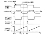
図4は、三角波発生装置20Bの各部の電圧の時間変化を示す説明図である。以下、図3、図4を用いて、上述した三角波発生装置20Bの動作を説明する。
時刻t0の直前において、コンデンサCdは放電した後であり、ノードBの電圧は接地線VSSと同じレベルである。このため、インバータ56は高レベルの電圧を出力している。また、アンドゲート58は、入力端子23から低レベルの同期信号を一方の入力端子に受けているため、低レベルの電圧を出力している。
【0041】
時刻t0において、同期信号は高レベルに切り替わる。これに同期して、インバータ56の出力電圧は高レベルに切り替わるため、アンドゲート58の出力電圧も高レベルに切り替わるので、トランジスタTrはオンする。従って、上述した図1に示した実施形態の三角波発生装置20Aと同様に、コンデンサC3は、時間軸に対してほぼ垂直とみなせる傾きで放電する。同時に、コンデンサCdは充電され始め、ノードBの電圧は、コンデンサCdの容量及び抵抗Rdの抵抗値により決まる時定数に従って、指数関数的に増加する。
【0042】
時刻t1(図示せず)において、コンデンサC3は完全に放電し、出力端子24の電圧は0Vになる。コンデンサC3に蓄積された電荷は、コンパレータ22の負の飽和電圧によりバイアスされて急峻に放電するため、時刻t1は時刻t0の直後となる。
時刻t2において、コンデンサCdの充電によりノードBの電圧はインバータ56のスレッショルド電圧(図中のVth)に達する。このため、インバータ56の出力電圧は低レベルに切り替わるため、アンドゲート58の出力電圧も低レベルに切り替わるので、トランジスタTrはオフする。従って、上述した図1に示した実施形態と同様に、コンデンサC3は充電され始め、出力端子24の電圧は上がり始める。即ち、時刻t1からt2の期間(三角波のデッドタイム)、出力端子24の電圧は0Vで一定となる。
【0043】
時刻t3において、同期信号は低レベルに切り替わる。これに同期して、コンデンサCdは放電し始める。
時刻t4において、コンデンサCdの放電によりノードBの電圧はインバータ56のスレッショルド電圧まで下がる。このため、インバータ56の出力電圧は高レベルに切り替わる。アンドゲート58は、入力端子23から低レベルの同期信号を一方の入力端子に受けているため、低レベルの電圧を引き続き出力する。従って、トランジスタTrは、時刻t2以降、時刻t4の後もオフしている。即ち、コンデンサC3は、時刻t2以降、時刻t4の後も充電され続ける。
【0044】
時刻t5において、コンデンサCdは完全に放電する。この後、同期信号が再び高レベルに切り替わると(時刻t6)、以後上述した時刻t0から時刻t5までの動作を繰り返す。
なお、本実施形態では、請求項記載の所定期間は、トランジスタTrがオンしている期間、即ち、デッドタイム信号生成回路が高レベルの電圧を出力する期間(時刻t0から時刻t2まで)に対応している。また、コンデンサC3の放電に要する時間(時刻t0から時刻t1まで)より、ノードBの電圧が接地線VSSレベルからインバータ56のスレッショルド電圧に達するまでの時間(時刻t0から時刻t2まで)の方が十分長くなるように、コンデンサCdの容量は設定されている。
【0045】
以上、本実施形態においても、上述した図1に示した実施形態と同様の効果を得ることができる。本実施形態では、時刻t1からt2の期間(三角波のデッドタイム)の長さは、コンデンサCdの容量と、抵抗Rdの抵抗値により調整できる。即ち、コンデンサCdの容量が大きいほど、ノードBの電圧は緩やかに増加するため、同期信号の立ち上がり後、インバータ56の出力電圧が低レベルに切り替わるまでの時間(時刻t0から時刻t2まで)は長くなるので、三角波のデッドタイムは長くなる。
【0046】
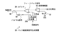
図5は、本発明の第2の実施形態を示している。本実施形態は、請求項1、請求項4に対応している。第1の実施形態と同一部分には同一符号を付し、その説明を省略する。図5に示したパルス幅変調信号生成装置26は、アンドゲート58と、インバータ56と、三角波発生装置20Bと、コンパレータ28と、誤差増幅器30と、基準電圧Vbを出力する基準電圧源32とで構成されている。
【0047】
以下、請求項と本実施形態との対応関係を説明する。なお、以下に示す対応関係は、参考のための一解釈であり、本発明を限定するものではない。
請求項記載の誤差増幅回路、第1入力端子、及び第2入力端子は、誤差増幅器30と、その−側入力端子、及び+側入力端子にそれぞれに対応している。
請求項記載の比較器、第3入力端子、及び第4入力端子は、コンパレータ28と、その+側入力端子、及び−側入力端子にそれぞれに対応している。
【0048】
請求項記載のパルス幅変調信号出力回路は、アンドゲート58及びインバータ56に対応している。
請求項記載の第5入力端子は、アンドゲート58における、コンパレータ28の出力電圧を受ける入力端子(図示せず)に対応している。
請求項記載の第6入力端子は、インバータ56の入力端子(図示せず)に対応している。
【0049】
請求項記載のパルス幅変調信号は、アンドゲート58の出力電圧に対応している。
図6は、図5のPWM信号の時間変化の一例を示す説明図である。以下、図5、図6を用いて、上述したパルス幅変調信号生成装置26の動作を説明する。
【0050】
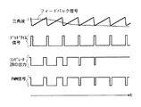
誤差増幅器30は、基準電圧Vbを+側入力端子に受け、PWM信号により制御される装置(図示せず)の出力電圧を−側入力端子に受ける。誤差増幅器30は、+側及び−側入力電圧の差を増幅し、フィードバック信号として出力する。
コンパレータ28は、+側入力端子を三角波発生装置20Bの出力端子24(図3参照)に接続され、−側入力端子を誤差増幅器30の出力に接続される。コンパレータ28は、図6に示すように、三角波の電圧がフィードバック信号より高い期間、正の飽和電圧を出力し、三角波の電圧がフィードバック信号より低い期間、負の飽和電圧を出力する。
【0051】
インバータ56は、三角波発生装置20Bのデッドタイム信号出力端子25a(図3参照)に接続される。このため、インバータ56の出力電圧(アンドゲート58の一方の入力電圧)は、三角波のデッドタイムの期間において低レベルになり、三角波におけるデッドタイムを除く期間において高レベルになる。
換言すれば、アンドゲート58は、三角波のデッドタイムの期間において、コンパレータ28の出力電圧に関係なく低レベルのPWM信号を出力する。また、アンドゲート58は、三角波におけるデッドタイムを除く期間において、コンパレータ28の出力電圧が正であれば高レベルのPWM信号を出力し、コンパレータ28の出力電圧が負であれば低レベルのPWM信号を出力する。
【0052】
上述したパルス幅変調信号生成装置26では、三角波は、前記したように、同期信号の立ち上がりエッジで、最大値から最低値(0V)まで急峻に下降する。このため、誤差増幅器30の出力電圧が正であれば、同期信号の立ち上がりエッジにより、コンパレータ28の出力電圧が正から負に必ず切り替わるので、アンドゲート58の出力電圧(PWM信号)も高レベルから低レベルに切り替わる。従って、PWM信号のトリガを容易にとることができる。
【0053】
インバータ56の出力電圧は、三角波のデッドタイムの期間において、低レベルになる。従って、アンドゲート58は、三角波のデッドタイムの期間において、コンパレータ28の出力電圧に関係なく低レベルのPWM信号を出力する。即ち、第1の実施形態の三角波発生装置20Bを用いて三角波比較法によりパルス幅変調信号生成装置を設計すれば、リミッタ等の別の回路を設けることなく、デッドタイムを有するPWM信号を容易に生成できる。
【0054】
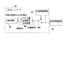
図7は、本発明の第3の実施形態を示している。本実施形態は、請求項1〜請求項3に対応している。図において、一石式コンバータ36は、内部回路38と、第2の実施形態のパルス幅変調信号生成装置26と、内部発振回路40と、スイッチSW3(請求項記載の選択回路)とで構成されている。一石式コンバータ36は、パルス幅変調信号生成装置26が生成するPWM信号により制御される。なお、一石式コンバータ36の装置外には、パルス幅変調信号生成装置26に入力するための同期信号を生成する外部発振回路42(請求項記載の外部回路)が配置されている。外部発振回路42は、例えば、パルスジェネレータである。
【0055】
内部回路38は、1次側に、トランジスタと、1次側巻線とを有している(図示せず)。また、内部回路38は、2次側に、2次側巻線と、平滑用コンデンサと、平滑用リアクトルと、ダイオードとを有している(図示せず)。一石式コンバータの詳細な回路図は公知であるので、説明を省略する。
内部発振回路40は、パルス幅変調信号生成装置26に入力するための同期信号を生成する。内部発振回路40は、この同期信号の発振周波数を変更可能であり、外部発振回路42が出力する同期信号の発振周波数を検出する(図中の点線矢印)。そして、内部発振回路40は、外部発振回路42と同じ周波数で発振する。さらに、外部発振回路42の発振周波数が変化した場合にも、内部発振回路40は、発振周波数を、外部発振回路42の発振周波数と同じに変更する。
【0056】
上述した一石式コンバータ36を単独運転させる場合、スイッチSW3は、内部発振回路40が出力する同期信号をパルス幅変調信号生成装置26における三角波発生装置20B(図5参照)に入力させる。一石式コンバータ36を他のコンバータ(図示せず)と同期運転させる場合、スイッチSW3は、外部発振回路42が出力する同期信号を三角波発生装置20Bに入力させる。
【0057】
以上、本実施形態では、内部発振回路40が出力する同期信号を、外部発振回路42が出力する同期信号と同じ周波数にした。このため、一石式コンバータ36の単独運転、或いは他のコンバータとの同期運転に拘わらず、一石式コンバータ36のパルス幅変調信号生成装置26(の三角波発生装置20B)に入力される同期信号の周波数は同じになる。従って、単独運転、或いは他のコンバータとの同期運転に拘わらず、一石式コンバータ36内の三角波の周波数及び振幅を同じにできる。従って、一石式コンバータ36と他のコンバータとが互いに異なる周波数で動作して干渉することはない。この結果、一石式コンバータ36と他のコンバータとの同時運転時にノイズ及びリプルが発生することを防止できる。
【0058】
また、パルス幅変調信号生成装置26が生成するPWM信号により一石式コンバータ36は制御される。第2の実施形態で述べたように、このPWM信号の各周期内には、デッドタイムが必ず含まれる。従って、一石式コンバータ36においてトランス(図示せず)の飽和を防止できる。
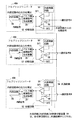
図8は、本発明の第4の実施形態を示している。本実施形態は、請求項5に対応している。図8は、本発明の外部同期/内部同期/非同期切替装置44を、複数のフルブリッジコンバータの同時運転に適用した一例を示している。図において、各フルブリッジコンバータ46A、46B〜46Nは、内部回路48と、前記したパルス幅変調信号生成装置26と、内部発振回路50と、切替回路52とで構成され、各パルス幅変調信号生成装置26が生成するPWM信号により制御される。なお、外部同期/内部同期/非同期切替装置44は、全ての切替回路52と、各切替回路52を互いに接続している共通配線54とで構成されている。
【0059】
内部回路48は、1次側に、2つずつが交互にオンする4つのトランジスタと、1次側巻線とを有している(図示せず)。また、内部回路48は、2次側に、2次側巻線と、平滑用コンデンサと、平滑用リアクトルと、ダイオードとを有している(図示せず)。フルブリッジコンバータの詳細な回路図は、従来から知られているので、説明を省略する。
【0060】
各切替回路52は、スリーステートバッファBf1、Bf2と、インバータ56とで構成されている。各切替回路52は、外部から選択信号A、B〜Nをそれぞれ受ける。また、外部回路(図示せず)が生成する同期信号は、フルブリッジコンバータ46Aの切替回路52にのみ入力される。この外部回路は、例えば、パルスジェネレータである。
【0061】
以下、各フルブリッジコンバータ46A〜46Nを外部同期、内部同期、または非同期で運転させる場合の、上述した外部同期/内部同期/非同期切替装置44の動作を、それぞれの場合に分けて説明する。
(1) 外部同期運転
各選択信号A〜Nを低レベルにする。このとき、各フルブリッジコンバータ46A〜46N内において、スリーステートバッファBf1の出力は、ハイインピーダンスになる。また、フルブリッジコンバータ46AのスリーステートバッファBf2は、外部回路からの同期信号を、フルブリッジコンバータ46Aのパルス幅変調信号生成装置26に入力すると共に、共通配線54を用いて各フルブリッジコンバータ46B〜46NのスリーステートバッファBf2にも入力する。各フルブリッジコンバータ46B〜46NのスリーステートバッファBf2は、共通配線54を介して受ける同期信号を、パルス幅変調信号生成装置26にそれぞれ入力する。従って、各フルブリッジコンバータ46A〜46Nは、外部回路からの同期信号により同期運転される。
【0062】
(2) 内部同期運転
選択信号Aを高レベルにし、他の選択信号B〜Nを低レベルにする。このとき、各フルブリッジコンバータ46B〜46NのスリーステートバッファBf1の出力は、ハイインピーダンスになる。また、フルブリッジコンバータ46AのスリーステートバッファBf1は、内部発振回路50が出力する同期信号を、フルブリッジコンバータ46Aのパルス幅変調信号生成装置26に入力すると共に、共通配線54を用いて各フルブリッジコンバータ46B〜46NのスリーステートバッファBf2にも入力する。各フルブリッジコンバータ46B〜46NのスリーステートバッファBf2は、共通配線54を介して受ける同期信号を、パルス幅変調信号生成装置26にそれぞれ入力する。即ち、各フルブリッジコンバータ46A〜46Nは、フルブリッジコンバータ46Aの内部発振回路50が生成する同期信号により同期運転される。
【0063】
(3) 非同期運転
各選択信号A〜Nを高レベルにする。このとき、各フルブリッジコンバータ46A〜46N内において、スリーステートバッファBf1は、内部発振回路50がそれぞれ出力する同期信号をパルス幅変調信号生成装置26に入力する。また、各スリーステートバッファBf2の出力は、ハイインピーダンスになる。即ち、各フルブリッジコンバータ46A〜46Nは、各フルブリッジコンバータ46A〜46N内の内部発振回路50がそれぞれ生成する同期信号により、非同期で運転される。
【0064】
以上、本実施形態の外部同期/内部同期/非同期切替装置44では、選択信号A〜Nのレベルを適切に変えるだけで、外部同期運転、内部同期運転、非同期運転を容易に切り替えることができる。従って、外部同期または内部同期で運転させることで、それぞれの装置(この例ではフルブリッジコンバータ46A〜46N)の動作周波数を容易に同期させることができる。この結果、各フルブリッジコンバータ46A〜46Nが互いに異なる周波数で動作して干渉し、ノイズまたはリプルが発生することを防止できる。
【0065】
また、各フルブリッジコンバータ46A〜46Nは、パルス幅変調信号生成装置26が生成するPWM信号によりそれぞれ制御される。第2の実施形態で述べたように、これらPWM信号の各周期内には、デッドタイムが必ず含まれる。従って、各フルブリッジコンバータ46A〜46Nにおいて、交互にオンするはずの複数のトランジスタ(図示せず)が同時にオンすることを防止できる。
【0066】
なお、上述した図1に示した実施形態では、コンデンサC3の放電に要する時間よりトランジスタTrがオンしている時間が長くなるようにコンデンサC4の容量を設定し、デッドタイムを有する三角波を生成した例を述べた。本発明はかかる実施形態に限定されるものではない。例えば、コンデンサC3の放電に要する時間とトランジスタTrがオンしている時間が同じになるようにコンデンサC4の容量を設定してもよい。この場合、デッドタイムがなく、下降期間と上昇期間とが交互に切り替わる三角波となる。
【0067】
上述した図1に示した実施形態では、同期信号の立ち上がりエッジに同期して、三角波が上昇期間から下降期間に切り替わる例を述べた。本発明はかかる実施形態に限定されるものではない。例えば、コンデンサC4と、入力端子23との間にインバータを直列に接続してもよい。この場合、同期信号の立ち下がりエッジに同期して、三角波は上昇期間から下降期間に切り替わる。
【0068】
上述した第4の実施形態では、本発明の外部同期/内部同期/非同期切替装置44を、複数の同一装置の同時運転に適用した例を述べた。本発明はかかる実施形態に限定されるものではない。本発明の外部同期/内部同期/非同期切替装置は、例えば、一石式コンバータと、フルブリッジコンバータ等の互いに異なる複数の装置の同時運転にも適用できる。
【0069】
上述した第4の実施形態では、全ての装置(フルブリッジコンバータ46A〜46N)を外部同期で運転させる例と、全ての装置を内部同期で運転させる例と、全ての装置を非同期で運転させる例とを述べた。本発明はかかる実施形態に限定されるものではない。例えば、選択信号A、Bを低レベルにし、他の全ての選択信号を高レベルにすることで、フルブリッジコンバータ46A、46Bを外部同期で運転させ、他のフルブリッジコンバータを非同期で運転させてもよい。
【0070】
【発明の効果】
本発明の三角波発生装置は、一定の傾きで上昇及び下降する三角波を生成できる。本発明の三角波発生装置は、デッドタイムを有する三角波を生成できる。このため、本発明の三角波発生装置を用いて三角波比較法によりパルス幅変調信号生成装置を設計すれば、デッドタイムを有するPWM信号を容易に生成できる。
本発明の外部同期/内部同期/非同期切替装置では、複数の装置を同時運転させる場合、それぞれの装置の動作周波数を容易に同期させることができる。
【図面の簡単な説明】
【図1】 本発明に関連する三角波発生装置を示す回路図である。
【図2】 図1の三角波発生装置の各部の電圧の時間変化を示す説明図である。
【図3】 本発明の第1の実施形態における三角波発生装置を示す回路図である。
【図4】 図3の三角波発生装置の各部の電圧の時間変化を示す説明図である。
【図5】 本発明のパルス幅変調信号生成装置を示す回路図である。
【図6】 図5のPWM信号の時間変化の一例を示す説明図である。
【図7】 本発明の第3の実施形態を示すブロック図である。
【図8】 本発明の外部同期/内部同期/非同期切替装置を、複数のフルブリッジコンバータの運転に適用した一例を示すブロック図である。
【図9】 従来の三角波発生装置の一例を示す回路図である。
【図10】 図9の三角波発生装置の出力電圧の時間変化を示す説明図である。[0001]
BACKGROUND OF THE INVENTION
The present invention relates to a triangular wave generator. The present invention also relates to a pulse width modulation signal generation device that generates a pulse width modulation signal used for controlling a power converter such as a converter. The present invention also relates to a switching device for operating a plurality of devices synchronously or asynchronously.
[0002]
[Prior art]
The triangular wave is used when a pulse width modulation signal (PWM signal) is generated by a triangular wave comparison method (for example, see Non-Patent Document 1). As this triangular wave generator, one that repeatedly charges and discharges a capacitor has been known (see, for example,
[0003]
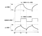
FIG. 9 shows an example of a conventional triangular wave generator. In the figure, a triangular wave generator 10 includes an output terminal 11, a
[0004]
FIG. 10 is an explanatory diagram showing the change over time of the output voltage of the triangular wave generator of FIG.
Hereinafter, the operation of the above-described triangular wave generator 10 will be described.
First, a case where a synchronization signal is not input will be described (FIG. 10A). Until immediately before time t0, the switch SW1 is connected to the
[0005]
When the voltage at the node A reaches Vhi (time t1), the output voltage of the
[0006]
Next, a case where a synchronization signal is input from the outside to the input terminal 18 will be described (FIG. 10B). Until immediately before time t0, the switch SW1 is connected to the
[0007]
At time t3, due to the rise of the synchronization signal, the voltage at the node A transiently rises to Vhi from the input terminal 18 through the capacitors C1 and C2. In synchronization with this, the switch SW1 is switched to the
[0008]
[Patent Document 1]
Japanese Patent Laid-Open No. 9-172355 (section 4-5, FIG. 1)
[Patent Document 2]
JP-A-11-191725 (Section 4-5, FIG. 3)
[Non-Patent Document 1]
LTC1504 data sheet from Linear Technology Corporation
Internet <URL: http://www.linear-tech.co.jp/
datasheet / html / jp # pdf / j1504 # 7.pdf> (Section 1-5, Figure 3)
[0009]
[Problems to be solved by the invention]
In the triangular wave generator 10 shown in FIG. 9, when synchronizing with an external synchronization signal, the voltage at the node A is instantaneously changed in synchronization with the rise and fall of the synchronization signal. For this reason, a protruding waveform is generated at the upper peak and lower peak of the triangular wave.
[0010]
In addition, since the voltage of the capacitor C1 that repeats charging and discharging is used as an output, the output is an exponential waveform, so that the calculation of the frequency and duty ratio is complicated.
Furthermore, the frequency of the output triangular wave differs depending on whether it is synchronized or not. That is, when a plurality of devices each having such a triangular wave generator are operated simultaneously without being synchronized, each device operates at a different frequency. In this case, noise and ripples are generated due to interference between apparatuses.
[0011]
By the way, when controlling a power converter etc. by a PWM signal, dead time is required in each period of a PWM signal. This is necessary, for example, to prevent transformer saturation in a one-stone converter or to prevent multiple transistors that would alternately turn on in a full-bridge converter from turning on at the same time. For this reason, when generating the PWM control signal by the triangular wave comparison method, it is necessary to provide a dead time for the PWM signal by providing a circuit (a limiter or the like) separate from the triangular wave generator. Therefore, there has been a demand for a technique for adding a dead time to a PWM signal without providing a circuit separate from the triangular wave generator in the pulse width modulation signal generator.
[0012]
An object of the present invention is to provide a triangular wave generator that rises and falls with a constant inclination.
Another object of the present invention is to provide a technique for easily synchronizing the operating frequencies of each device when a plurality of devices controlled by PWM signals are operated simultaneously.
Another object of the present invention is to provide a technique for adding a dead time to a PWM signal only by providing a simple circuit different from the triangular wave generator in the pulse width modulation signal generator.
[0013]
[Means for Solving the Problems]
The triangular wave generator of
The reset voltage output circuit receives the synchronization signal, outputs the first reset voltage for a predetermined period shorter than one cycle of the synchronization signal in synchronization with the rise or fall of the synchronization signal, and after the elapse of the predetermined period, Output voltage.
[0014]
The charge / discharge control circuit receives the first reset voltage and outputs an instantaneous discharge voltage, and receives the second reset voltage and outputs a discharge prevention voltage.
The charge / discharge circuit receives the discharge prevention voltage, supplies a constant current from the current source to the capacitor, and accumulates electric charge in the capacitor. In addition, the charge / discharge circuit receives the instantaneous discharge voltage and discharges the charge accumulated in the capacitor with a slope that can be regarded as being perpendicular to the time axis.
[0015]
In addition The predetermined period during which the reset voltage output circuit outputs the first reset voltage is longer than the time required for discharging the charge accumulated in the capacitor.
Also The reset voltage output circuit includes a dead time signal generation circuit, a switch, and a second reset voltage output circuit.
The dead time signal generation circuit receives the synchronization signal and outputs a switch-on voltage for a predetermined period in synchronization with the rising or falling edge of the synchronization signal. The dead time signal generation circuit outputs a switch-off voltage after a predetermined period.
[0016]
The switch is turned on in response to the switch-on voltage, and connects the charge / discharge control circuit to the supply source of the first reset voltage. The switch is turned off in response to the switch-off voltage.
The second reset voltage output circuit inputs the second reset voltage to the charge / discharge control circuit while the switch is off.
[0017]
Claim 2 In the triangular wave generator, the synchronization signal is input from an external circuit.
[0018]
Claim 4 The pulse width modulation signal generation device detects an output voltage of the device controlled by the pulse width modulation signal, and generates a pulse width modulation signal using a triangular wave generation device included therein. The pulse width modulation signal generation device includes a triangular wave generation device, a reference voltage source that outputs a reference voltage, an error amplification circuit, a comparator, and a pulse width modulation signal output circuit.
[0019]
The triangular wave generator is claimed in
The error amplification circuit has a first input terminal that receives the output voltage of the device and a second input terminal that receives the reference voltage, and outputs a voltage obtained by amplifying the difference between the output voltage of the device and the reference voltage.
[0020]
The comparator has a third input terminal that receives the triangular wave output from the triangular wave generator and a fourth input terminal that receives the output voltage of the error amplifier circuit. The comparator outputs a high level voltage or a low level voltage according to a difference between the triangular wave and the output voltage of the error amplifier circuit.
[0021]
The pulse width modulation signal output circuit has a fifth input terminal for receiving the output voltage of the comparator and a sixth input terminal for receiving the output voltage of the dead time signal generation circuit. The pulse width modulation signal output circuit outputs a low level voltage as a pulse width modulation signal during a predetermined period when the switch-on voltage is received, and high or low according to the output voltage of the comparator during a period when the switch-off voltage is received. The level voltage is output as a pulse width modulation signal.
[0022]
Claim 5 The external synchronization / internal synchronization / asynchronous switching device operates a plurality of devices each having an internal oscillation circuit for generating a synchronization signal and a triangular wave generating device in any of external synchronization, internal synchronization, and asynchronous. Here, the external synchronization is to operate the plurality of devices by a synchronization signal input from any external circuit to any of the plurality of devices. Internal synchronization is to operate a plurality of devices by a synchronization signal generated by any of the internal oscillation circuits of the plurality of devices. Asynchronous is to operate each of the plurality of devices by a synchronization signal generated by the internal oscillation circuit in each of the plurality of devices.
[0023]
The triangular wave generator included in each device is claimed in
The external synchronization / internal synchronization / asynchronous switching device includes a common wiring for connecting a plurality of devices to each other, and a switching circuit built in each of the plurality of devices.
The common wiring is for allowing a plurality of devices to commonly input a synchronization signal input from an external circuit and a synchronization signal generated by any of the internal oscillation circuits of the plurality of devices.
[0024]
Each switching circuit is connected to each of the triangular wave generator, the internal oscillation circuit, and the common wiring in each device, and receives one of a plurality of selection signals input from the outside. Each switching circuit has an external synchronization operation in which a synchronization signal input from an external circuit is input to the triangular wave generator according to the level of the selection signal, and a synchronization signal generated by any of the internal oscillation circuits of the plurality of devices is a triangular wave. Switching between an internal synchronous operation to be input to the generator and an asynchronous operation to input a synchronous signal generated by each internal oscillation circuit to each triangular wave generator in each device.
[0025]
DETAILED DESCRIPTION OF THE INVENTION
Hereinafter, embodiments of the present invention will be described with reference to the drawings.
FIG. 1 shows the present invention. 1 shows an embodiment of a triangular wave generator related to the above. In the figure, the triangular wave generator 20A includes a capacitor C3, a current source S2, a diode D1, a
[0026]
The correspondence between the claims and the present embodiment will be described below. In addition, the correspondence shown below shows one interpretation for reference, and does not limit this invention.
The capacitor recited in the claims corresponds to the capacitor C3.
The current source recited in the claims corresponds to the current source S2.
The reset voltage output circuit according to the claims corresponds to the current source S3, the resistor Rt, the transistor Tr, the capacitor C4, and the input terminal 23.
[0027]
The output of the reset voltage output circuit according to the claims corresponds to the voltage at the connection node between the resistor Rt and the + side input terminal of the
The first reset voltage described in the claims corresponds to the voltage of the ground line VSS.
The second reset voltage described in the claims corresponds to a voltage corresponding to It × Rt.
[0028]
The charge / discharge control circuit according to the claims corresponds to the
The charging / discharging circuit described in the claims corresponds to the diode D1.
FIG. 2 is an explanatory diagram showing the time change of the voltage of each part of the triangular wave generator 20A. Hereinafter, the operation of the above-described triangular wave generator 20A will be described with reference to FIGS.
At time t0, the synchronization signal switches to a high level. In synchronization with this, the base current Ib instantaneously flows in the transistor Tr. Therefore, the transistor Tr is turned on, and the + side input terminal of the
[0029]
At time t1, the capacitor C3 is almost completely discharged. At this time, the transistor Tr is on. That is, after the time t1, the output of the triangular wave generator 20A is constant at 0V until the transistor Tr is turned off.
At time t2, the transistor Tr is turned off due to the decrease in the base current Ib. For this reason, the voltage at the + side input terminal of the
[0030]
Note that the base current Ib flowing from time t0 decreases exponentially according to a time constant determined by the capacitance of the capacitor C4 and the base-emitter resistance of the transistor Tr. Further, the transistor Tr is on during a period when the base current Ib is equal to or greater than a predetermined value. Therefore, as the capacitance of the capacitor C4 increases, the base current Ib decreases more gradually and the time during which the transistor Tr is on becomes longer. In this embodiment, the capacitor is set such that the period during which the base current Ib is equal to or greater than the predetermined value (the period during which the transistor Tr is on, that is, the predetermined period described in the claims) is longer than the discharge time of the capacitor C3. The capacity of C4 is set.
[0031]
When the peak voltage of the triangular wave is Vpeak, the capacitance of the capacitor C3 is Cm, and the length of the off period of the transistor Tr is toff, the peak voltage Vpeak is given by the following equation.
Vpeak = Is × toff ÷ Cm (1)
If the above equation is modified, the following equation holds.
[0032]
Cm = Is * toff / Vpeak (2)
And the capacity | capacitance Cm of the capacitor | condenser C3 is set large enough so that following Formula may be formed.
Cm ≧ Is × toff ÷ (It × Rt) (3)
Here, the following equation is established by the equations (2) and (3).
[0033]
Vpeak ≦ It × Rt (4)
For this reason, during the off period of the transistor Tr, the charging voltage of the capacitor C3 becomes higher than the voltage given by the product of the constant current It and the resistance Rt, and the
[0034]
As described above, in the triangular wave generator 20A of the present embodiment, the output is the voltage of the capacitor C3 charged with the constant current Is. Therefore, it is possible to generate a triangular wave whose rising period is linear.
Further, the output of the
[0035]
Further, the capacitance of the capacitor C4 was set so that the on period of the transistor Tr was longer than the discharging time of the capacitor C3. Therefore, it is possible to generate a triangular wave having a dead time after the falling period until the transition to the rising period. The length of the dead time can be adjusted by appropriately selecting the capacitance value of the capacitor C4. For example, the capacitance of the capacitor C4 may be increased, and the on period of the transistor Tr may be made equal to the half period of the synchronization signal. In this case, the dead time of the triangular wave is substantially equal to the half period of the synchronization signal, and the rising period of the triangular wave is shortened, so that the amplitude of the triangular wave is reduced.
[0036]
FIG. 3 shows the first aspect of the present invention. 1 The embodiment of is shown. This embodiment claims 1 It corresponds to. As shown in FIG. The same parts as those in the embodiment are denoted by the same reference numerals, and the description thereof is omitted. The
[0037]
The dead time signal generation circuit 25 includes an input terminal 23, a resistor Rd, a capacitor Cd, an
<Correspondence with Claims>
The correspondence between the claims and the present embodiment will be described below. In addition, the correspondence shown below is one interpretation for reference, and does not limit the present invention.
[0038]
The reset voltage output circuit according to the claims corresponds to the dead time signal generation circuit 25, the transistor Tr, the current source S3, and the resistor Rt.
The switch-on voltage described in the claims corresponds to a high level voltage output from the AND
[0039]
The switch-off voltage described in the claims corresponds to a low level voltage output from the AND
The switch recited in the claims corresponds to the transistor Tr.
The supply source of the first reset voltage described in the claims corresponds to the ground line VSS.
The second reset voltage output circuit according to the claims corresponds to the current source S3 and the resistor Rt.
[0040]
FIG. 4 is an explanatory diagram showing the time change of the voltage of each part of the
Immediately before time t0, the capacitor Cd has been discharged, and the voltage at the node B is at the same level as the ground line VSS. Therefore, the
[0041]
At time t0, the synchronization signal switches to a high level. In synchronization with this, since the output voltage of the
[0042]
At time t1 (not shown), the capacitor C3 is completely discharged, and the voltage at the output terminal 24 becomes 0V. Since the electric charge accumulated in the capacitor C3 is biased by the negative saturation voltage of the
At time t2, the voltage of the node B reaches the threshold voltage of the inverter 56 (Vth in the figure) by charging the capacitor Cd. For this reason, since the output voltage of the
[0043]
At time t3, the synchronization signal switches to a low level. In synchronization with this, the capacitor Cd starts to discharge.
At time t4, the voltage at node B drops to the threshold voltage of
[0044]
At time t5, the capacitor Cd is completely discharged. Thereafter, when the synchronization signal switches to the high level again (time t6), the operation from time t0 to time t5 described above is repeated thereafter.
In the present embodiment, the predetermined period described in the claims corresponds to a period in which the transistor Tr is on, that is, a period in which the dead time signal generation circuit outputs a high level voltage (from time t0 to time t2). is doing. Further, the time (from time t0 to time t2) until the voltage of the node B reaches the threshold voltage of the
[0045]
As described above, this embodiment also described above. As shown in FIG. The same effect as the embodiment can be obtained. In the present embodiment, the length of the period (triangular wave dead time) from time t1 to t2 can be adjusted by the capacitance of the capacitor Cd and the resistance value of the resistor Rd. That is, as the capacitance of the capacitor Cd increases, the voltage at the node B increases more gradually. Therefore, the time (from time t0 to time t2) until the output voltage of the
[0046]
FIG. 5 shows the first aspect of the present invention. 2 The embodiment of is shown. This embodiment claims 1. Claim 4 It corresponds to. First 1's The same parts as those in the embodiment are denoted by the same reference numerals, and the description thereof is omitted. The pulse width
[0047]
The correspondence between the claims and the present embodiment will be described below. In addition, the correspondence shown below is one interpretation for reference, and does not limit the present invention.
The error amplifying circuit, the first input terminal, and the second input terminal described in the claims correspond to the error amplifier 30 and its − side input terminal and + side input terminal, respectively.
The comparator, the third input terminal, and the fourth input terminal described in the claims correspond to the comparator 28 and its + side input terminal and − side input terminal, respectively.
[0048]
The pulse width modulation signal output circuit according to the claims corresponds to the AND
The fifth input terminal described in the claims corresponds to an input terminal (not shown) that receives the output voltage of the comparator 28 in the AND
The sixth input terminal described in the claims corresponds to an input terminal (not shown) of the
[0049]
The pulse width modulation signal described in the claims corresponds to the output voltage of the AND
FIG. 6 is an explanatory diagram showing an example of a time change of the PWM signal of FIG. Hereinafter, the operation of the above-described pulse width modulation
[0050]
The error amplifier 30 receives the reference voltage Vb at the + side input terminal, and receives the output voltage of a device (not shown) controlled by the PWM signal at the − side input terminal. The error amplifier 30 amplifies the difference between the + side input voltage and the − side input voltage and outputs it as a feedback signal.
The comparator 28 has a + side input terminal connected to the output terminal 24 (see FIG. 3) of the
[0051]
The
In other words, the AND
[0052]
In the pulse width modulation
[0053]
The output voltage of the
[0054]
FIG. 7 shows the first aspect of the present invention. 3 The embodiment of is shown. This embodiment is claimed in
[0055]
The
The
[0056]
When the above-described single-
[0057]
As described above, in the present embodiment, the synchronization signal output from the
[0058]
Further, the one-
FIG. 8 shows the first aspect of the present invention. 4 The embodiment of is shown. This embodiment claims 5 It corresponds to. FIG. 8 shows an example in which the external synchronous / internal synchronous / asynchronous switching device 44 of the present invention is applied to the simultaneous operation of a plurality of full bridge converters. In the figure, each full-
[0059]
The
[0060]
Each switching circuit 52 includes three-state buffers Bf1 and Bf2 and an
[0061]
Hereinafter, the operation of the external synchronization / internal synchronization / asynchronous switching device 44 described above when each of the full bridge converters 46A to 46N is operated in an external synchronization, internal synchronization, or asynchronous manner will be described separately for each case.
(1) External synchronous operation
Each selection signal A to N is set to a low level. At this time, in each of the full bridge converters 46A to 46N, the output of the three-state buffer Bf1 becomes high impedance. Further, the three-state buffer Bf2 of the full bridge converter 46A inputs the synchronization signal from the external circuit to the pulse width modulation
[0062]
(2) Internal synchronous operation
The selection signal A is set to the high level, and the other selection signals B to N are set to the low level. At this time, the outputs of the three-state buffers Bf1 of the full-
[0063]
(3) Asynchronous operation
Each selection signal A to N is set to a high level. At this time, in each of the full bridge converters 46 </ b> A to 46 </ b> N, the three-state buffer Bf <b> 1 inputs the synchronization signal output from the
[0064]
As described above, in the external synchronization / internal synchronization / asynchronous switching device 44 of this embodiment, it is possible to easily switch between the external synchronous operation, the internal synchronous operation, and the asynchronous operation only by appropriately changing the levels of the selection signals A to N. Therefore, by operating with external synchronization or internal synchronization, the operating frequencies of the respective devices (full bridge converters 46A to 46N in this example) can be easily synchronized. As a result, it is possible to prevent the full bridge converters 46A to 46N from operating at different frequencies and interfering with each other to generate noise or ripple.
[0065]
Each of the full bridge converters 46 </ b> A to 46 </ b> N is controlled by a PWM signal generated by the pulse width modulation
[0066]
As mentioned above As shown in FIG. In the embodiment, an example has been described in which the capacitance of the capacitor C4 is set so that the time during which the transistor Tr is on is longer than the time required for discharging the capacitor C3, and a triangular wave having a dead time is generated. The present invention is not limited to such an embodiment. For example, the capacitance of the capacitor C4 may be set so that the time required for discharging the capacitor C3 and the time during which the transistor Tr is on are the same. In this case, there is no dead time, and a triangular wave in which the falling period and the rising period are alternately switched is obtained.
[0067]
Mentioned above As shown in FIG. In the embodiment, the example in which the triangular wave is switched from the rising period to the falling period in synchronization with the rising edge of the synchronization signal has been described. The present invention is not limited to such an embodiment. For example, an inverter may be connected in series between the capacitor C4 and the input terminal 23. In this case, the triangular wave is switched from the rising period to the falling period in synchronization with the falling edge of the synchronization signal.
[0068]
No. mentioned above 4 In the above embodiment, the example in which the external synchronization / internal synchronization / asynchronous switching device 44 of the present invention is applied to the simultaneous operation of a plurality of the same devices has been described. The present invention is not limited to such an embodiment. The external synchronous / internal synchronous / asynchronous switching device of the present invention can also be applied to simultaneous operation of a plurality of different devices such as a one-stone converter and a full bridge converter.
[0069]
No. mentioned above 4 In the embodiment, an example in which all devices (full-bridge converters 46A to 46N) are operated in external synchronization, an example in which all devices are operated in internal synchronization, and an example in which all devices are operated asynchronously has been described. . The present invention is not limited to such an embodiment. For example, by setting the selection signals A and B to a low level and all other selection signals to a high level, the
[0070]
【The invention's effect】
The triangular wave generator of the present invention can generate a triangular wave that rises and falls with a constant slope. The triangular wave generator of the present invention can generate a triangular wave having a dead time. For this reason, if a pulse width modulation signal generator is designed by the triangular wave comparison method using the triangular wave generator of the present invention, a PWM signal having a dead time can be easily generated.
In the external synchronization / internal synchronization / asynchronous switching device of the present invention, when a plurality of devices are operated simultaneously, the operating frequencies of the respective devices can be easily synchronized.
[Brief description of the drawings]
FIG. 1 shows the present invention. is connected with It is a circuit diagram which shows a triangular wave generator.
FIG. 2 is an explanatory diagram showing a change in voltage of each part of the triangular wave generator of FIG. 1 with time.
FIG. 3 shows the first aspect of the present invention. 1 It is a circuit diagram which shows the triangular wave generator in the embodiment.
4 is an explanatory diagram showing a change in voltage of each part of the triangular wave generator of FIG. 3 with time.
FIG. 5 is a circuit diagram showing a pulse width modulation signal generating apparatus of the present invention.
6 is an explanatory diagram showing an example of a time change of the PWM signal in FIG. 5;
FIG. 7 shows the first of the present invention. 3 It is a block diagram which shows this embodiment.
FIG. 8 is a block diagram showing an example in which the external synchronous / internal synchronous / asynchronous switching device of the present invention is applied to the operation of a plurality of full bridge converters.
FIG. 9 is a circuit diagram showing an example of a conventional triangular wave generator.
10 is an explanatory diagram showing a change over time of the output voltage of the triangular wave generator of FIG. 9;
Claims (5)
一定電流を出力する電流源と、
同期信号を受け、前記同期信号の立ち上がりまたは立ち下がりに同期して、前記同期信号の1周期より短い所定期間、第1リセット電圧を出力し、前記所定期間の経過後、第2リセット電圧を出力するリセット電圧出力回路と、
前記第1リセット電圧を受けて瞬間放電電圧を出力し、前記第2リセット電圧を受けて放電防止電圧を出力する充放電制御回路と、
前記放電防止電圧を受けて、前記一定電流を前記コンデンサに供給させて前記コンデンサに電荷を蓄積させ、かつ前記瞬間放電電圧を受けて、前記コンデンサに蓄積された電荷を時間軸に対し垂直とみなせる傾きで放電させる充放電回路とを備え、
前記リセット電圧出力回路が前記第1リセット電圧を出力する前記所定期間は、前記蓄積された電荷の放電に要する時間より長く、
前記リセット電圧出力回路は、
前記同期信号を受けて、前記同期信号の立ち上がりまたは立ち下がりに同期して、前記所定期間、スイッチオン電圧を出力し、前記所定期間の経過後、スイッチオフ電圧を出力するデッドタイム信号生成回路と、
前記スイッチオン電圧を受けてオンし、前記充放電制御回路を第1リセット電圧の供給源に接続し、前記スイッチオフ電圧を受けてオフするスイッチと、
前記スイッチのオフ期間中、前記充放電制御回路に前記第2リセット電圧を入力する第2リセット電圧出力回路と
を備えていることを特徴とする三角波発生装置。In the triangular wave generator that outputs the voltage waveform of the capacitor as a triangular wave,
A current source that outputs a constant current;
In response to the synchronization signal, the first reset voltage is output for a predetermined period shorter than one cycle of the synchronization signal in synchronization with the rise or fall of the synchronization signal, and the second reset voltage is output after the predetermined period has elapsed. Reset voltage output circuit to
A charge / discharge control circuit that receives the first reset voltage to output an instantaneous discharge voltage and receives the second reset voltage to output a discharge prevention voltage;
In response to the discharge prevention voltage, the constant current is supplied to the capacitor to accumulate electric charge in the capacitor, and the electric charge accumulated in the capacitor is considered to be perpendicular to the time axis by receiving the instantaneous discharge voltage. A charge / discharge circuit that discharges at an inclination ,
The predetermined period during which the reset voltage output circuit outputs the first reset voltage is longer than the time required for discharging the accumulated charge,
The reset voltage output circuit includes:
A dead time signal generation circuit that receives the synchronization signal, outputs a switch-on voltage for the predetermined period in synchronization with a rise or fall of the synchronization signal, and outputs a switch-off voltage after the predetermined period has elapsed; ,
A switch that turns on in response to the switch-on voltage, connects the charge / discharge control circuit to a supply source of a first reset voltage, and that turns off in response to the switch-off voltage;
A triangular wave generator comprising: a second reset voltage output circuit that inputs the second reset voltage to the charge / discharge control circuit during an off period of the switch .
前記同期信号は、外部回路から入力されることを特徴とする三角波発生装置。In the triangular wave generator according to claim 1,
The synchronization signal is input from an external circuit .
前記外部回路から入力される同期信号の周波数と同一周波数に調整可能な同期信号を生成する内部発振回路と、
前記外部回路から入力される同期信号、及び前記内部発振回路が生成する同期信号のいずれかを前記リセット電圧出力回路に入力させる選択回路と
を備えていることを特徴とする三角波発生装置。In the triangular wave generator according to claim 2,
An internal oscillation circuit that generates a synchronization signal adjustable to the same frequency as the frequency of the synchronization signal input from the external circuit;
A triangular wave generator comprising: a selection circuit that inputs either a synchronization signal input from the external circuit or a synchronization signal generated by the internal oscillation circuit to the reset voltage output circuit .
前記三角波発生装置は、請求項1記載の三角波発生装置において、前記デッドタイム信号生成回路が複数の回路素子に電圧を出力可能なものであり、The triangular wave generating device according to claim 1, wherein the dead time signal generating circuit is capable of outputting a voltage to a plurality of circuit elements.
基準電圧を出力する基準電圧源と、A reference voltage source for outputting a reference voltage;
前記装置の出力電圧を受ける第1入力端子及び前記基準電圧を受ける第2入力端子を有し、前記装置の出力電圧と前記基準電圧との差を増幅した電圧を出力する誤差増幅回路と、An error amplification circuit having a first input terminal for receiving the output voltage of the device and a second input terminal for receiving the reference voltage, and outputting a voltage obtained by amplifying the difference between the output voltage of the device and the reference voltage;
前記三角波発生装置が出力する前記三角波を受ける第3入力端子及び前記誤差増幅回路の出力電圧を受ける第4入力端子を有し、前記三角波と前記誤差増幅回路の出力電圧との差に応じて、高いレベルの電圧または低いレベルの電圧を出力する比較器と、A third input terminal for receiving the triangular wave output from the triangular wave generator and a fourth input terminal for receiving the output voltage of the error amplifier circuit, and depending on the difference between the triangular wave and the output voltage of the error amplifier circuit; A comparator that outputs a high level voltage or a low level voltage;
前記比較器の出力電圧を受ける第5入力端子及び前記デッドタイム信号生成回路の出力電圧を受ける第6入力端子を有し、前記スイッチオン電圧を受ける前記所定期間において、低レベルの電圧を前記パルス幅変調信号として出力し、前記スイッチオフ電圧を受ける期間において、前記比較器の出力電圧のレベルに応じて高レベルまたは前記低レベルの電圧を前記パルス幅変調信号として出力するパルス幅変調信号出力回路とA fifth input terminal for receiving the output voltage of the comparator and a sixth input terminal for receiving the output voltage of the dead time signal generation circuit; A pulse width modulation signal output circuit for outputting a high level or a low level voltage as the pulse width modulation signal according to the level of the output voltage of the comparator during a period of outputting as a width modulation signal and receiving the switch-off voltage When
を備えていることを特徴とするパルス幅変調信号生成装置。A pulse width modulation signal generating device comprising:
前記三角波発生装置は、請求項1記載の三角波発生装置であり、 The triangular wave generator is the triangular wave generator according to claim 1,
前記外部回路から入力される同期信号、及び前記複数の装置のいずれかの前記内部発振回路が生成する同期信号を前記複数の装置に共通に入力させるために、前記複数の装置を互いに接続している共通配線と、The plurality of devices are connected to each other in order to commonly input the synchronization signal input from the external circuit and the synchronization signal generated by the internal oscillation circuit of any of the plurality of devices to the plurality of devices. Common wiring and
前記複数の装置にそれぞれ内蔵され、前記各装置内で前記三角波発生装置、前記内部発振回路、及び前記共通配線にそれぞれ接続され、外部から入力される複数の選択信号のいずれかを受けて、前記選択信号のレベルに応じて、前記外部回路から入力される同期信号を前記三角波発生装置に入力させる外部同期運転と、前記複数の装置のいずれかの前記内部発振回路が生成する同期信号を前記三角波発生装置に入力させる内部同期運転と、前記各装置内において前記各内部発振回路が生成する同期信号を前記各三角波発生装置に入力させる非同期運転とを切り替える切替回路とBuilt in each of the plurality of devices, each connected to the triangular wave generator, the internal oscillation circuit, and the common wiring in each device, receiving any one of a plurality of selection signals input from the outside, In accordance with the level of the selection signal, an external synchronous operation for inputting a synchronous signal input from the external circuit to the triangular wave generator, and a synchronous signal generated by the internal oscillation circuit of any of the plurality of devices is the triangular wave. A switching circuit for switching between an internal synchronous operation to be input to the generator and an asynchronous operation to input a synchronous signal generated by each internal oscillation circuit to each triangular wave generator in each device
を備えていることを特徴とする外部同期/内部同期/非同期切替装置。An external synchronization / internal synchronization / asynchronous switching device characterized by comprising:
Priority Applications (1)
| Application Number | Priority Date | Filing Date | Title |
|---|---|---|---|
| JP2002266471A JP3981612B2 (en) | 2002-09-12 | 2002-09-12 | Triangular wave generator, pulse width modulation signal generator, and external synchronization / internal synchronization / asynchronous switching device |
Applications Claiming Priority (1)
| Application Number | Priority Date | Filing Date | Title |
|---|---|---|---|
| JP2002266471A JP3981612B2 (en) | 2002-09-12 | 2002-09-12 | Triangular wave generator, pulse width modulation signal generator, and external synchronization / internal synchronization / asynchronous switching device |
Publications (2)
| Publication Number | Publication Date |
|---|---|
| JP2004104645A JP2004104645A (en) | 2004-04-02 |
| JP3981612B2 true JP3981612B2 (en) | 2007-09-26 |
Family
ID=32265282
Family Applications (1)
| Application Number | Title | Priority Date | Filing Date |
|---|---|---|---|
| JP2002266471A Expired - Fee Related JP3981612B2 (en) | 2002-09-12 | 2002-09-12 | Triangular wave generator, pulse width modulation signal generator, and external synchronization / internal synchronization / asynchronous switching device |
Country Status (1)
| Country | Link |
|---|---|
| JP (1) | JP3981612B2 (en) |
Families Citing this family (13)
| Publication number | Priority date | Publication date | Assignee | Title |
|---|---|---|---|---|
| US7557622B2 (en) * | 2005-10-17 | 2009-07-07 | Harman International Industries, Incorporated | Precision triangle waveform generator |
| JP5344502B2 (en) * | 2005-11-08 | 2013-11-20 | ルネサスエレクトロニクス株式会社 | Power supply |
| JP4936315B2 (en) * | 2005-11-08 | 2012-05-23 | ルネサスエレクトロニクス株式会社 | Switching power supply device and semiconductor integrated circuit device |
| JP4730661B2 (en) * | 2005-12-27 | 2011-07-20 | パナソニック電工株式会社 | Functional device and extended function module used therefor |
| JP5499431B2 (en) * | 2007-10-03 | 2014-05-21 | ヤマハ株式会社 | Triangular wave generation circuit |
| JP5085408B2 (en) * | 2008-04-25 | 2012-11-28 | 東芝三菱電機産業システム株式会社 | Multi-phase motor drive |
| JP5073580B2 (en) * | 2008-05-30 | 2012-11-14 | 日置電機株式会社 | Signal amplification device |
| JP5593361B2 (en) * | 2012-09-28 | 2014-09-24 | 東芝三菱電機産業システム株式会社 | Multi-phase motor drive |
| JP5593362B2 (en) * | 2012-09-28 | 2014-09-24 | 東芝三菱電機産業システム株式会社 | Multi-phase motor drive |
| CN109889188B (en) * | 2019-04-17 | 2024-05-24 | 广州市恒众车联网科技股份有限公司 | Triangular wave generating device and system |
| CN110109508A (en) * | 2019-06-11 | 2019-08-09 | 宁波新策电子科技有限公司 | Exponential function signal generating circuit |
| CN113804936B (en) * | 2021-09-18 | 2023-11-03 | 彭志辉 | Triangular wave signal parameter measurement method |
| CN115833797A (en) * | 2022-12-02 | 2023-03-21 | 上海科世达-华阳汽车电器有限公司 | A circuit and device for controlling the forward movement of falling edge of square wave |
-
2002
- 2002-09-12 JP JP2002266471A patent/JP3981612B2/en not_active Expired - Fee Related
Also Published As
| Publication number | Publication date |
|---|---|
| JP2004104645A (en) | 2004-04-02 |
Similar Documents
| Publication | Publication Date | Title |
|---|---|---|
| US6665197B2 (en) | Circuit configuration for producing a switching signal for a current-controlled switch-mode power supply | |
| JP5641140B2 (en) | Switching power supply control circuit and switching power supply | |
| US7777467B2 (en) | Voltage rising/falling type switching regulator and operation control method thereof | |
| US7633278B2 (en) | Switching regulator | |
| JP3981612B2 (en) | Triangular wave generator, pulse width modulation signal generator, and external synchronization / internal synchronization / asynchronous switching device | |
| JPWO2005088816A1 (en) | Power supply | |
| JP2010288334A (en) | Switching power supply device and semiconductor device | |
| JP3961812B2 (en) | Power supply device and control method thereof | |
| JP4341698B2 (en) | Switching power supply, control circuit thereof, and control method | |
| CN102055336A (en) | Voltage boosting/lowering circuit | |
| KR102560435B1 (en) | Switching regulator | |
| CN117856612A (en) | Power converter and ramp signal generating circuit thereof | |
| CN111082657A (en) | Buck-boost converter and control method | |
| EP0662747B1 (en) | A DC/DC converter for outputting multiple signals | |
| CN109256948B (en) | Switching regulator | |
| EP4195482A1 (en) | Feedback circuit with adjustable loop gain for a boost converter | |
| US6038144A (en) | DC-DC converter | |
| US20070104304A1 (en) | Semiconductor device | |
| US6654258B2 (en) | Resonant power supply circuit | |
| JP2003047242A (en) | Switching power supply apparatus | |
| JP4543021B2 (en) | POWER SUPPLY DEVICE, ITS CONTROL CIRCUIT, AND CONTROL METHOD | |
| KR100219095B1 (en) | Slop compensation circuit and switch mode power supply comprising the same | |
| JP7739878B2 (en) | Switching control circuits, power supply circuits | |
| KR101997831B1 (en) | DC-DC Converter | |
| US20200382007A1 (en) | Power supply apparatus and control method thereof |
Legal Events
| Date | Code | Title | Description |
|---|---|---|---|
| A621 | Written request for application examination |
Free format text: JAPANESE INTERMEDIATE CODE: A621 Effective date: 20041213 |
|
| A977 | Report on retrieval |
Free format text: JAPANESE INTERMEDIATE CODE: A971007 Effective date: 20070109 |
|
| A131 | Notification of reasons for refusal |
Free format text: JAPANESE INTERMEDIATE CODE: A131 Effective date: 20070123 |
|
| A521 | Request for written amendment filed |
Free format text: JAPANESE INTERMEDIATE CODE: A523 Effective date: 20070227 |
|
| A02 | Decision of refusal |
Free format text: JAPANESE INTERMEDIATE CODE: A02 Effective date: 20070327 |
|
| A521 | Request for written amendment filed |
Free format text: JAPANESE INTERMEDIATE CODE: A523 Effective date: 20070426 |
|
| A911 | Transfer to examiner for re-examination before appeal (zenchi) |
Free format text: JAPANESE INTERMEDIATE CODE: A911 Effective date: 20070601 |
|
| TRDD | Decision of grant or rejection written | ||
| A01 | Written decision to grant a patent or to grant a registration (utility model) |
Free format text: JAPANESE INTERMEDIATE CODE: A01 Effective date: 20070626 |
|
| A61 | First payment of annual fees (during grant procedure) |
Free format text: JAPANESE INTERMEDIATE CODE: A61 Effective date: 20070702 |
|
| R150 | Certificate of patent or registration of utility model |
Ref document number: 3981612 Country of ref document: JP Free format text: JAPANESE INTERMEDIATE CODE: R150 Free format text: JAPANESE INTERMEDIATE CODE: R150 |
|
| FPAY | Renewal fee payment (event date is renewal date of database) |
Free format text: PAYMENT UNTIL: 20100706 Year of fee payment: 3 |
|
| S533 | Written request for registration of change of name |
Free format text: JAPANESE INTERMEDIATE CODE: R313533 |
|
| FPAY | Renewal fee payment (event date is renewal date of database) |
Free format text: PAYMENT UNTIL: 20100706 Year of fee payment: 3 |
|
| R350 | Written notification of registration of transfer |
Free format text: JAPANESE INTERMEDIATE CODE: R350 |
|
| FPAY | Renewal fee payment (event date is renewal date of database) |
Free format text: PAYMENT UNTIL: 20100706 Year of fee payment: 3 |
|
| FPAY | Renewal fee payment (event date is renewal date of database) |
Free format text: PAYMENT UNTIL: 20110706 Year of fee payment: 4 |
|
| R250 | Receipt of annual fees |
Free format text: JAPANESE INTERMEDIATE CODE: R250 |
|
| R250 | Receipt of annual fees |
Free format text: JAPANESE INTERMEDIATE CODE: R250 |
|
| FPAY | Renewal fee payment (event date is renewal date of database) |
Free format text: PAYMENT UNTIL: 20120706 Year of fee payment: 5 |
|
| FPAY | Renewal fee payment (event date is renewal date of database) |
Free format text: PAYMENT UNTIL: 20130706 Year of fee payment: 6 |
|
| R250 | Receipt of annual fees |
Free format text: JAPANESE INTERMEDIATE CODE: R250 |
|
| R250 | Receipt of annual fees |
Free format text: JAPANESE INTERMEDIATE CODE: R250 |
|
| R250 | Receipt of annual fees |
Free format text: JAPANESE INTERMEDIATE CODE: R250 |
|
| R250 | Receipt of annual fees |
Free format text: JAPANESE INTERMEDIATE CODE: R250 |
|
| S111 | Request for change of ownership or part of ownership |
Free format text: JAPANESE INTERMEDIATE CODE: R313113 |
|
| R350 | Written notification of registration of transfer |
Free format text: JAPANESE INTERMEDIATE CODE: R350 |
|
| R250 | Receipt of annual fees |
Free format text: JAPANESE INTERMEDIATE CODE: R250 |
|
| R250 | Receipt of annual fees |
Free format text: JAPANESE INTERMEDIATE CODE: R250 |
|
| R250 | Receipt of annual fees |
Free format text: JAPANESE INTERMEDIATE CODE: R250 |
|
| R250 | Receipt of annual fees |
Free format text: JAPANESE INTERMEDIATE CODE: R250 |
|
| R250 | Receipt of annual fees |
Free format text: JAPANESE INTERMEDIATE CODE: R250 |
|
| R250 | Receipt of annual fees |
Free format text: JAPANESE INTERMEDIATE CODE: R250 |
|
| LAPS | Cancellation because of no payment of annual fees |