JP2018107996A - Semiconductor device and power conversion device - Google Patents
Semiconductor device and power conversion device Download PDFInfo
- Publication number
- JP2018107996A JP2018107996A JP2016255581A JP2016255581A JP2018107996A JP 2018107996 A JP2018107996 A JP 2018107996A JP 2016255581 A JP2016255581 A JP 2016255581A JP 2016255581 A JP2016255581 A JP 2016255581A JP 2018107996 A JP2018107996 A JP 2018107996A
- Authority
- JP
- Japan
- Prior art keywords
- rectangular wave
- circuit
- information
- angle
- semiconductor device
- Prior art date
- Legal status (The legal status is an assumption and is not a legal conclusion. Google has not performed a legal analysis and makes no representation as to the accuracy of the status listed.)
- Pending
Links
Images


Classifications
-
- H—ELECTRICITY
- H02—GENERATION; CONVERSION OR DISTRIBUTION OF ELECTRIC POWER
- H02P—CONTROL OR REGULATION OF ELECTRIC MOTORS, ELECTRIC GENERATORS OR DYNAMO-ELECTRIC CONVERTERS; CONTROLLING TRANSFORMERS, REACTORS OR CHOKE COILS
- H02P27/00—Arrangements or methods for the control of AC motors characterised by the kind of supply voltage
- H02P27/04—Arrangements or methods for the control of AC motors characterised by the kind of supply voltage using variable-frequency supply voltage, e.g. inverter or converter supply voltage
- H02P27/06—Arrangements or methods for the control of AC motors characterised by the kind of supply voltage using variable-frequency supply voltage, e.g. inverter or converter supply voltage using DC to AC converters or inverters
- H02P27/08—Arrangements or methods for the control of AC motors characterised by the kind of supply voltage using variable-frequency supply voltage, e.g. inverter or converter supply voltage using DC to AC converters or inverters with pulse width modulation
- H02P27/085—Arrangements or methods for the control of AC motors characterised by the kind of supply voltage using variable-frequency supply voltage, e.g. inverter or converter supply voltage using DC to AC converters or inverters with pulse width modulation wherein the PWM mode is adapted on the running conditions of the motor, e.g. the switching frequency
-
- H—ELECTRICITY
- H02—GENERATION; CONVERSION OR DISTRIBUTION OF ELECTRIC POWER
- H02M—APPARATUS FOR CONVERSION BETWEEN AC AND AC, BETWEEN AC AND DC, OR BETWEEN DC AND DC, AND FOR USE WITH MAINS OR SIMILAR POWER SUPPLY SYSTEMS; CONVERSION OF DC OR AC INPUT POWER INTO SURGE OUTPUT POWER; CONTROL OR REGULATION THEREOF
- H02M1/00—Details of apparatus for conversion
- H02M1/08—Circuits specially adapted for the generation of control voltages for semiconductor devices incorporated in static converters
-
- H—ELECTRICITY
- H02—GENERATION; CONVERSION OR DISTRIBUTION OF ELECTRIC POWER
- H02M—APPARATUS FOR CONVERSION BETWEEN AC AND AC, BETWEEN AC AND DC, OR BETWEEN DC AND DC, AND FOR USE WITH MAINS OR SIMILAR POWER SUPPLY SYSTEMS; CONVERSION OF DC OR AC INPUT POWER INTO SURGE OUTPUT POWER; CONTROL OR REGULATION THEREOF
- H02M1/00—Details of apparatus for conversion
- H02M1/42—Circuits or arrangements for compensating for or adjusting power factor in converters or inverters
- H02M1/4208—Arrangements for improving power factor of AC input
- H02M1/4216—Arrangements for improving power factor of AC input operating from a three-phase input voltage
-
- H—ELECTRICITY
- H02—GENERATION; CONVERSION OR DISTRIBUTION OF ELECTRIC POWER
- H02M—APPARATUS FOR CONVERSION BETWEEN AC AND AC, BETWEEN AC AND DC, OR BETWEEN DC AND DC, AND FOR USE WITH MAINS OR SIMILAR POWER SUPPLY SYSTEMS; CONVERSION OF DC OR AC INPUT POWER INTO SURGE OUTPUT POWER; CONTROL OR REGULATION THEREOF
- H02M3/00—Conversion of DC power input into DC power output
- H02M3/02—Conversion of DC power input into DC power output without intermediate conversion into AC
- H02M3/04—Conversion of DC power input into DC power output without intermediate conversion into AC by static converters
- H02M3/10—Conversion of DC power input into DC power output without intermediate conversion into AC by static converters using discharge tubes with control electrode or semiconductor devices with control electrode
- H02M3/145—Conversion of DC power input into DC power output without intermediate conversion into AC by static converters using discharge tubes with control electrode or semiconductor devices with control electrode using devices of a triode or transistor type requiring continuous application of a control signal
- H02M3/155—Conversion of DC power input into DC power output without intermediate conversion into AC by static converters using discharge tubes with control electrode or semiconductor devices with control electrode using devices of a triode or transistor type requiring continuous application of a control signal using semiconductor devices only
- H02M3/156—Conversion of DC power input into DC power output without intermediate conversion into AC by static converters using discharge tubes with control electrode or semiconductor devices with control electrode using devices of a triode or transistor type requiring continuous application of a control signal using semiconductor devices only with automatic control of output voltage or current, e.g. switching regulators
- H02M3/158—Conversion of DC power input into DC power output without intermediate conversion into AC by static converters using discharge tubes with control electrode or semiconductor devices with control electrode using devices of a triode or transistor type requiring continuous application of a control signal using semiconductor devices only with automatic control of output voltage or current, e.g. switching regulators including plural semiconductor devices as final control devices for a single load
-
- H—ELECTRICITY
- H02—GENERATION; CONVERSION OR DISTRIBUTION OF ELECTRIC POWER
- H02M—APPARATUS FOR CONVERSION BETWEEN AC AND AC, BETWEEN AC AND DC, OR BETWEEN DC AND DC, AND FOR USE WITH MAINS OR SIMILAR POWER SUPPLY SYSTEMS; CONVERSION OF DC OR AC INPUT POWER INTO SURGE OUTPUT POWER; CONTROL OR REGULATION THEREOF
- H02M7/00—Conversion of AC power input into DC power output; Conversion of DC power input into AC power output
- H02M7/42—Conversion of DC power input into AC power output without possibility of reversal
- H02M7/44—Conversion of DC power input into AC power output without possibility of reversal by static converters
- H02M7/48—Conversion of DC power input into AC power output without possibility of reversal by static converters using discharge tubes with control electrode or semiconductor devices with control electrode
- H02M7/53—Conversion of DC power input into AC power output without possibility of reversal by static converters using discharge tubes with control electrode or semiconductor devices with control electrode using devices of a triode or transistor type requiring continuous application of a control signal
- H02M7/537—Conversion of DC power input into AC power output without possibility of reversal by static converters using discharge tubes with control electrode or semiconductor devices with control electrode using devices of a triode or transistor type requiring continuous application of a control signal using semiconductor devices only, e.g. single switched pulse inverters
- H02M7/5387—Conversion of DC power input into AC power output without possibility of reversal by static converters using discharge tubes with control electrode or semiconductor devices with control electrode using devices of a triode or transistor type requiring continuous application of a control signal using semiconductor devices only, e.g. single switched pulse inverters in a bridge configuration
-
- H—ELECTRICITY
- H02—GENERATION; CONVERSION OR DISTRIBUTION OF ELECTRIC POWER
- H02M—APPARATUS FOR CONVERSION BETWEEN AC AND AC, BETWEEN AC AND DC, OR BETWEEN DC AND DC, AND FOR USE WITH MAINS OR SIMILAR POWER SUPPLY SYSTEMS; CONVERSION OF DC OR AC INPUT POWER INTO SURGE OUTPUT POWER; CONTROL OR REGULATION THEREOF
- H02M7/00—Conversion of AC power input into DC power output; Conversion of DC power input into AC power output
- H02M7/42—Conversion of DC power input into AC power output without possibility of reversal
- H02M7/44—Conversion of DC power input into AC power output without possibility of reversal by static converters
- H02M7/48—Conversion of DC power input into AC power output without possibility of reversal by static converters using discharge tubes with control electrode or semiconductor devices with control electrode
- H02M7/53—Conversion of DC power input into AC power output without possibility of reversal by static converters using discharge tubes with control electrode or semiconductor devices with control electrode using devices of a triode or transistor type requiring continuous application of a control signal
- H02M7/537—Conversion of DC power input into AC power output without possibility of reversal by static converters using discharge tubes with control electrode or semiconductor devices with control electrode using devices of a triode or transistor type requiring continuous application of a control signal using semiconductor devices only, e.g. single switched pulse inverters
- H02M7/539—Conversion of DC power input into AC power output without possibility of reversal by static converters using discharge tubes with control electrode or semiconductor devices with control electrode using devices of a triode or transistor type requiring continuous application of a control signal using semiconductor devices only, e.g. single switched pulse inverters with automatic control of output wave form or frequency
- H02M7/5395—Conversion of DC power input into AC power output without possibility of reversal by static converters using discharge tubes with control electrode or semiconductor devices with control electrode using devices of a triode or transistor type requiring continuous application of a control signal using semiconductor devices only, e.g. single switched pulse inverters with automatic control of output wave form or frequency by pulse-width modulation
-
- H—ELECTRICITY
- H02—GENERATION; CONVERSION OR DISTRIBUTION OF ELECTRIC POWER
- H02P—CONTROL OR REGULATION OF ELECTRIC MOTORS, ELECTRIC GENERATORS OR DYNAMO-ELECTRIC CONVERTERS; CONTROLLING TRANSFORMERS, REACTORS OR CHOKE COILS
- H02P23/00—Arrangements or methods for the control of AC motors characterised by a control method other than vector control
-
- H—ELECTRICITY
- H02—GENERATION; CONVERSION OR DISTRIBUTION OF ELECTRIC POWER
- H02P—CONTROL OR REGULATION OF ELECTRIC MOTORS, ELECTRIC GENERATORS OR DYNAMO-ELECTRIC CONVERTERS; CONTROLLING TRANSFORMERS, REACTORS OR CHOKE COILS
- H02P27/00—Arrangements or methods for the control of AC motors characterised by the kind of supply voltage
- H02P27/04—Arrangements or methods for the control of AC motors characterised by the kind of supply voltage using variable-frequency supply voltage, e.g. inverter or converter supply voltage
- H02P27/06—Arrangements or methods for the control of AC motors characterised by the kind of supply voltage using variable-frequency supply voltage, e.g. inverter or converter supply voltage using DC to AC converters or inverters
- H02P27/08—Arrangements or methods for the control of AC motors characterised by the kind of supply voltage using variable-frequency supply voltage, e.g. inverter or converter supply voltage using DC to AC converters or inverters with pulse width modulation
- H02P27/10—Arrangements or methods for the control of AC motors characterised by the kind of supply voltage using variable-frequency supply voltage, e.g. inverter or converter supply voltage using DC to AC converters or inverters with pulse width modulation using bang-bang controllers
-
- H—ELECTRICITY
- H02—GENERATION; CONVERSION OR DISTRIBUTION OF ELECTRIC POWER
- H02P—CONTROL OR REGULATION OF ELECTRIC MOTORS, ELECTRIC GENERATORS OR DYNAMO-ELECTRIC CONVERTERS; CONTROLLING TRANSFORMERS, REACTORS OR CHOKE COILS
- H02P29/00—Arrangements for regulating or controlling electric motors, appropriate for both AC and DC motors
- H02P29/40—Regulating or controlling the amount of current drawn or delivered by the motor for controlling the mechanical load
-
- H—ELECTRICITY
- H02—GENERATION; CONVERSION OR DISTRIBUTION OF ELECTRIC POWER
- H02P—CONTROL OR REGULATION OF ELECTRIC MOTORS, ELECTRIC GENERATORS OR DYNAMO-ELECTRIC CONVERTERS; CONTROLLING TRANSFORMERS, REACTORS OR CHOKE COILS
- H02P29/00—Arrangements for regulating or controlling electric motors, appropriate for both AC and DC motors
- H02P29/50—Reduction of harmonics
-
- H—ELECTRICITY
- H02—GENERATION; CONVERSION OR DISTRIBUTION OF ELECTRIC POWER
- H02P—CONTROL OR REGULATION OF ELECTRIC MOTORS, ELECTRIC GENERATORS OR DYNAMO-ELECTRIC CONVERTERS; CONTROLLING TRANSFORMERS, REACTORS OR CHOKE COILS
- H02P6/00—Arrangements for controlling synchronous motors or other dynamo-electric motors using electronic commutation dependent on the rotor position; Electronic commutators therefor
- H02P6/08—Arrangements for controlling the speed or torque of a single motor
- H02P6/085—Arrangements for controlling the speed or torque of a single motor in a bridge configuration
-
- H—ELECTRICITY
- H03—ELECTRONIC CIRCUITRY
- H03K—PULSE TECHNIQUE
- H03K3/00—Circuits for generating electric pulses; Monostable, bistable or multistable circuits
- H03K3/78—Generating a single train of pulses having a predetermined pattern, e.g. a predetermined number
-
- H—ELECTRICITY
- H02—GENERATION; CONVERSION OR DISTRIBUTION OF ELECTRIC POWER
- H02M—APPARATUS FOR CONVERSION BETWEEN AC AND AC, BETWEEN AC AND DC, OR BETWEEN DC AND DC, AND FOR USE WITH MAINS OR SIMILAR POWER SUPPLY SYSTEMS; CONVERSION OF DC OR AC INPUT POWER INTO SURGE OUTPUT POWER; CONTROL OR REGULATION THEREOF
- H02M1/00—Details of apparatus for conversion
- H02M1/0003—Details of control, feedback or regulation circuits
- H02M1/0009—Devices or circuits for detecting current in a converter
-
- H—ELECTRICITY
- H02—GENERATION; CONVERSION OR DISTRIBUTION OF ELECTRIC POWER
- H02M—APPARATUS FOR CONVERSION BETWEEN AC AND AC, BETWEEN AC AND DC, OR BETWEEN DC AND DC, AND FOR USE WITH MAINS OR SIMILAR POWER SUPPLY SYSTEMS; CONVERSION OF DC OR AC INPUT POWER INTO SURGE OUTPUT POWER; CONTROL OR REGULATION THEREOF
- H02M1/00—Details of apparatus for conversion
- H02M1/0003—Details of control, feedback or regulation circuits
- H02M1/0032—Control circuits allowing low power mode operation, e.g. in standby mode
-
- H—ELECTRICITY
- H02—GENERATION; CONVERSION OR DISTRIBUTION OF ELECTRIC POWER
- H02M—APPARATUS FOR CONVERSION BETWEEN AC AND AC, BETWEEN AC AND DC, OR BETWEEN DC AND DC, AND FOR USE WITH MAINS OR SIMILAR POWER SUPPLY SYSTEMS; CONVERSION OF DC OR AC INPUT POWER INTO SURGE OUTPUT POWER; CONTROL OR REGULATION THEREOF
- H02M1/00—Details of apparatus for conversion
- H02M1/0048—Circuits or arrangements for reducing losses
- H02M1/0054—Transistor switching losses
-
- H—ELECTRICITY
- H02—GENERATION; CONVERSION OR DISTRIBUTION OF ELECTRIC POWER
- H02P—CONTROL OR REGULATION OF ELECTRIC MOTORS, ELECTRIC GENERATORS OR DYNAMO-ELECTRIC CONVERTERS; CONTROLLING TRANSFORMERS, REACTORS OR CHOKE COILS
- H02P2209/00—Indexing scheme relating to controlling arrangements characterised by the waveform of the supplied voltage or current
- H02P2209/09—PWM with fixed limited number of pulses per period
-
- H—ELECTRICITY
- H10—SEMICONDUCTOR DEVICES; ELECTRIC SOLID-STATE DEVICES NOT OTHERWISE PROVIDED FOR
- H10W—GENERIC PACKAGES, INTERCONNECTIONS, CONNECTORS OR OTHER CONSTRUCTIONAL DETAILS OF DEVICES COVERED BY CLASS H10
- H10W72/00—Interconnections or connectors in packages
- H10W72/90—Bond pads, in general
- H10W72/931—Shapes of bond pads
- H10W72/932—Plan-view shape, i.e. in top view
-
- Y—GENERAL TAGGING OF NEW TECHNOLOGICAL DEVELOPMENTS; GENERAL TAGGING OF CROSS-SECTIONAL TECHNOLOGIES SPANNING OVER SEVERAL SECTIONS OF THE IPC; TECHNICAL SUBJECTS COVERED BY FORMER USPC CROSS-REFERENCE ART COLLECTIONS [XRACs] AND DIGESTS
- Y02—TECHNOLOGIES OR APPLICATIONS FOR MITIGATION OR ADAPTATION AGAINST CLIMATE CHANGE
- Y02B—CLIMATE CHANGE MITIGATION TECHNOLOGIES RELATED TO BUILDINGS, e.g. HOUSING, HOUSE APPLIANCES OR RELATED END-USER APPLICATIONS
- Y02B70/00—Technologies for an efficient end-user side electric power management and consumption
- Y02B70/10—Technologies improving the efficiency by using switched-mode power supplies [SMPS], i.e. efficient power electronics conversion e.g. power factor correction or reduction of losses in power supplies or efficient standby modes
Landscapes
- Engineering & Computer Science (AREA)
- Power Engineering (AREA)
- Inverter Devices (AREA)
- Control Of Ac Motors In General (AREA)
Abstract
【課題】多パルス制御は、制御ソフトウェアの負荷が増大し、またスイッチング・タイミングの調整が必要になる。【解決手段】半導体装置は、CPUとメモリを含む制御部と、電力用半導体装置を駆動するドライバICを制御するPWM出力回路と、モータ電流を検出する電流検出回路と、モータの角度を検出する角度検出回路と、を備える。PWM出力回路は矩形波生成回路を備え、矩形波生成回路は角度検出回路の角度と基底矩形波情報とに基づいて矩形波を生成する。【選択図】図1Multi-pulse control increases the load of control software and requires adjustment of switching timing. A semiconductor device includes a control unit including a CPU and a memory, a PWM output circuit that controls a driver IC that drives the power semiconductor device, a current detection circuit that detects a motor current, and a motor angle. An angle detection circuit. The PWM output circuit includes a rectangular wave generation circuit, and the rectangular wave generation circuit generates a rectangular wave based on the angle of the angle detection circuit and the base rectangular wave information. [Selection] Figure 1
Description
本開示は半導体装置に関し、例えば電力変換装置用の多パルス矩形波を生成する半導体装置に適用可能である。 The present disclosure relates to a semiconductor device, and can be applied to, for example, a semiconductor device that generates a multi-pulse rectangular wave for a power converter.
電力変換装置で駆動される交流電動機が、電気自動車やハイブリッド車等様々な製品に適用されている。一般に、交流電動機を可変速駆動するためには、直流電力を任意の周波数と電圧に変換する電力変換装置が用いられる。その電力変換装置は、IGBT等の半導体スイッチング素子を用いた主回路と半導体スイッチング素子を制御する制御回路から構成され、半導体スイッチング素子を任意のキャリア周波数でパルス幅変調制御(以下、「PWM制御」という。)することにより、交流電動機への印加電圧および周波数を制御してモータの可変速駆動を行っている。電力変換装置の変調では、パルス幅変調制御により出力電圧を調整するため、出力電圧の半周期を複数の電圧パルスで構成する多パルスモードや出力電圧の半周期を単一のパルスで構成する1パルスモードを用いることが提案されている(例えば、特開2015−53824号公報)。 An AC motor driven by a power converter is applied to various products such as electric vehicles and hybrid vehicles. In general, in order to drive an AC motor at a variable speed, a power converter that converts DC power into an arbitrary frequency and voltage is used. The power conversion device includes a main circuit using a semiconductor switching element such as an IGBT and a control circuit that controls the semiconductor switching element. The semiconductor switching element is subjected to pulse width modulation control (hereinafter referred to as “PWM control”) at an arbitrary carrier frequency. By doing so, the voltage applied to the AC motor and the frequency are controlled to drive the motor at a variable speed. In the modulation of the power converter, in order to adjust the output voltage by pulse width modulation control, the multi-pulse mode in which the half cycle of the output voltage is constituted by a plurality of voltage pulses, or the half cycle of the output voltage is constituted by a single pulse. It has been proposed to use a pulse mode (for example, JP-A-2015-53824).
モータ制御では、PWM制御の出力デューティを可変して電流量を制御しており、出力パルスのスイッチング時にデッドタイムが必要となり、損失が発生する。モータの高回転領域において、1パルスなどの矩形波による制御により、スイッチング損失をほとんどなくすことができるが、モータのインダクタンスの影響等で電流波形が角度に応じた正弦波にならなくなり、効率が低下する。モータの高回転領域で、スイッチング損失を減らし、かつ、電流波形が角度に応じて正弦波になる制御による効率の低下を抑える方法のひとつとして、多パルス制御がある。しかし、多パルス制御は、制御ソフトウェアの負荷が増大する。
その他の課題と新規な特徴は、本明細書の記述および添付図面から明らかになるであろう。
In motor control, the amount of current is controlled by varying the output duty of PWM control, and a dead time is required at the time of switching of output pulses, and loss occurs. Switching loss can be almost eliminated by controlling with a rectangular wave such as 1 pulse in the high rotation area of the motor, but the current waveform does not become a sine wave according to the angle due to the influence of the motor inductance, etc. To do. There is multi-pulse control as one of methods for reducing switching loss in a high rotation region of a motor and suppressing a decrease in efficiency due to control in which a current waveform becomes a sine wave according to an angle. However, multi-pulse control increases the control software load.
Other problems and novel features will become apparent from the description of the specification and the accompanying drawings.
本開示のうち、代表的なものの概要を簡単に説明すれば、下記のとおりである。
すなわち、半導体装置は、PWM出力回路と、モータ電流を検出する電流検出回路と、モータの角度を検出する角度検出回路と、を備える。PWM出力回路は矩形波生成回路を備え、矩形波生成回路は角度検出回路の角度情報と基底矩形波情報に基づいて矩形波を生成する。
The outline of a representative one of the present disclosure will be briefly described as follows.
That is, the semiconductor device includes a PWM output circuit, a current detection circuit that detects a motor current, and an angle detection circuit that detects an angle of the motor. The PWM output circuit includes a rectangular wave generation circuit, and the rectangular wave generation circuit generates a rectangular wave based on the angle information of the angle detection circuit and the base rectangular wave information.
上記半導体装置によれば、制御ソフトウェアの負荷を低減することができる。 According to the semiconductor device, the load of control software can be reduced.
以下、比較例、実施形態、実施例および変形例について、図面を用いて説明する。ただし、以下の説明において、同一構成要素には同一符号を付し繰り返しの説明を省略することがある。 Hereinafter, comparative examples, embodiments, examples, and modifications will be described with reference to the drawings. However, in the following description, the same components may be denoted by the same reference numerals and repeated description may be omitted.
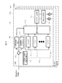
まず、電動機システムについて図1、2を用いて説明する。図1は実施例に係る電動機システムの構成を示すブロック図である。図2は三相モータを示す図である。図3は電力用半導体装置の回路図である。 First, an electric motor system will be described with reference to FIGS. FIG. 1 is a block diagram illustrating a configuration of an electric motor system according to an embodiment. FIG. 2 is a diagram showing a three-phase motor. FIG. 3 is a circuit diagram of the power semiconductor device.
電動機システム1は電動機である三相モータ50と電力用半導体装置を6個用いたインバータ回路30とドライバIC20と制御回路10とトルク指令発生器60と変流器等の電流検出器40と直流電源(不図示)とを備える。インバータ回路30はパワーモジュールともいう。インバータ回路30は、車両等の駆動時には直流電源の電圧から、三相モータ50の各相に電流を流すように、インバータ回路30内部のスイッチングトランジスタ32をON/OFF制御し、このスイッチングの周波数により車両等の速度を変化させる。また、車両等の制動時には、三相モータ50の各相に生じる電圧に同期してスイッチングトランジスタ32をON/OFF制御し、いわゆる整流動作を行い、直流電圧に変換して回生を行う。
The
三相モータ50は回転子が永久磁石で、電機子がコイルで構成され、三相(U相、V相、W相)の電機子巻き線は120度間隔に配置される。コイルはデルタ結線され、常にU相、V相、W相の3つのコイルに電流が流れる。三相モータ50はレゾルバ等の角度検出器51を備える。
In the three-
インバータ回路30は、電力用半導体装置によりU相、V相、W相のブリッジ回路を構成している。U相のブリッジ回路は電力用半導体装置31Uと電力用半導体装置31Xの接続点が三相モータ50に接続されている。V相のブリッジ回路は電力用半導体装置31Vと電力用半導体装置31Yの接続点が三相モータ50に接続されている。W相のブリッジ回路は電力用半導体装置31Wと電力用半導体装置31Zの接続点が三相モータ50に接続されている。ここで、電力用半導体装置31U,31V,31W,31X,31Y,31Zの構成は同じであるので、これらを総称して電力用半導体装置31ということもある。図3に示すように、電力用半導体装置31はIGBTで構成されるスイッチングトランジスタ(以下、IGBTという。)32を備えた半導体チップと、IGBT32のエミッタとコレクタ間に並列に接続された還流ダイオード(FWD)D1を備えた半導体チップとで構成される。還流ダイオードD1は、IGBT32に流れる電流とは逆方向で電流を流すように接続されている。IGBT32と温度検出用ダイオード(不図示)とが形成される半導体チップと還流ダイオードD1が形成される半導体チップとは同一のパッケージに封入するのが好ましい。還流ダイオードD1はIGBT32が形成された半導体チップと同一チップに形成されてもよい。
The
第一半導体装置であるドライバIC20はIGBT32のゲートを駆動する信号を生成する駆動回路(不図示)と過電流検出回路(不図示)と温度検出回路(不図示)を1つの半導体基板に備える。
The
第二半導体装置である制御回路10はCPU11とPWM出力回路12と電流検出回路13と角度検出回路14とメモリ15とを1つの半導体基板(半導体チップ)に備える。CPU11はメモリ15に格納されるソフトウェアに基づいてモータベクトル制御と調整制御とを行う。電流検出回路13は例えばアナログ/デジタル(A/D)変換回路を備える。角度検出回路14は三相モータ50の角度検出器51からの信号を検出するレゾルバ/デジタル(R/D)変換回路を備える。PWM出力回路12はドライバIC20の駆動回路を制御する信号を生成する矩形波生成回路17を備える。メモリ15は上記ソフトウェアの他に後述する基底矩形波情報を格納する。メモリ15はフラッシュメモリ等の不揮発性メモリである。モータベクトル制御および調整制御のソフトウェアと基底矩形波データとは別々の不揮発性メモリに格納してもよい。
The
トルク指令発生器60は、制御回路10の上位に位置し、三相モータ50へのトルク指令を発生する。制御回路10は、トルク指令発生器60のトルク指令に基づき、インバータ回路30を介して三相モータ50の発生トルクを制御する。
The
モータベクトル制御は磁界方向制御(Field Oriented Control:FOC)ともいわれ、静止座標系から回転座標系への変換により交流モータをそれと等価な直流モータとしてモデル化するものである。この交流モータと直流モータの直感的な関係を数学的に対応させるのが回転座標系である。数学的変換を利用すると静止座標系と回転座標系を相互に変換でき、この変換を交流モータのモデルの簡素化に利用できる。数学的変換の一つである順パーク変換(forward Park transformation)は、交流モータの固定子である電機子によって生成すべき磁束を、回転子の回転角の関数として与えるものである。数学的変換の二つ目の逆パーク変換(inverse Park transformation)は、静止座標系における固定子の磁束から、回転座標系の回転子の磁束ベクトルを求めるものである。これら二つの変換を用いて、交流モータの電機子である固定子に関する電流と電圧を直流モータの電機子である回転子に関する電流と電圧に変換することができる。つまり、これによって交流モータの制御モデルを簡単にできる。また、クラーク変換(Clarke transformation)は、三相の各コイルによる磁束を合成してX軸とY軸の直交した成分で表すものである。これによって三相交流モータを制御するのに要する計算処理を二相交流モータに相当する計算処理に削減できることになる。CPU11とメモリ15とを制御部といい、CPU11でモータベクトル制御を行う機能をモータベクトル制御部といい、後述する調整制御を行う機能を調整制御部という。なお、モータベクトル制御部の一部はDSP等の専用プロセッサや専用ハードウェアで実現してもよい。
Motor vector control is also referred to as field-oriented control (FOC), and models an AC motor as an equivalent DC motor by converting from a stationary coordinate system to a rotating coordinate system. The rotational coordinate system mathematically corresponds to the intuitive relationship between the AC motor and the DC motor. When mathematical transformation is used, a stationary coordinate system and a rotational coordinate system can be mutually converted, and this transformation can be used for simplifying the AC motor model. A forward park transformation, which is one of mathematical transformations, gives a magnetic flux to be generated by an armature that is a stator of an AC motor as a function of the rotation angle of the rotor. The second inverse park transformation of mathematical transformation is to obtain the magnetic flux vector of the rotor in the rotating coordinate system from the magnetic flux of the stator in the stationary coordinate system. Using these two conversions, the current and voltage related to the stator that is the armature of the AC motor can be converted into the current and voltage related to the rotor that is the armature of the DC motor. That is, this makes it possible to simplify the control model of the AC motor. In addition, Clark transformation is a combination of magnetic flux generated by three-phase coils and expressed by a component in which the X axis and the Y axis are orthogonal to each other. As a result, the calculation process required to control the three-phase AC motor can be reduced to a calculation process corresponding to the two-phase AC motor. The
次に、図1の矩形波生成回路について図4〜6を用いて説明する。図4は図1の矩形波生成回路を示すブロック図である。図5は図4のコンペア回路を示すブロック図である。図6は矩形波パルスの出力例を説明するためのイメージ図である。 Next, the rectangular wave generation circuit of FIG. 1 will be described with reference to FIGS. FIG. 4 is a block diagram showing the rectangular wave generating circuit of FIG. FIG. 5 is a block diagram showing the compare circuit of FIG. FIG. 6 is an image diagram for explaining an output example of a rectangular wave pulse.
矩形波生成回路17はU相用の矩形波生成回路17UとV相用の矩形波生成回路17V、W相用の矩形波生成回路17Wを備える。U相用の矩形波生成回路17Uはコンペア回路171と、波形合成回路172と、デッドタイム生成回路173と、短パルス除去回路174と、を備える。コンペア回路171は第一コンペア回路171_1、第二コンペア回路171_2、・・・、第nコンペア回路171_nを備える。第一コンペア回路171_1、第二コンペア回路171_2、・・・、第nコンペア回路171_nは同様な構成であり、第nコンペア回路171_nを代表して説明する。
The rectangular
第nコンペア回路171_nは角度を格納する第nレジスタ(REG_Un)1711_nと第n比較器1712_nとを備える。第nレジスタ1711_nはCPU11によって読み出し書き込み可能なレジスタである。第nコンペア回路171_nは第nレジスタ1711_nに格納される角度と角度検出回路14で検出する角度の一致を検出する。第nコンペア回路171_nは角度検出回路14からの角度が第nレジスタ1711_nに格納される角度を超えたことを検出してもよい。
The nth compare circuit 171_n includes an nth register (REG_Un) 1711_n for storing an angle and an nth comparator 1712_n. The nth register 1711_n is a register that can be read and written by the
波形合成回路172は、第一コンペア回路171_1が一致を検出するときHighを出力し、第二コンペア回路171_2が一致を検出するときLowを出力し、第nコンペア回路171_nが一致を検出するときHighを出力する等して矩形波を生成する。第一レジスタ、第二レジスタ、・・・、第nレジスタの値を変更することにより、種々の矩形波を生成することができる。
The
デッドタイム生成回路173は波形合成回路172で生成される矩形波の反転した矩形波を生成し、さらにデットタイムを設けて、これらの矩形波のHigh期間が重ならないようにする。短パルス除去回路174は矩形波のHighの期間が所定期間よりも短いときはそのパルスを除去する。これらにより、U相用の矩形波とU相用の反転した矩形波が生成される。
The dead
矩形波生成回路17は、動作中常にモータの角度情報と基底矩形波データに基づくレジスタ内の角度情報の大小比較を行い、矩形波を生成する。図6に示すように、例えば、U相矩形波は電気角半回転に5パルス出力される。後半の電気角半回転におけるU相矩形波は、前半の電気角半回転におけるU相矩形波に対して反転した波形が出力される。後述する調整は所定の角度範囲(例えば、30度)で位相やデューティを調整する。
The rectangular
V相用の矩形波生成回路17V、W相用の矩形波生成回路17Wは、U相用の矩形波生成回路17Uと同様な構成であるが、矩形波はそれぞれ120度ずれるように生成される。
The V-phase rectangular
次に、矩形波の調整方法いついて図7〜10を用いて説明する。図7は多パルスによる矩形波の調整方法を示すフローチャートである。図8は理論正弦波を算出するフローチャートである。図9は1パルスのモータ電流測定波形を示す図である。図10は矩形波の調整方法を説明するための図である。なお、図9、10では1電気角分の波形が示されている。 Next, a method for adjusting the rectangular wave will be described with reference to FIGS. FIG. 7 is a flowchart showing a rectangular wave adjustment method using multiple pulses. FIG. 8 is a flowchart for calculating a theoretical sine wave. FIG. 9 is a diagram showing a 1-pulse motor current measurement waveform. FIG. 10 is a diagram for explaining a method of adjusting a rectangular wave. 9 and 10 show waveforms for one electrical angle.
モータ電流測定波形が正弦波(理論正弦波)に近づくように、モータを駆動させながら調整する。具体的には以下のように行う。 Adjust while driving the motor so that the motor current measurement waveform approaches a sine wave (theoretical sine wave). Specifically, it is performed as follows.
ステップS1:調整制御部は、図8に示すように、理論正弦波を以下のように算出する。
ステップS11:一定回転にて1回転当たりのモータ電流測定波形と正弦波の偏差テーブルを作成し、ゼロクロスポイントの位相調整を行う。
ステップS12:オフセット調整を行う。
ステップS13:ゲイン調整(合計が0になるよう正弦波のゲインを調整)して理論正弦波を算出する。
Step S1: As shown in FIG. 8, the adjustment control unit calculates a theoretical sine wave as follows.
Step S11: Create a motor current measurement waveform and sine wave deviation table per rotation at a constant rotation, and adjust the phase of the zero cross point.
Step S12: Perform offset adjustment.
Step S13: A theoretical sine wave is calculated by adjusting the gain (adjusting the gain of the sine wave so that the total becomes 0).
ステップS2:調整制御部は、図9に示すように、1パルス時のモータ電流測定波形(1CMW)を測定し、理論正弦波(LSW)との偏差から、基底矩形波を算出する。 Step S2: As shown in FIG. 9, the adjustment control unit measures a motor current measurement waveform (1CMW) at one pulse, and calculates a base rectangular wave from the deviation from the theoretical sine wave (LSW).
ステップS3:調整制御部は、最初は基底矩形波パルスで制御し、モータ1回転に対して十分短い周期でモータ電流を測定し、理論正弦波との差分計算から、調整する。また、調整はパルス数を可変して、理論正弦波に近くパルス数の少ない条件を検索する。例えば、9パルス、7パルス、5パルス、3パルス、1パルス等である。図7ではnパルスのnは9〜1であるがこれに限定されるものではない。 Step S3: The adjustment control unit initially controls with a base rectangular wave pulse, measures the motor current at a sufficiently short period with respect to one rotation of the motor, and adjusts it by calculating the difference from the theoretical sine wave. Further, the adjustment is performed by varying the number of pulses and searching for a condition with a small number of pulses close to a theoretical sine wave. For example, 9 pulses, 7 pulses, 5 pulses, 3 pulses, 1 pulse, etc. In FIG. 7, n of the n pulse is 9 to 1, but is not limited thereto.
ステップS4:調整制御部は、コンペア回路171のレジスタの値を変更することにより、図10に示すように、電流測定波形(CMW)と理論正弦波(LSW)との偏差が最小になるように矩形波パルス(SWP)のデューティ比を調整する。偏差の大きいポイント近くのデューティを可変し、偏差が最小になるよう調整する。なお、本ステップはなくてもよい。
Step S4: The adjustment control unit changes the register value of the compare
ステップS5:調整制御部は、コンペア回路171のレジスタの値を変更することにより、図10に示すように、電流測定波形(CMW)と理論正弦波(LSW)との偏差が最小になるように矩形波パルス(SWP)の位相を調整する。偏差の大きいポイント近くの位相を可変し、偏差が最小になるよう調整する。
Step S5: The adjustment control unit changes the register value of the compare
ステップS6:調整制御部は、コンペア回路171のレジスタの値を変更することにより、図10に示すように、電流測定波形(CMW)と理論正弦波(LSW)との偏差が最小になるように矩形波パルス(SWP)のデューティ比を調整する。
Step S6: The adjustment control unit changes the register value of the compare
ステップS7:調整制御部は、矩形波パルスが最適波形かどうかを判断する。YESの場合は最適な波形のコンペア回路171のレジスタの設定値を基底矩形波情報としてメモリ15に格納して終了し、NOの場合はステップS3に戻る。
Step S7: The adjustment control unit determines whether the rectangular wave pulse is an optimal waveform. If YES, the set value of the register of the optimum waveform compare
これらの調整は、三相モータ50とインバータ回路30をシステム1に組み付けたときに実施するが、負荷状況や、温度依存に応じて動作中に実施しても良い。動作中はメモリ15の基底矩形波情報のデータをコンペア回路171のレジスタに設定して矩形波を生成する。
These adjustments are performed when the three-
次に、発明者が検討した技術(比較例)に係る電動機システムについて図11を用いて説明する。図11は比較例に係る電動機システムの構成を示すブロック図である。 Next, an electric motor system according to a technique (comparative example) studied by the inventors will be described with reference to FIG. FIG. 11 is a block diagram illustrating a configuration of an electric motor system according to a comparative example.
電動機システム1Rは三相モータ50と電力用半導体装置を6個用いたインバータ回路30とドライバIC20と制御回路10Rとトルク指令発生器60と直流電源(不図示)とを備える。制御回路10RはCPU11とPWM出力回路12Rと電流検出回路13と角度検出回路14とメモリ15とを1つの半導体基板に備える。CPU11はメモリ15Rに格納されるソフトウェアに基づいてモータベクトル制御を行う。PWM出力回路12RはドライバIC20の駆動回路を制御する信号を生成する矩形波生成回路17Rを備える。
The
次に、比較例に係る矩形波生成回路について図12を用いて説明する。図12は図11の矩形波生成回路を示すブロック図である。 Next, a rectangular wave generation circuit according to a comparative example will be described with reference to FIG. FIG. 12 is a block diagram showing the rectangular wave generating circuit of FIG.
矩形波生成回路17RはU相用の矩形波生成回路17RUとV相用の矩形波生成回路17RV、W相用の矩形波生成回路17RWを備える。U相用の矩形波生成回路17RUは角度を格納するレジスタ(REG_Un)1711と、比較器1712と、出力設定レジスタ172Rと、デッドタイム生成回路173と、短パルス除去回路174と、を備える。
レジスタ1711および出力設定レジスタ172RはCPU11によって読み出し書き込み可能なレジスタである。比較器1712はレジスタ(REG_Un)1711に格納される角度と角度検出回路14で検出する角度の一致を検出する。
The rectangular
The
矩形波生成回路17Rは、比較器1712が一致を検出するとき割り込み要求を出力し、CPU11の割り込み処理ルーチンにより出力設定レジスタにHighまたはLowが設定されて矩形波が生成される。レジスタ1711および出力設定レジスタ172Rの値を変更することにより、種々の矩形波を生成することができる。しかし、レジスタ1711および出力設定レジスタ172Rの設定値を求める演算および設定、割り込み処理等、CPU11の負荷(制御ソフトウフェアの負荷)が大きい。
The rectangular
V相用の矩形波生成回路17RV、W相用の矩形波生成回路17RWは、U相用の矩形波生成回路17RUと同様な構成であるが、矩形波はそれぞれ120度ずれるように生成される。 The rectangular wave generating circuit 17RV for V phase and the rectangular wave generating circuit 17RW for W phase have the same configuration as the rectangular wave generating circuit 17RU for U phase, but the rectangular waves are generated so as to be shifted by 120 degrees. .
<第一変形例>
次に、第一変形例に係る矩形波生成回路について図13、14を用いて説明する。図13は第一変形例に係る矩形波生成回路を示すブロック図である。図14は矩形波パルスの出力例を説明するためのイメージ図である。第一変形例に係る矩形波生成回路は実施例に係る矩形波生成回路に相毎に進角/遅角を制御する機能を追加したものである。
<First modification>
Next, a rectangular wave generation circuit according to the first modification will be described with reference to FIGS. FIG. 13 is a block diagram showing a rectangular wave generating circuit according to the first modification. FIG. 14 is an image diagram for explaining an output example of a rectangular wave pulse. The rectangular wave generating circuit according to the first modification is obtained by adding a function of controlling the advance angle / retard angle for each phase to the rectangular wave generating circuit according to the embodiment.
矩形波生成回路17AはU相用の矩形波生成回路17AUとV相用の矩形波生成回路17AV、W相用の矩形波生成回路17AWを備える。U相用の矩形波生成回路17AUはコンペア回路171と、波形合成回路172と、デッドタイム生成回路173と、短パルス除去回路174と、相毎に進角/遅角を制御するレジスタ175とレゾルバの角度にレジスタの内容を加算する加算器176と、を備える。レジスタ175はCPU11によって読み出し書き込み可能なレジスタである。
The rectangular
図14に示すように、レジスタ175が進角を設定した場合、U相矩形波は実電気1回転よりも早く出力される。進角遅角制御は、例えば30度毎または数100ns周期で行う。
As shown in FIG. 14, when the
V相用の矩形波生成回路17AV、W相用の矩形波生成回路17AWは、U相用の矩形波生成回路17AUと同様な構成であるが、矩形波はそれぞれ120度ずれるように生成される。 The V-phase rectangular wave generation circuit 17AV and the W-phase rectangular wave generation circuit 17AW have the same configuration as the U-phase rectangular wave generation circuit 17AU, but the rectangular waves are generated so as to be shifted by 120 degrees. .
<第二変形例>
次に、第二変形例に係る矩形波生成回路について図15、16を用いて説明する。図14は第二変形例に係る矩形波生成回路を示すブロック図である。図16は矩形波パルスの出力例を説明するためのイメージ図である。第二変形例に係る矩形波生成回路は第一例に係る矩形波生成回路に正弦波の90度、180度で切り換える機能を追加したものである。
<Second modification>
Next, a rectangular wave generation circuit according to a second modification will be described with reference to FIGS. FIG. 14 is a block diagram showing a rectangular wave generating circuit according to the second modification. FIG. 16 is an image diagram for explaining an output example of a rectangular wave pulse. The rectangular wave generation circuit according to the second modification is obtained by adding a function of switching the sine wave at 90 degrees and 180 degrees to the rectangular wave generation circuit according to the first example.
矩形波生成回路17BはU相用の矩形波生成回路17BUとV相用の矩形波生成回路17BV、W相用の矩形波生成回路17BWを備える。U相用の矩形波生成回路17BUはコンペア回路171Bと、波形合成回路172Bと、デッドタイム生成回路173と、短パルス除去回路174と、相毎に進角/遅角を制御するレジスタ175とレゾルバの角度にレジスタの内容を加算する加算器176と、角度を90度毎にアップ/ダウンする回路177と、180度毎にHigh/Lowを切り替える回路178と、を備える。コンペア回路171Bは第一コンペア回路171_1、第二コンペア回路171_2、・・・、第mコンペア回路171_mを備える。mはnよりも小さく、コンペア回路171Bはコンペア回路171よりもコンペア回路の数は少ない。
The rectangular wave generation circuit 17B includes a rectangular wave generation circuit 17BU for U phase, a rectangular wave generation circuit 17BV for V phase, and a rectangular wave generation circuit 17BW for W phase. The U-phase rectangular wave generation circuit 17BU includes a compare circuit 171B, a
図16に示すように、コンペア回路171Bは正弦波に相当する0〜90度のみ比較する(A)。回路177は比較する角度値を90度毎にアップ/ダウンさせる(B、C、D)。回路178は180度毎に出力のHigh/Lowを切り替える(C、D)。これらにより、残り90〜360度は自動生成することで、コンペア回路171Bおよび波形合成回路172Bの回路規模を削減することができる。
As shown in FIG. 16, the compare circuit 171B compares only 0 to 90 degrees corresponding to a sine wave (A). The
V相用の矩形波生成回路17AV、W相用の矩形波生成回路17AWは、U相用の矩形波生成回路17AUと同様な構成であるが、矩形波はそれぞれ120度ずれるように生成される。 The V-phase rectangular wave generation circuit 17AV and the W-phase rectangular wave generation circuit 17AW have the same configuration as the U-phase rectangular wave generation circuit 17AU, but the rectangular waves are generated so as to be shifted by 120 degrees. .
第二変形例において、実施例と同様に、相毎に進角/遅角を制御するレジスタ175とレゾルバの角度にレジスタの内容を加算する加算器176とはなくてもよい。
In the second modified example, similar to the embodiment, the
<第三変形例>
次に、第三変形例に係る矩形波生成回路について図17、18を用いて説明する。図17は第三変形例に係る矩形波生成回路を示すブロック図である。図18は矩形波パルスの出力例を説明するためのイメージ図である。第三変形例に係る矩形波生成回路は第二変形例に係る矩形波生成回路に三相全体に進角/遅角を制御する機能を追加したものである。
<Third modification>
Next, a rectangular wave generation circuit according to a third modification will be described with reference to FIGS. FIG. 17 is a block diagram showing a rectangular wave generating circuit according to the third modification. FIG. 18 is an image diagram for explaining an output example of a rectangular wave pulse. The rectangular wave generating circuit according to the third modified example is obtained by adding a function of controlling the advance / retarded angle to the entire three phases to the rectangular wave generating circuit according to the second modified example.
矩形波生成回路17CはU相用の矩形波生成回路17BUとV相用の矩形波生成回路17BV、W相用の矩形波生成回路17BWと三相全体に進角/遅角を制御するレジスタ179とレゾルバの角度にレジスタの内容を加算する加算器180とを備える。三相全体を、進角/遅角のため任意のタイミングで位相方向に変更することができる。レジスタ179はCPU11によって読み出し書き込み可能なレジスタである。
The rectangular
図18に示すように、レジスタ179に進角を設定した場合、U相矩形波、V相矩形波およびW相矩形波は実電気1回転よりも早く出力され、レジスタ175に進角を設定した場合、さらにU相矩形波は早く出力される。進角遅角制御は、例えば30度毎または数100ns周期で行う。
As shown in FIG. 18, when the advance angle is set in the
第三変形例において、実施例と同様に、相毎に進角/遅角を制御するレジスタ175とレゾルバの角度にレジスタの内容を加算する加算器176とはなくてもよいし、正弦波の90度、180度で切り換える機能がなくてもよい。
In the third modification, as in the embodiment, the
<第四変形例>
次に、第四変形例に係る矩形波生成回路について図19、20を用いて説明する。図19は第四変形例に係る矩形波生成回路を示すブロック図である。図20は矩形波の生成方法を説明するためのイメージ図である。なお、図16では1電気角分の波形が示されている。第四変形例は理論正弦波に対して一定のヒステリシスを設けた、ヒステリシス制御によりパルス反転位置を指定するものである。
<Fourth modification>
Next, a rectangular wave generation circuit according to a fourth modification will be described with reference to FIGS. FIG. 19 is a block diagram showing a rectangular wave generating circuit according to the fourth modification. FIG. 20 is an image diagram for explaining a method of generating a rectangular wave. FIG. 16 shows a waveform for one electrical angle. In the fourth modification, a pulse inversion position is designated by hysteresis control in which a certain hysteresis is provided for the theoretical sine wave.
矩形波生成回路17DはU相用の矩形波生成回路17DUとV相用の矩形波生成回路17DV、W相用の矩形波生成回路17DWと三相全体に進角/遅角を制御するレジスタ179とレゾルバの角度にレジスタの内容を加算する加算器180とを備える。
The rectangular
U相用の矩形波生成回路17DUは、コンペア上限レジスタ171D1と、コンペア下限レジスタ171D2と、比較回路であるフィルタを含むアナログ比較器172Dと、デッドタイム生成回路173と、短パルス除去回路174と、を備える。U相用の矩形波生成回路17DUは、さらに、相毎に進角/遅角を制御するレジスタ175とレゾルバの角度にレジスタの内容を加算する加算器176と、理論正弦波テーブル177Dと、ゲイン/オフセット調整回路178Dと、減算器17ADと、を備える。コンペア上限レジスタ171D1およびコンペア下限レジスタ171D2はCPU11によって読み出し書き込み可能なメモリである。理論正弦波テーブル177DはCPU11によって読み出し書き込み可能なメモリである。ゲイン/オフセット調整回路178DはCPU11によって読み出し書き込み可能なレジスタを有する。
The U-phase rectangular wave generation circuit 17DU includes a compare upper limit register 171D1, a compare lower limit register 171D2, an
レゾルバの角度(進角または遅角した角度)に対応する理論正弦波テーブル値を理論正弦波テーブル177Dから読み出し、電流検出回路13からのU相電流値と理論正弦波テーブル値との偏差を減算器17ADでU相電流値から理論正弦波テーブル値を減じて算出する。アナログ比較器172Dはこの偏差とコンペア上限レジスタ171D1の値およびコンペア下限レジスタ171D2の値とアナログ比較する。アナログ比較器172Dは偏差が正でありコンペア上限レジスタ171D1の値より大きい場合または等しい場合は矩形波パルス(SWP)をLowにし、偏差が負でありその絶対値がコンペア下限レジスタ171D2の値より大きい場合または等しい場合は矩形波パルス(SWP)をHighにすることで、矩形波パルス(SWP)をOFF/ONする。これにより、理論正弦波に対して一定のヒステリシスを設けることができ、ヒステリシス制御で動作させることができる。ゲイン/オフセット調整回路178DはU相電流値のゲインおよびオフセットを調整し、減算器17ADに供給する。なお、実施例では理想正弦波はゲイン調整やオフセット調整を行って算出しているが、第四変形例では理想正弦波は調整せず、U相電流値をゲイン調整およびオフセット調整を行う。ゲイン調整値およびオフセット調整値は調整工程において取得しメモリ15に格納される。なお、理論正弦波に対して一定のヒステリシスを設けるヒステリシス制御は所定の角度範囲(例えば三相の場合、30度)で動作させても良い。
The theoretical sine wave table value corresponding to the resolver angle (advanced angle or retarded angle) is read from the theoretical sine wave table 177D, and the deviation between the U-phase current value from the
V相用の矩形波生成回路17DV、W相用の矩形波生成回路17DWは、U相用の矩形波生成回路17DUと同様な構成であるが、矩形波はそれぞれ120度ずれるように生成される。 The V-phase rectangular wave generation circuit 17DV and the W-phase rectangular wave generation circuit 17DW have the same configuration as the U-phase rectangular wave generation circuit 17DU, but the rectangular waves are generated so as to be shifted by 120 degrees. .
コンペア上限レジスタ171D1およびコンペア下限レジスタの設定によって矩形波が調整可能である。 The rectangular wave can be adjusted by setting the compare upper limit register 171D1 and the compare lower limit register.
第四変形例は実施例よりも矩形波のパルス数は増える可能性あるが、理論正弦波に近づけられる可能性あり、効率が良くなる場合もある。 In the fourth modified example, the number of pulses of the rectangular wave may be increased as compared with the embodiment, but it may be approximated to a theoretical sine wave, and the efficiency may be improved.
実施例、第一乃至第四変形例によれば、多パルスを出力するためのソフトウェアが不要となり、ソフトウェア負荷を改善(低減)することができる。 According to the embodiment and the first to fourth modified examples, software for outputting multiple pulses becomes unnecessary, and the software load can be improved (reduced).
比較例では、ソフトウェアでタイミングを合わせて、矩形波出力のU/V/W各相を非同期で個別に切り替える必要があり、切替が競合する場合、いずれかの相に遅延が生じ波形に影響するが、実施例、第一乃至第四変形例では、この問題を改善することができる。また、比較例では、多パルスのパルス幅間隔が狭い場合、ソフトウェアによる処理が追いつかず期待の出力が得られないが、実施例、第一乃至第四変形例では、この問題を改善することができる。 In the comparative example, it is necessary to switch each phase of the rectangular wave output U / V / W asynchronously and individually by matching the timing with software. When switching conflicts, a delay occurs in one of the phases and the waveform is affected. However, this problem can be improved in the embodiment and the first to fourth modifications. Further, in the comparative example, when the pulse width interval of multiple pulses is narrow, the processing by software cannot catch up and an expected output cannot be obtained, but this problem can be improved in the examples and the first to fourth modified examples. it can.
比較例では、多パルスのパルス数が多い場合、ソフトウェアの負荷が増大し、切替に間に合わない場合が発生し、最悪、1電気角回転の期間、出力できない問題が発生するので、安全確保のため、切替が抜けたことを検出する機能の追加と、さらなるソフトウェア負荷が追加となるが、実施例、第一乃至第四変形例では、この問題を改善することができる。 In the comparative example, when the number of multi-pulses is large, the software load increases, and there are cases where it is not in time for switching, and in the worst case, there is a problem that it cannot be output for one electrical angle rotation period. Although the addition of a function for detecting that the switching has been lost and the additional software load are added, this problem can be improved in the embodiment and the first to fourth modifications.
実施例、第一乃至第四変形例では、角度や速度、温度に応じて異なる矩形波パルスの出力パターンを個々の三相モータでキャリブレーションすることができる。 In the embodiment and the first to fourth modifications, output patterns of different rectangular wave pulses depending on the angle, speed, and temperature can be calibrated by individual three-phase motors.
以上、本発明者によってなされた発明を実施例および変形例に基づき具体的に説明したが、本発明は、上記実施例および変形例に限定されるものではなく、種々変更可能であることはいうまでもない。 As mentioned above, the invention made by the present inventor has been specifically described based on the embodiments and the modified examples. However, the present invention is not limited to the above-described embodiments and modified examples, and various modifications can be made. Not too long.
例えば、実施例および変形例では三相モータを使用する場合について説明したが、これに限定されるものではなく、二相モータや四相以上の多相モータに適用することができる。 For example, although a case where a three-phase motor is used has been described in the embodiments and modifications, the present invention is not limited to this, and can be applied to a two-phase motor or a four-phase or more multi-phase motor.
1・・・電動機システム
10・・・制御回路
11・・・CPU
12・・・PWM出力回路
13・・・電流検出回路
14・・・角度検出回路
15・・・メモリ
17・・・矩形波生成回路
171・・・コンペア回路
172・・・矩形波合成回路
173・・・デッドタイム生成回路
174・・・短パルス除去回路
20・・・ドライバIC
30・・・インバータ回路
40・・・電流検出器
50・・・三相モータ
DESCRIPTION OF
12 ...
30 ...
Claims (18)
CPUとメモリを含む制御部と、
電力用半導体装置を駆動するドライバICを制御するPWM出力回路と、
モータ電流を検出する電流検出回路と、
モータの角度を検出する角度検出回路と、
を備え、
前記PWM出力回路は矩形波生成回路を備え、
前記矩形波生成回路は前記角度検出回路の角度情報と基底矩形波情報とに基づいて矩形波を生成する。 Semiconductor devices
A control unit including a CPU and a memory;
A PWM output circuit that controls a driver IC that drives the power semiconductor device;
A current detection circuit for detecting the motor current;
An angle detection circuit for detecting the angle of the motor;
With
The PWM output circuit includes a rectangular wave generation circuit,
The rectangular wave generation circuit generates a rectangular wave based on the angle information of the angle detection circuit and the base rectangular wave information.
前記矩形波生成回路は、
前記角度検出回路からの角度情報と前記基底矩形波情報に基づいて設定されたレジスタ内の角度情報とを比較するコンペア回路と、
前記コンペア回路の比較結果に基づいて矩形波パルスの立上げまたは立ち下げを行う波形合成回路と、
を備える。 The semiconductor device according to claim 1.
The rectangular wave generation circuit includes:
A compare circuit that compares angle information from the angle detection circuit and angle information in a register set based on the base rectangular wave information;
A waveform synthesis circuit for raising or lowering a rectangular wave pulse based on the comparison result of the compare circuit;
Is provided.
前記メモリは前記基底矩形波情報を格納する。 The semiconductor device according to claim 2.
The memory stores the base rectangular wave information.
前記基底矩形波情報は理論正弦波とモータ電流測定波形の偏差に基づいて算出される。 The semiconductor device according to claim 3.
The base rectangular wave information is calculated based on the deviation between the theoretical sine wave and the motor current measurement waveform.
前記基底矩形波情報は前記偏差が最小になるように矩形波パルスのデューティ比および位相を調整して算出される。 The semiconductor device according to claim 4.
The base rectangular wave information is calculated by adjusting the duty ratio and phase of the rectangular wave pulse so that the deviation is minimized.
前記制御部は、
理論正弦波を算出する手段と、
1パルスによるモータ電流測定波形と前記理論正弦波との偏差に基づいて前記基底矩形波情報を算出する手段と、
前記基底矩形波情報のデューティ比を変えて調整する手段と、
前記基底矩形波情報の位相を変えて調整する手段と、
調整した基底矩形波情報を前記メモリに格納する手段と、
を備える。 The semiconductor device according to claim 1.
The controller is
Means for calculating a theoretical sine wave;
Means for calculating the base rectangular wave information based on a deviation between a motor current measurement waveform by one pulse and the theoretical sine wave;
Means for changing and adjusting the duty ratio of the base rectangular wave information;
Means for changing and adjusting the phase of the base rectangular wave information;
Means for storing adjusted basis rectangular wave information in the memory;
Is provided.
前記制御部は、さらにモータベクトル制御手段を備える。 The semiconductor device according to claim 6.
The control unit further includes motor vector control means.
電力用半導体装置を駆動するドライバICを制御するPWM出力回路と、
モータ電流を検出する電流検出回路と、
モータの角度を検出する角度検出回路と、
を備え、
前記PWM出力回路は矩形波生成回路を備え、
前記矩形波生成回路は前記角度検出回路の角度情報と理論正弦波とに基づいて矩形波を生成する。 Semiconductor devices
A PWM output circuit that controls a driver IC that drives the power semiconductor device;
A current detection circuit for detecting the motor current;
An angle detection circuit for detecting the angle of the motor;
With
The PWM output circuit includes a rectangular wave generation circuit,
The rectangular wave generation circuit generates a rectangular wave based on angle information of the angle detection circuit and a theoretical sine wave.
前記矩形波生成回路は、
前記角度検出回路からの角度情報に対応する電流情報を格納する理論正弦波テーブルと、
前記電流検出回路からの電流情報と前記理論正弦波テーブルの電流情報との偏差を求める演算器と、
前記偏差の上限を設定する上限レジスタと、
前記偏差の下限を設定する下限レジスタと、
前記偏差と前記上限レジスタの内容の比較結果および前記偏差と前記下限レジスタの内容の比較結果に基づいて矩形波パルスの立上げまたは立ち下げを行う比較回路と、
を備える。 The semiconductor device according to claim 8.
The rectangular wave generation circuit includes:
A theoretical sine wave table for storing current information corresponding to angle information from the angle detection circuit;
A calculator for obtaining a deviation between the current information from the current detection circuit and the current information of the theoretical sine wave table;
An upper limit register for setting the upper limit of the deviation;
A lower limit register for setting the lower limit of the deviation;
A comparison circuit that rises or falls a rectangular wave pulse based on a comparison result between the deviation and the contents of the upper limit register and a comparison result between the deviation and the contents of the lower limit register;
Is provided.
前記比較回路は、前記偏差が前記上限レジスタの値以上または超えた場合は矩形波パルスを立下げ、前記偏差が前記下限レジスタの値以下または下回った場合は矩形波パルスを立上げる。 The semiconductor device according to claim 9.
The comparison circuit causes the rectangular wave pulse to fall when the deviation exceeds or exceeds the value of the upper limit register, and raises the rectangular wave pulse when the deviation falls below or below the value of the lower limit register.
前記矩形波生成回路は、さらに、前記電流検出回路からの電流情報のゲインおよびオフセットを調整する回路を備える。 The semiconductor device according to claim 10.
The rectangular wave generation circuit further includes a circuit that adjusts the gain and offset of current information from the current detection circuit.
電動機に交流電流を供給する電力用半導体装置と、
前記電力用半導体装置を駆動する第一半導体装置と、
前記第一半導体装置を制御する第二半導体装置と、
前記電動機の電流を検出する電流検出器と、
前記電動機の角度を検出する角度検出器と、
を備え、
前記第二半導体装置は、
CPUとメモリを含む制御部と、
前記第一半導体装置を制御するPWM出力回路と、
前記電流検出器からの電流情報を検出する電流検出回路と、
前記角度検出器からの角度情報を検出する角度検出回路と、
を備え、
前記PWM出力回路は矩形波生成回路を備え、
前記矩形波生成回路は前記角度検出回路の角度情報と基底矩形波情報とに基づいて矩形波を生成する。 Power conversion device
A power semiconductor device for supplying an alternating current to an electric motor;
A first semiconductor device for driving the power semiconductor device;
A second semiconductor device for controlling the first semiconductor device;
A current detector for detecting the current of the motor;
An angle detector for detecting the angle of the electric motor;
With
The second semiconductor device is
A control unit including a CPU and a memory;
A PWM output circuit for controlling the first semiconductor device;
A current detection circuit for detecting current information from the current detector;
An angle detection circuit for detecting angle information from the angle detector;
With
The PWM output circuit includes a rectangular wave generation circuit,
The rectangular wave generation circuit generates a rectangular wave based on the angle information of the angle detection circuit and the base rectangular wave information.
前記矩形波生成回路は、
前記角度検出回路からの角度情報と前記基底矩形波情報に基づいて設定されたレジスタ内の角度情報とを比較するコンペア回路と、
前記コンペア回路の比較結果に基づいて矩形波パルスの立上げまたは立ち下げを行う波形合成回路と、
を備える。 The power converter of claim 12,
The rectangular wave generation circuit includes:
A compare circuit that compares angle information from the angle detection circuit and angle information in a register set based on the base rectangular wave information;
A waveform synthesis circuit for raising or lowering a rectangular wave pulse based on the comparison result of the compare circuit;
Is provided.
前記メモリは前記基底矩形波情報を格納する。 The power converter of claim 13,
The memory stores the base rectangular wave information.
前記基底矩形波情報は理論正弦波とモータ電流測定波形の偏差に基づいて算出される。 The power converter of claim 14,
The base rectangular wave information is calculated based on the deviation between the theoretical sine wave and the motor current measurement waveform.
前記基底矩形波情報は前記偏差が最小になるように矩形波パルスのデューティ比および位相を調整して算出される。 The power converter of claim 15,
The base rectangular wave information is calculated by adjusting the duty ratio and phase of the rectangular wave pulse so that the deviation is minimized.
前記制御部は、
理論正弦波を算出する手段と、
1パルスによるモータ電流測定波形と前記理論正弦波との偏差に基づいて前記基底矩形波情報を算出する手段と、
前記基底矩形波情報のデューティ比を変えて調整する手段と、
前記基底矩形波情報の位相を変えて調整する手段と、
調整した基底矩形波情報を前記メモリに格納する手段と、
を備える。 The power converter of claim 12,
The controller is
Means for calculating a theoretical sine wave;
Means for calculating the base rectangular wave information based on a deviation between a motor current measurement waveform by one pulse and the theoretical sine wave;
Means for changing and adjusting the duty ratio of the base rectangular wave information;
Means for changing and adjusting the phase of the base rectangular wave information;
Means for storing adjusted basis rectangular wave information in the memory;
Is provided.
前記制御部は、さらにモータベクトル制御手段を備える。 The power converter of claim 17,
The control unit further includes motor vector control means.
Priority Applications (5)
| Application Number | Priority Date | Filing Date | Title |
|---|---|---|---|
| JP2016255581A JP2018107996A (en) | 2016-12-28 | 2016-12-28 | Semiconductor device and power conversion device |
| US15/814,213 US10312850B2 (en) | 2016-12-28 | 2017-11-15 | Semiconductor device and power conversion device |
| EP17208363.6A EP3343758B1 (en) | 2016-12-28 | 2017-12-19 | Semiconductor device and power conversion device |
| KR1020170179471A KR20180077057A (en) | 2016-12-28 | 2017-12-26 | Semiconductor device and power conversion device |
| CN201711455155.4A CN108258975B (en) | 2016-12-28 | 2017-12-28 | Semiconductor device and power conversion device |
Applications Claiming Priority (1)
| Application Number | Priority Date | Filing Date | Title |
|---|---|---|---|
| JP2016255581A JP2018107996A (en) | 2016-12-28 | 2016-12-28 | Semiconductor device and power conversion device |
Publications (1)
| Publication Number | Publication Date |
|---|---|
| JP2018107996A true JP2018107996A (en) | 2018-07-05 |
Family
ID=60673954
Family Applications (1)
| Application Number | Title | Priority Date | Filing Date |
|---|---|---|---|
| JP2016255581A Pending JP2018107996A (en) | 2016-12-28 | 2016-12-28 | Semiconductor device and power conversion device |
Country Status (5)
| Country | Link |
|---|---|
| US (1) | US10312850B2 (en) |
| EP (1) | EP3343758B1 (en) |
| JP (1) | JP2018107996A (en) |
| KR (1) | KR20180077057A (en) |
| CN (1) | CN108258975B (en) |
Cited By (1)
| Publication number | Priority date | Publication date | Assignee | Title |
|---|---|---|---|---|
| CN113424129A (en) * | 2019-02-07 | 2021-09-21 | 弗雷亚尔食品有限公司 | Motor control circuit with power factor correction |
Families Citing this family (5)
| Publication number | Priority date | Publication date | Assignee | Title |
|---|---|---|---|---|
| US10913550B2 (en) | 2018-03-23 | 2021-02-09 | The Boeing Company | System and method for position and speed feedback control |
| US10830591B2 (en) | 2018-03-23 | 2020-11-10 | The Boeing Company | System and method for dual speed resolver |
| US10911061B2 (en) * | 2018-03-23 | 2021-02-02 | The Boeing Company | System and method for demodulation of resolver outputs |
| CN112567620B (en) * | 2018-08-30 | 2024-03-01 | 日立安斯泰莫株式会社 | Inverter device |
| KR102881916B1 (en) * | 2019-08-01 | 2025-11-05 | 현대자동차주식회사 | Overcurrent detection reference compensation system of switching element for inverter and overcurrent detection system using the same |
Citations (2)
| Publication number | Priority date | Publication date | Assignee | Title |
|---|---|---|---|---|
| JP2008220034A (en) * | 2007-03-02 | 2008-09-18 | Denso Corp | Rotating machine control device |
| JP2011035991A (en) * | 2009-07-30 | 2011-02-17 | Hitachi Automotive Systems Ltd | Power conversion device |
Family Cites Families (11)
| Publication number | Priority date | Publication date | Assignee | Title |
|---|---|---|---|---|
| US4649467A (en) * | 1985-07-31 | 1987-03-10 | United Technologies Corporation | High efficiency MOSFET sine wave generator |
| JP2008092784A (en) * | 2006-07-28 | 2008-04-17 | Mitsuba Corp | Drive unit for brushless motor, and method for starting the brushless motor and method for detecting stopping position of rotor of the brushless motor |
| JP5609051B2 (en) * | 2009-09-18 | 2014-10-22 | トヨタ自動車株式会社 | Three-phase AC motor drive controller |
| WO2011135696A1 (en) * | 2010-04-28 | 2011-11-03 | 株式会社 日立製作所 | Power conversion device |
| JP5741966B2 (en) * | 2012-12-03 | 2015-07-01 | 株式会社デンソー | AC motor control device |
| US20140327379A1 (en) * | 2013-05-03 | 2014-11-06 | Texas Instruments Incorporated | Position sensorless drive system and method for permanent magnet motors |
| JP5920635B2 (en) * | 2013-08-20 | 2016-05-18 | 株式会社デンソー | AC motor control device |
| JP5910583B2 (en) * | 2013-08-20 | 2016-04-27 | 株式会社デンソー | AC motor control device |
| JP6204121B2 (en) | 2013-09-09 | 2017-09-27 | 株式会社日立製作所 | Motor drive system and electric railway vehicle equipped with the system |
| JP6406108B2 (en) * | 2015-04-15 | 2018-10-17 | 株式会社デンソー | Control device for motor control system |
| CN105576993B (en) * | 2016-01-12 | 2018-05-29 | 永大电梯设备(中国)有限公司 | A kind of frequency converter dead-time compensation method and compensation system |
-
2016
- 2016-12-28 JP JP2016255581A patent/JP2018107996A/en active Pending
-
2017
- 2017-11-15 US US15/814,213 patent/US10312850B2/en active Active
- 2017-12-19 EP EP17208363.6A patent/EP3343758B1/en active Active
- 2017-12-26 KR KR1020170179471A patent/KR20180077057A/en not_active Withdrawn
- 2017-12-28 CN CN201711455155.4A patent/CN108258975B/en active Active
Patent Citations (2)
| Publication number | Priority date | Publication date | Assignee | Title |
|---|---|---|---|---|
| JP2008220034A (en) * | 2007-03-02 | 2008-09-18 | Denso Corp | Rotating machine control device |
| JP2011035991A (en) * | 2009-07-30 | 2011-02-17 | Hitachi Automotive Systems Ltd | Power conversion device |
Cited By (1)
| Publication number | Priority date | Publication date | Assignee | Title |
|---|---|---|---|---|
| CN113424129A (en) * | 2019-02-07 | 2021-09-21 | 弗雷亚尔食品有限公司 | Motor control circuit with power factor correction |
Also Published As
| Publication number | Publication date |
|---|---|
| EP3343758A1 (en) | 2018-07-04 |
| CN108258975B (en) | 2023-05-16 |
| CN108258975A (en) | 2018-07-06 |
| US20180183378A1 (en) | 2018-06-28 |
| EP3343758B1 (en) | 2020-11-11 |
| KR20180077057A (en) | 2018-07-06 |
| US10312850B2 (en) | 2019-06-04 |
Similar Documents
| Publication | Publication Date | Title |
|---|---|---|
| EP3343758B1 (en) | Semiconductor device and power conversion device | |
| US7075267B1 (en) | Space vector-based current controlled PWM inverter for motor drives | |
| CN102545763B (en) | Methods, systems and apparatus for adjusting duty cycle of pulse width modulated (PWM) waveforms | |
| US8278865B2 (en) | Control device | |
| US8232753B2 (en) | Control device for electric motor drive apparatus | |
| US9871483B2 (en) | Controller for rotary electric machine drive apparatus | |
| JP4749874B2 (en) | Power conversion device and motor drive device using the same | |
| JP4575547B2 (en) | Motor control device | |
| US11705841B2 (en) | Estimation device and AC motor drive device | |
| CN108966683B (en) | Inverter control device | |
| CN104638964A (en) | Method for driving power conversion system, power conversion system, and switch controller | |
| CN113826317B (en) | Control device for rotating electrical machine | |
| JP2009232604A (en) | Rotating electric machine control system | |
| CN108633323B (en) | Power conversion device and rotary electric machine drive device | |
| JP6579195B2 (en) | Power control method and power control apparatus | |
| JP2012157103A (en) | Inverter device, fan drive device, compressor drive device and air conditioner | |
| JP4722002B2 (en) | PWM inverter control device, PWM inverter control method, and refrigeration air conditioner | |
| CN113039717A (en) | AC rotating machine control device | |
| JP6471670B2 (en) | Power control method and power control apparatus | |
| JP2000152683A (en) | Method for controlling brushless dc motor | |
| US12095373B2 (en) | Power conversion apparatus | |
| US20250158549A1 (en) | Motor drive system and corresponding method | |
| JP2019213284A (en) | Motor controller, control method and program thereof |
Legal Events
| Date | Code | Title | Description |
|---|---|---|---|
| A621 | Written request for application examination |
Free format text: JAPANESE INTERMEDIATE CODE: A621 Effective date: 20190408 |
|
| A977 | Report on retrieval |
Free format text: JAPANESE INTERMEDIATE CODE: A971007 Effective date: 20200213 |
|
| A131 | Notification of reasons for refusal |
Free format text: JAPANESE INTERMEDIATE CODE: A131 Effective date: 20200324 |
|
| A02 | Decision of refusal |
Free format text: JAPANESE INTERMEDIATE CODE: A02 Effective date: 20201006 |