JP2016114779A - Liquid crystal display device - Google Patents

Liquid crystal display device Download PDF

Info

Publication number
JP2016114779A
JP2016114779A JP2014253260A JP2014253260A JP2016114779A JP 2016114779 A JP2016114779 A JP 2016114779A JP 2014253260 A JP2014253260 A JP 2014253260A JP 2014253260 A JP2014253260 A JP 2014253260A JP 2016114779 A JP2016114779 A JP 2016114779A
Authority
JP
Japan
Prior art keywords
liquid crystal
display device
crystal display
insulating layer
signal line
Prior art date
Legal status (The legal status is an assumption and is not a legal conclusion. Google has not performed a legal analysis and makes no representation as to the accuracy of the status listed.)
Pending
Application number
JP2014253260A
Other languages
Japanese (ja)
Inventor
伊東 理
Osamu Ito
理 伊東
中尾 健次
Kenji Nakao
健次 中尾
利昌 石垣
Toshimasa Ishigaki
利昌 石垣
小菅 将洋
Masahiro Kosuge
将洋 小菅
Current Assignee (The listed assignees may be inaccurate. Google has not performed a legal analysis and makes no representation or warranty as to the accuracy of the list.)
Japan Display Inc
Original Assignee
Japan Display Inc
Priority date (The priority date is an assumption and is not a legal conclusion. Google has not performed a legal analysis and makes no representation as to the accuracy of the date listed.)
Filing date
Publication date
Application filed by Japan Display Inc filed Critical Japan Display Inc
Priority to JP2014253260A priority Critical patent/JP2016114779A/en
Priority to CN201521005674.7U priority patent/CN205353531U/en
Priority to US14/967,868 priority patent/US9690131B2/en
Publication of JP2016114779A publication Critical patent/JP2016114779A/en
Pending legal-status Critical Current

Links

Images

Classifications

    • GPHYSICS
    • G02OPTICS
    • G02FOPTICAL DEVICES OR ARRANGEMENTS FOR THE CONTROL OF LIGHT BY MODIFICATION OF THE OPTICAL PROPERTIES OF THE MEDIA OF THE ELEMENTS INVOLVED THEREIN; NON-LINEAR OPTICS; FREQUENCY-CHANGING OF LIGHT; OPTICAL LOGIC ELEMENTS; OPTICAL ANALOGUE/DIGITAL CONVERTERS
    • G02F1/00Devices or arrangements for the control of the intensity, colour, phase, polarisation or direction of light arriving from an independent light source, e.g. switching, gating or modulating; Non-linear optics
    • G02F1/01Devices or arrangements for the control of the intensity, colour, phase, polarisation or direction of light arriving from an independent light source, e.g. switching, gating or modulating; Non-linear optics for the control of the intensity, phase, polarisation or colour 
    • G02F1/13Devices or arrangements for the control of the intensity, colour, phase, polarisation or direction of light arriving from an independent light source, e.g. switching, gating or modulating; Non-linear optics for the control of the intensity, phase, polarisation or colour  based on liquid crystals, e.g. single liquid crystal display cells
    • G02F1/133Constructional arrangements; Operation of liquid crystal cells; Circuit arrangements
    • G02F1/1333Constructional arrangements; Manufacturing methods
    • G02F1/1335Structural association of cells with optical devices, e.g. polarisers or reflectors
    • G02F1/133502Antiglare, refractive index matching layers
    • GPHYSICS
    • G02OPTICS
    • G02FOPTICAL DEVICES OR ARRANGEMENTS FOR THE CONTROL OF LIGHT BY MODIFICATION OF THE OPTICAL PROPERTIES OF THE MEDIA OF THE ELEMENTS INVOLVED THEREIN; NON-LINEAR OPTICS; FREQUENCY-CHANGING OF LIGHT; OPTICAL LOGIC ELEMENTS; OPTICAL ANALOGUE/DIGITAL CONVERTERS
    • G02F1/00Devices or arrangements for the control of the intensity, colour, phase, polarisation or direction of light arriving from an independent light source, e.g. switching, gating or modulating; Non-linear optics
    • G02F1/01Devices or arrangements for the control of the intensity, colour, phase, polarisation or direction of light arriving from an independent light source, e.g. switching, gating or modulating; Non-linear optics for the control of the intensity, phase, polarisation or colour 
    • G02F1/13Devices or arrangements for the control of the intensity, colour, phase, polarisation or direction of light arriving from an independent light source, e.g. switching, gating or modulating; Non-linear optics for the control of the intensity, phase, polarisation or colour  based on liquid crystals, e.g. single liquid crystal display cells
    • G02F1/133Constructional arrangements; Operation of liquid crystal cells; Circuit arrangements
    • G02F1/136Liquid crystal cells structurally associated with a semi-conducting layer or substrate, e.g. cells forming part of an integrated circuit
    • G02F1/1362Active matrix addressed cells
    • G02F1/136286Wiring, e.g. gate line, drain line

Landscapes

  • Physics & Mathematics (AREA)
  • Nonlinear Science (AREA)
  • Mathematical Physics (AREA)
  • Chemical & Material Sciences (AREA)
  • Crystallography & Structural Chemistry (AREA)
  • General Physics & Mathematics (AREA)
  • Optics & Photonics (AREA)
  • Liquid Crystal (AREA)
  • Engineering & Computer Science (AREA)
  • Microelectronics & Electronic Packaging (AREA)

Abstract

【課題】カラーフィルタが液晶層に溶出することを抑制する。【解決手段】能動素子基板、前記能動素子基板の上に設けられた液晶層400、及び前記液晶層400の上に設けられた対向基板を備える液晶表示装置であって、前記能動素子基板は、能動素子と、共通電極95と、前記共通電極95と電気的に接続している共通配線4と、前記共通配線4上に設けられた反射抑制膜5と、前記反射抑制膜5上に設けられた第1絶縁層3と、前記第1絶縁層3上に設けられた板状部、及び下方に突出した第1突出部を有する画素電極と、を備え、前記第1突出部は、前記能動素子と電気的に接続している液晶表示装置。【選択図】図3A color filter is prevented from being eluted into a liquid crystal layer. A liquid crystal display device comprising an active element substrate, a liquid crystal layer 400 provided on the active element substrate, and a counter substrate provided on the liquid crystal layer 400, wherein the active element substrate includes: An active element, a common electrode 95, a common wiring 4 electrically connected to the common electrode 95, a reflection suppressing film 5 provided on the common wiring 4, and provided on the reflection suppressing film 5 And a pixel electrode having a plate-like portion provided on the first insulating layer 3 and a first protruding portion protruding downward, wherein the first protruding portion is the active portion. A liquid crystal display device electrically connected to the element. [Selection] Figure 3

Description

本発明は液晶表示装置に関し、特にカラーフィルタと能動素子とを同じ基板側に配置した液晶表示装置に関する。   The present invention relates to a liquid crystal display device, and more particularly to a liquid crystal display device in which a color filter and an active element are arranged on the same substrate side.

液晶を介して上側の基板にカラーフィルタ及びブラックマトリクスを設け、下側の基板に配線及び能動素子を設けた液晶表示装置は、位置を合わせることが非常に難しく、混色及び開口率の低下を生じやすい。こうした問題を解消するため、カラーフィルタ及び能動素子を同一基板上に形成したCOA(Color filter On Array)方式が用いられている。 A liquid crystal display device in which a color filter and a black matrix are provided on the upper substrate via a liquid crystal and wiring and active elements are provided on the lower substrate is very difficult to align, resulting in color mixing and a decrease in aperture ratio. Cheap. In order to solve such problems, a COA (Color filter On Array) system in which a color filter and an active element are formed on the same substrate is used.

特許文献1には、一方の基板において、能動素子の保護膜上にカラーフィルタを設け、カラーフィルタおよび能動素子の保護膜にコンタクトホールを形成することによって能動素子の画素電極と画素電極とを接続する表示装置が記載されている。   In Patent Document 1, a color filter is provided on a protective film of an active element on one substrate, and a contact hole is formed in the protective film of the color filter and the active element to connect the pixel electrode and the pixel electrode of the active element. A display device is described.

特開2002−350886号公報JP 2002-350886 A

一方、液晶表示装置には、能動素子が設けられた能動素子基板に共通電極が設けられている。また、共通電極の電位を一定にするため、共通電極より低抵抗の共通配線が設けられることがある。 On the other hand, in the liquid crystal display device, a common electrode is provided on an active element substrate on which an active element is provided. In order to keep the potential of the common electrode constant, a common wiring having a lower resistance than the common electrode may be provided.

FFS(Fringe Field Switching)方式を含むIPS(In Plane Switching)方式の場合、能動素子を備える能動素子基板に共通電極及び共通配線が設けられる。また、COA方式においては、カラーフィルタの上方に共通電極及び共通配線が設けられるところ、特に共通配線が上方からの外光を反射した場合に、液晶表示装置のコントラスト比が低下するという課題があった。   In the case of an IPS (In Plane Switching) system including an FFS (Fringe Field Switching) system, a common electrode and a common wiring are provided on an active element substrate including an active element. In the COA method, a common electrode and a common wiring are provided above the color filter. In particular, when the common wiring reflects external light from above, there is a problem that the contrast ratio of the liquid crystal display device is lowered. It was.

本発明は、かかる課題を解決するものであり、共通配線上に反射抑制膜が設けられた液晶表示装置を提供する。   The present invention solves this problem and provides a liquid crystal display device in which a reflection suppressing film is provided on a common wiring.

本発明の液晶表示装置は、第1基板、前記第1基板上に設けられた液晶層、及び前記液晶層上に設けられた第2基板を備える液晶表示装置であって、前記第1基板は、カラーフィルタと、前記カラーフィルタ上に設けられた共通電極と、前記共通電極と電気的に接続している共通配線と、前記共通配線上及び前記カラーフィルタ上に設けられた反射抑制膜と、前記共通電極との間に電界を発生させる画素電極と、前記共通電極及び前記画素電極の間に設けられた第1絶縁層と、を備える。   The liquid crystal display device of the present invention is a liquid crystal display device comprising a first substrate, a liquid crystal layer provided on the first substrate, and a second substrate provided on the liquid crystal layer, wherein the first substrate is A color filter, a common electrode provided on the color filter, a common wiring electrically connected to the common electrode, a reflection suppressing film provided on the common wiring and the color filter, A pixel electrode that generates an electric field between the common electrode and a first insulating layer provided between the common electrode and the pixel electrode;

本発明によれば 共通配線上に反射抑制膜が設けられているので、外光下においてもコントラスト比の低下を抑制することができる。   According to the present invention, since the antireflection film is provided on the common wiring, it is possible to suppress a decrease in contrast ratio even under external light.

実施形態1における液晶表示装置の斜視図である。1 is a perspective view of a liquid crystal display device in Embodiment 1. FIG. 実施形態1における能動素子基板の平面図である。3 is a plan view of an active element substrate in Embodiment 1. FIG. 実施形態1における液晶表示装置の断面図である。1 is a cross-sectional view of a liquid crystal display device in Embodiment 1. FIG. 実施形態1における液晶表示装置の断面図である。1 is a cross-sectional view of a liquid crystal display device in Embodiment 1. FIG. 実施形態1における能動素子基板の平面図である。3 is a plan view of an active element substrate in Embodiment 1. FIG. 実施形態1における能動素子基板の平面図である。3 is a plan view of an active element substrate in Embodiment 1. FIG. 実施形態1における能動素子基板の平面図である。3 is a plan view of an active element substrate in Embodiment 1. FIG. 実施形態2における液晶表示装置の断面図である。6 is a cross-sectional view of a liquid crystal display device according to Embodiment 2. FIG. 実施形態2における液晶表示装置の断面図である。6 is a cross-sectional view of a liquid crystal display device according to Embodiment 2. FIG. 実施形態3における液晶表示装置100の断面図である。6 is a cross-sectional view of a liquid crystal display device 100 according to Embodiment 3. FIG. 実施形態3における液晶表示装置100の断面図である。6 is a cross-sectional view of a liquid crystal display device 100 according to Embodiment 3. FIG. 実施形態4における液晶表示装置の断面図である。6 is a cross-sectional view of a liquid crystal display device in Embodiment 4. FIG. 実施形態4における液晶表示装置の断面図である。6 is a cross-sectional view of a liquid crystal display device in Embodiment 4. FIG. 実施形態5における液晶表示装置の断面図である。6 is a cross-sectional view of a liquid crystal display device in Embodiment 5. FIG. 実施形態5における液晶表示装置の断面図である。6 is a cross-sectional view of a liquid crystal display device in Embodiment 5. FIG. 実施形態5における能動素子基板の平面図である。10 is a plan view of an active element substrate in Embodiment 5. FIG. 実施形態6における液晶表示装置の製造方法を示す図である。It is a figure which shows the manufacturing method of the liquid crystal display device in Embodiment 6. FIG. 実施形態6における液晶表示装置の製造方法を示す図である。It is a figure which shows the manufacturing method of the liquid crystal display device in Embodiment 6. FIG. 実施形態7における液晶表示装置の断面図である。10 is a cross-sectional view of a liquid crystal display device in Embodiment 7. FIG. 実施形態7における液晶表示装置の断面図である。10 is a cross-sectional view of a liquid crystal display device in Embodiment 7. FIG. 実施形態7における能動素子基板の平面図である。FIG. 10 is a plan view of an active element substrate in a seventh embodiment. 実施形態8における液晶表示装置の断面図である。10 is a cross-sectional view of a liquid crystal display device in Embodiment 8. FIG. 実施形態8における液晶表示装置の断面図である。10 is a cross-sectional view of a liquid crystal display device in Embodiment 8. FIG. 実施形態9における液晶表示装置の断面図である。10 is a cross-sectional view of a liquid crystal display device according to Embodiment 9. FIG. 実施形態9における液晶表示装置の断面図である。10 is a cross-sectional view of a liquid crystal display device according to Embodiment 9. FIG.

<実施形態1>
本実施形態について説明する。図1は、実施形態1における液晶表示装置100の斜視図である。液晶表示装置100は、第1基板である能動素子基板200と、第2基板である対向基板300と、バックライト装置900とを備える。
<Embodiment 1>
This embodiment will be described. FIG. 1 is a perspective view of a liquid crystal display device 100 according to the first embodiment. The liquid crystal display device 100 includes an active element substrate 200 that is a first substrate, a counter substrate 300 that is a second substrate, and a backlight device 900.

バックライト装置900は、例えばLED(Light Emitting Diode)等の発光部を有しており、能動素子基板200の外側から、能動素子基板200及び対向基板300を透過するよう光を出射する。   The backlight device 900 includes a light emitting unit such as an LED (Light Emitting Diode), and emits light from the outside of the active element substrate 200 so as to pass through the active element substrate 200 and the counter substrate 300.

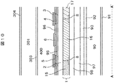
図2は、実施形態1における能動素子基板200の平面図である。図3は、実施形態1における液晶表示装置100の断面図である。図4は、実施形態1における液晶表示装置100の断面図である。図3及び図4は、夫々、図2におけるAA‘線及びBB’線に沿った断面図である。   FIG. 2 is a plan view of the active element substrate 200 according to the first embodiment. FIG. 3 is a cross-sectional view of the liquid crystal display device 100 according to the first embodiment. FIG. 4 is a cross-sectional view of the liquid crystal display device 100 according to the first embodiment. 3 and 4 are sectional views taken along lines AA 'and BB' in FIG. 2, respectively.

液晶表示装置100は、能動素子基板200、能動素子基板200の上方で対向する対向基板300、並びに能動素子基板200及び対向基板300の間に設けられた液晶層400を備える。各実施形態において、対向基板300から能動素子基板200に向かう方向を下方、能動素子基板200から対向基板300に向かう方向を上方とする。なお、図3において、バックライト装置900は、能動素子基板200の下方に設けられている。   The liquid crystal display device 100 includes an active element substrate 200, a counter substrate 300 facing above the active element substrate 200, and a liquid crystal layer 400 provided between the active element substrate 200 and the counter substrate 300. In each embodiment, a direction from the counter substrate 300 toward the active element substrate 200 is defined as a downward direction, and a direction from the active element substrate 200 toward the counter substrate 300 is defined as an upper direction. In FIG. 3, the backlight device 900 is provided below the active element substrate 200.

能動素子基板200は、カラーフィルタ1と、第2絶縁層2と、第1絶縁層3と、共通配線4と、反射抑制膜5と、絶縁層97と、絶縁層98と、画素電極6と、中継電極7と、信号線である映像信号線8と、信号線である走査信号線9と、透明基板90と、第2偏光板91と、アンダーコート膜92と、アンダーコート膜93と、半導体層94と、共通電極95と、第1配向膜96と、を備える。また、カラーフィルタ1には、第1孔である孔が形成されている。第2絶縁層2には、第2孔である孔が形成されている。   The active element substrate 200 includes the color filter 1, the second insulating layer 2, the first insulating layer 3, the common wiring 4, the reflection suppressing film 5, the insulating layer 97, the insulating layer 98, and the pixel electrode 6. The relay electrode 7, the video signal line 8 which is a signal line, the scanning signal line 9 which is a signal line, a transparent substrate 90, a second polarizing plate 91, an undercoat film 92, an undercoat film 93, A semiconductor layer 94, a common electrode 95, and a first alignment film 96 are provided. Further, the color filter 1 is formed with a hole which is a first hole. The second insulating layer 2 is formed with a second hole.

透明基板90は平板である。透明基板90はガラス製であるが、例えばプラスチック等であってもよい。第2偏光板91は、透明基板90の下に設けられている。 The transparent substrate 90 is a flat plate. The transparent substrate 90 is made of glass, but may be plastic, for example. The second polarizing plate 91 is provided under the transparent substrate 90.

アンダーコート膜92は、透明基板90上に設けられている。アンダーコート膜92は、例えば窒化ケイ素等の絶縁体物質製である。 The undercoat film 92 is provided on the transparent substrate 90. The undercoat film 92 is made of an insulating material such as silicon nitride.

アンダーコート膜93は、アンダーコート膜92上に設けられている。アンダーコート膜93は、例えば酸化ケイ素等の絶縁体物質製である。アンダーコート膜92及びアンダーコート膜93は、透明基板90からナトリウムイオン等のアルカリ成分が溶出することを防ぐ。   The undercoat film 93 is provided on the undercoat film 92. The undercoat film 93 is made of an insulating material such as silicon oxide. The undercoat film 92 and the undercoat film 93 prevent elution of alkaline components such as sodium ions from the transparent substrate 90.

半導体層94は、平面視において曲折した帯状をなしている。半導体層94は、アンダーコート膜93上の一部に設けられている。半導体層94は、ポリシリコン製である。また、半導体層94は、例えば、アモルファスシリコン製であってもよく、インジウム、ガリウム又は亜鉛等を含む酸化物半導体製であってもよい。   The semiconductor layer 94 has a bent belt shape in plan view. The semiconductor layer 94 is provided on part of the undercoat film 93. The semiconductor layer 94 is made of polysilicon. The semiconductor layer 94 may be made of, for example, amorphous silicon or an oxide semiconductor containing indium, gallium, zinc, or the like.

絶縁層97は、平板状をなしている。絶縁層97は、半導体層94が設けられていないアンダーコート膜93上、及び半導体層94上に亘って設けられている。絶縁層97は、例えば窒化シリコン製である。また、絶縁層97には、孔が、1副画素あたり2つ形成されている。絶縁層97に形成された孔は、半導体層94上の一部に、上下方向に貫通しており、下方に向かって先細りした形状である。   The insulating layer 97 has a flat plate shape. The insulating layer 97 is provided over the undercoat film 93 where the semiconductor layer 94 is not provided and over the semiconductor layer 94. The insulating layer 97 is made of, for example, silicon nitride. The insulating layer 97 has two holes per subpixel. The hole formed in the insulating layer 97 has a shape that penetrates a part of the semiconductor layer 94 in the vertical direction and tapers downward.

走査信号線9は平面視で帯状をなしている。走査信号線9は、絶縁層97上であり、各副画素の境界に設けられている。夫々の走査信号線9は、互いに平行である。また、走査信号線9は直線状であってもよく、一部が屈曲した形状をなしていてもよい。   The scanning signal line 9 has a band shape in plan view. The scanning signal line 9 is on the insulating layer 97 and is provided at the boundary of each subpixel. Each scanning signal line 9 is parallel to each other. Further, the scanning signal line 9 may be linear, or may be partially bent.

走査信号線9は、一部が後述する各画素の能動素子の一部であり、他部は能動素子と接続している。この場合、走査信号線9は、能動素子を構成する電極と電気的に接続している場合を含む。走査信号線9は、能動素子基板200に設けられた走査回路と接続し、走査回路から入力した走査信号を導通する。走査信号は、能動素子のオンオフを制御する。走査信号の電圧値は、後述する能動素子をオンにする場合は、後述する共通電極95の電位より高いゲートハイ電圧であり、能動素子をオフにする場合は、共通電極95の電位より低いゲートロー電圧である。走査信号線9は、例えばモリブデンタングステン合金等の金属製である。なお、走査信号線9は、チタンアルミ合金製であってもよい。 A part of the scanning signal line 9 is a part of an active element of each pixel described later, and the other part is connected to the active element. In this case, the scanning signal line 9 includes a case where the scanning signal line 9 is electrically connected to an electrode constituting the active element. The scanning signal line 9 is connected to a scanning circuit provided on the active element substrate 200, and conducts a scanning signal input from the scanning circuit. The scanning signal controls on / off of the active element. The voltage value of the scanning signal is a gate high voltage higher than the potential of the common electrode 95 described later when the active element described later is turned on, and the gate low voltage lower than the potential of the common electrode 95 when the active element is turned off. It is. The scanning signal line 9 is made of metal such as molybdenum tungsten alloy. The scanning signal line 9 may be made of a titanium aluminum alloy.

絶縁層98は、平板状をなしている。絶縁層98は、走査信号線9が設けられていない絶縁層97上、及び走査信号線9上に亘って設けられている。絶縁層98は、例えば窒化シリコン製である。   The insulating layer 98 has a flat plate shape. The insulating layer 98 is provided on the insulating layer 97 where the scanning signal line 9 is not provided and over the scanning signal line 9. The insulating layer 98 is made of, for example, silicon nitride.

また、絶縁層98には、上下方向に貫通しており、下方に向かって先細りした形状の孔が、1副画素あたり2つ形成されている。絶縁層98に形成された2つの孔は、絶縁層97に形成されている2つの孔の夫々の上側に形成されている。絶縁層98に形成された孔は、半導体層94上の一部に、上下方向に貫通しており、下方に向かって先細りした形状である。絶縁層98の2つの孔は、下端の形状が、絶縁層97に形成されている2つの孔の上端の形状と同じであってもよい。   The insulating layer 98 is formed with two holes per subpixel penetrating in the vertical direction and tapered downward. The two holes formed in the insulating layer 98 are formed above the two holes formed in the insulating layer 97. The hole formed in the insulating layer 98 penetrates a part of the semiconductor layer 94 in the vertical direction and has a shape that tapers downward. The two holes of the insulating layer 98 may have the same shape at the lower end as the shapes of the upper ends of the two holes formed in the insulating layer 97.

中継電極7は、平板部71と突出部72とを有する。平板部71は、絶縁層98上に設けられている。平板部71は、副画素の境界上に沿った走査信号線9同士の間隔、及び映像信号線8同士の間隔より小さい板状であり、例えば平面視において矩形状である。中継電極7は、例えばチタンアルミ合金等の金属製である。   The relay electrode 7 has a flat plate portion 71 and a protruding portion 72. The flat plate portion 71 is provided on the insulating layer 98. The flat plate portion 71 has a plate shape that is smaller than the interval between the scanning signal lines 9 and the interval between the video signal lines 8 along the boundary of the subpixel, and is, for example, a rectangular shape in plan view. The relay electrode 7 is made of metal such as titanium aluminum alloy.

また、突出部72は、平板部71の中央付近に、平板部71と連続して設けられている。突出部72は、例えば円錐形状又は円錐台形状であり、下方に突出している。突出部72の内部には、カラーフィルタ1が充填されており、下方に向かって先細りした形状である。突出部72は、側面が絶縁層98の孔及び絶縁層97の孔に沿って設けられており、下端が半導体層94の上面と接触する。   Further, the protruding portion 72 is provided continuously with the flat plate portion 71 in the vicinity of the center of the flat plate portion 71. The protrusion 72 has, for example, a cone shape or a truncated cone shape, and protrudes downward. The protrusion 72 is filled with the color filter 1 and has a shape that tapers downward. The protruding portion 72 has a side surface provided along a hole in the insulating layer 98 and a hole in the insulating layer 97, and a lower end in contact with the upper surface of the semiconductor layer 94.

映像信号線8は、各画素に設けられた後述する能動素子であるTFT(Thin Film Transistor)と接続しており、能動素子がオンの状態の際に映像信号を印加することによって、後述する液晶層400に電圧を印加する。映像信号線8は、能動素子基板200に設けられた映像信号回路と接続している。映像信号線8は、映像信号回路から入力した映像信号を導通する。映像信号線8はチタンアルミ合金等の金属製である。なお、映像信号線8は、モリブデンタングステン合金製であってもよい。   The video signal line 8 is connected to a TFT (Thin Film Transistor) which is an active element (described later) provided in each pixel, and a liquid crystal (described later) is applied by applying a video signal when the active element is on. A voltage is applied to the layer 400. The video signal line 8 is connected to a video signal circuit provided on the active element substrate 200. The video signal line 8 conducts the video signal input from the video signal circuit. The video signal line 8 is made of metal such as titanium aluminum alloy. The video signal line 8 may be made of molybdenum tungsten alloy.

映像信号線8は、線状部81と突出部82とを有し、平面視で線状をなす。線状部81は、絶縁層98上に設けられている。線状部81は、平面視において、走査信号線9に垂直な方向に沿って設けられている。線状部81は、直線部分と平面視において走査信号線9と交差する箇所において屈折している屈折部とを有する略直線状である。走査信号線9に沿った方向に隣り合う屈折部は、夫々同じ方向に屈折している。一方、走査信号線9に垂直な方向に隣り合う屈折部は、互いに逆の方向に屈折している。なお、走査信号線9は映像信号線8に垂直な直線状であってもよい。 The video signal line 8 has a linear portion 81 and a protruding portion 82, and is linear in a plan view. The linear portion 81 is provided on the insulating layer 98. The linear portion 81 is provided along a direction perpendicular to the scanning signal line 9 in plan view. The linear portion 81 is substantially linear having a straight portion and a refracting portion that is refracted at a location intersecting the scanning signal line 9 in plan view. The refracting parts adjacent in the direction along the scanning signal line 9 are refracted in the same direction. On the other hand, the refracting portions adjacent in the direction perpendicular to the scanning signal line 9 are refracted in directions opposite to each other. The scanning signal line 9 may be a straight line perpendicular to the video signal line 8.

また、突出部82は、線状部81における、中継電極7の近傍に設けられている。突出部82は、例えば円錐形状又は円錐台形状であり、下方に突出している。突出部82の内部は、カラーフィルタ1が充填されており、下方に向かって先細りした形状である。突出部82は、側面が絶縁層98の孔及び絶縁層97の孔に沿って設けられており、下端が半導体層94の上面と接触する。   Further, the protruding portion 82 is provided in the vicinity of the relay electrode 7 in the linear portion 81. The protrusion 82 has, for example, a conical shape or a truncated cone shape, and protrudes downward. The inside of the protrusion 82 is filled with the color filter 1 and has a shape that tapers downward. The projecting portion 82 has a side surface provided along a hole in the insulating layer 98 and a hole in the insulating layer 97, and a lower end in contact with the upper surface of the semiconductor layer 94.

このように、中継電極7の平板部71と、映像信号線8の線状部81とは同じ層に設けられており、中継電極7の突出部72と映像信号線8の突出部82とは、同じ半導体層94と接触している。   Thus, the flat plate portion 71 of the relay electrode 7 and the linear portion 81 of the video signal line 8 are provided in the same layer, and the protruding portion 72 of the relay electrode 7 and the protruding portion 82 of the video signal line 8 are provided. In contact with the same semiconductor layer 94.

図5は、実施形態1における能動素子基板200の平面図である。図5は、カラーフィルタ1を模式的に示している。   FIG. 5 is a plan view of the active element substrate 200 according to the first embodiment. FIG. 5 schematically shows the color filter 1.

カラーフィルタ1は、中継電極7上と、映像信号線8上と、中継電極7又は映像信号線8が設けられていない絶縁層98上とに亘って設けられている。カラーフィルタ1は、顔料粒子を含んだネガ型の有機フォトレジストである絶縁体製である。カラーフィルタ1の厚さは、例えば1〜3[μm]である。   The color filter 1 is provided over the relay electrode 7, the video signal line 8, and the insulating layer 98 where the relay electrode 7 or the video signal line 8 is not provided. The color filter 1 is made of an insulator, which is a negative organic photoresist containing pigment particles. The thickness of the color filter 1 is, for example, 1 to 3 [μm].

カラーフィルタ1は、赤のカラーフィルタ15、緑のカラーフィルタ16及び青のカラーフィルタ17を備える。赤のカラーフィルタ15、緑のカラーフィルタ16及び青のカラーフィルタ17のいずれか1つが、副画素ごとに設けられており、各色が走査信号線9に沿った方向に、周期的に繰り返されるよう並置されている。   The color filter 1 includes a red color filter 15, a green color filter 16, and a blue color filter 17. Any one of the red color filter 15, the green color filter 16, and the blue color filter 17 is provided for each sub-pixel so that each color is periodically repeated in the direction along the scanning signal line 9. It is juxtaposed.

1画素は、赤のカラーフィルタ15、緑のカラーフィルタ16及び青のカラーフィルタ17を夫々1つ備える副画素を含んでいる。また、画素は、映像信号線8及び走査信号線9に沿った方向に夫々並置されている。なお、映像信号線8は、赤のカラーフィルタ15、緑のカラーフィルタ16及び青のカラーフィルタ17夫々の境界に沿って設けられている。 One pixel includes sub-pixels each including one red color filter 15, green color filter 16, and blue color filter 17. The pixels are juxtaposed in the direction along the video signal line 8 and the scanning signal line 9. The video signal line 8 is provided along the boundaries of the red color filter 15, the green color filter 16, and the blue color filter 17.

赤のカラーフィルタ15、緑のカラーフィルタ16及び青のカラーフィルタ17夫々は、例えば同一の大きさの矩形状であるが、大きさ及び形状はそれに限られるものではない。なお、カラーフィルタ1は、他の色のフィルタであってもよい。また、カラーフィルタ1は、突出部72及び突出部82の内部にも設けられている。   Each of the red color filter 15, the green color filter 16, and the blue color filter 17 is, for example, a rectangular shape having the same size, but the size and shape are not limited thereto. The color filter 1 may be a filter of another color. The color filter 1 is also provided inside the protrusion 72 and the protrusion 82.

さらに、カラーフィルタ1には、孔が形成されている。カラーフィルタ1の孔は平板部71の上方に形成される。カラーフィルタ1の孔は、上下方向に貫通しており、下方に向かって先細りした形状である。カラーフィルタ1の孔は、例えば、上端は直径が約4[μm]の円形、下端は直径が約2[μm]の円形である。   Furthermore, holes are formed in the color filter 1. The hole of the color filter 1 is formed above the flat plate portion 71. The hole of the color filter 1 has a shape that penetrates in the vertical direction and tapers downward. The hole of the color filter 1 has, for example, a circular shape with a diameter of about 4 [μm] at the upper end and a circular shape with a diameter of about 2 [μm] at the lower end.

第2絶縁層2は、カラーフィルタ1上に設けられている。第2絶縁層2は、例えばポジ型の有機フォトレジスト製である。第2絶縁層2の厚さは、例えば1〜2[μm]である。第2絶縁層2には、カラーフィルタ1の孔の上側に、孔が形成されている。第2絶縁層2の孔は、上下方向に貫通しており、下方に向かって先細りした形状をなしている。第2絶縁層2の孔は、例えば、上端は直径が約8[μm]の円形、下端は直径が約6[μm]の円形である。   The second insulating layer 2 is provided on the color filter 1. The second insulating layer 2 is made of, for example, a positive organic photoresist. The thickness of the second insulating layer 2 is, for example, 1 to 2 [μm]. A hole is formed in the second insulating layer 2 above the hole of the color filter 1. The hole of the second insulating layer 2 penetrates in the vertical direction and has a shape that tapers downward. The hole of the second insulating layer 2 is, for example, a circle having a diameter of about 8 [μm] at the upper end and a circle having a diameter of about 6 [μm] at the lower end.

共通電極95は、第2絶縁層2上に設けられている。共通電極95は、各副画素のほぼ全域に亘る板状をなしている。また、共通電極95は、後述する画素電極6と同方向又は略同方向に伸びた帯状をなしていてもよい。共通電極95は、例えばITO(Indium Tin Oxide)、IZO(Indium Zinc Oxide)、IGO(indium gallium oxide)等酸化インジウム物質等の、透明な導電性物質製である。共通電極95は、例えば走査回路と配線を介して接続されている。共通電極95は、電圧値が一定に保たれていてもよいが、フリッカの低減等のため、走査周期と共に電圧値が変動してもよい。   The common electrode 95 is provided on the second insulating layer 2. The common electrode 95 has a plate shape over almost the entire area of each sub-pixel. Further, the common electrode 95 may have a strip shape extending in the same direction or substantially the same direction as the pixel electrode 6 described later. The common electrode 95 is made of a transparent conductive material such as an indium oxide material such as ITO (Indium Tin Oxide), IZO (Indium Zinc Oxide), or IGO (indium gallium oxide). The common electrode 95 is connected to, for example, a scanning circuit via a wiring. The voltage value of the common electrode 95 may be kept constant, but the voltage value may fluctuate with the scanning period in order to reduce flicker or the like.

共通電極95には、孔が形成されている。共通電極95の孔は第2絶縁層2に形成された孔の上端より大きい。共通電極95の孔の周縁と、第2絶縁層2の孔の周縁とが、段差を形成している。   A hole is formed in the common electrode 95. The hole of the common electrode 95 is larger than the upper end of the hole formed in the second insulating layer 2. The peripheral edge of the hole of the common electrode 95 and the peripheral edge of the hole of the second insulating layer 2 form a step.

図6は、実施形態1における能動素子基板200の平面図である。図6は、共通配線4を模式的に示している。   FIG. 6 is a plan view of the active element substrate 200 according to the first embodiment. FIG. 6 schematically shows the common wiring 4.

共通配線4は、共通電極95上に設けられている。共通配線4は、共通電極95と電気的に接続されており、望ましくは、共通電極95の直上に設けられている。共通配線4は、例えばクロムモリブデン合金製である。他にも、共通配線4は、共通電極95より低抵抗の材料製であればよく、アルミシリコン合金製であってもよい。   The common wiring 4 is provided on the common electrode 95. The common wiring 4 is electrically connected to the common electrode 95, and is preferably provided immediately above the common electrode 95. The common wiring 4 is made of, for example, a chromium molybdenum alloy. In addition, the common wiring 4 may be made of a material having a resistance lower than that of the common electrode 95, and may be made of an aluminum silicon alloy.

共通配線4は、映像信号線8及び走査信号線9に沿って設けられている。映像信号線8に沿った共通配線4は、映像信号線8より幅が広く、平面視において、映像信号線8の全部に重なっていることが望ましい。   The common wiring 4 is provided along the video signal line 8 and the scanning signal line 9. The common wiring 4 along the video signal line 8 is preferably wider than the video signal line 8 and overlaps the entire video signal line 8 in plan view.

走査信号線9に沿って設けられている共通配線4は、走査信号線9より幅が広く、平面視において、走査信号線9の全部に重なっていることが望ましい。また、共通配線4の幅が、第2絶縁層2の孔の直径よりも広い。共通配線4は、第2絶縁層2の孔と同心円上であり、第2絶縁層2の孔の上端より大きい孔が設けられている。 The common wiring 4 provided along the scanning signal line 9 is preferably wider than the scanning signal line 9 and overlaps the entire scanning signal line 9 in plan view. Further, the width of the common wiring 4 is wider than the diameter of the hole of the second insulating layer 2. The common wiring 4 is concentric with the hole of the second insulating layer 2 and has a hole larger than the upper end of the hole of the second insulating layer 2.

共通電極95がITO製である場合、金属製の場合と比較して高抵抗である。特に共通電極95の電圧値が変動している場合、電圧値の変動に遅延が発生する場合がある。共通配線4は、共通電極95より抵抗値が低いので、信号を即時に伝達することができ、電圧値の遅延を抑制することができる。 When the common electrode 95 is made of ITO, the resistance is higher than that of a metal. In particular, when the voltage value of the common electrode 95 varies, there may be a delay in the variation of the voltage value. Since the common wiring 4 has a resistance value lower than that of the common electrode 95, the signal can be transmitted immediately and the delay of the voltage value can be suppressed.

図7は、実施形態1における能動素子基板200の平面図である。図7は、反射抑制膜5を模式的に示している。   FIG. 7 is a plan view of the active element substrate 200 in the first embodiment. FIG. 7 schematically shows the reflection suppressing film 5.

反射抑制膜5は、共通配線4上に設けられている。反射抑制膜5は、平面視において共通配線4と同じ形状である。反射抑制膜5は、平面視において共通配線4より幅が広くてもよい。 The reflection suppressing film 5 is provided on the common wiring 4. The reflection suppression film 5 has the same shape as the common wiring 4 in plan view. The reflection suppression film 5 may be wider than the common wiring 4 in plan view.

反射抑制膜5は、例えば、黒色粒子を含有した非感光性の有機高分子膜製である。反射抑制膜5は、厚さが0.5[μm]である。また、反射抑制膜5は、コントラスト比の低下を抑えること、及び厚さを抑えることを両立させるため、OD(Optical Density)値が0.5〜1.0であることが望ましい。 The antireflection film 5 is made of, for example, a non-photosensitive organic polymer film containing black particles. The antireflection film 5 has a thickness of 0.5 [μm]. Further, the antireflection film 5 desirably has an OD (Optical Density) value of 0.5 to 1.0 in order to achieve both reduction in contrast ratio and suppression in thickness.

他にも、反射抑制膜5は、例えば窒化チタン製であってもよい。この場合、反射抑制膜5の厚さは、120〜140[nm]である。 In addition, the reflection suppressing film 5 may be made of, for example, titanium nitride. In this case, the thickness of the reflection suppressing film 5 is 120 to 140 [nm].

他にも、反射抑制膜5は、干渉効果を利用した多層膜であってもよい。この場合反射抑制膜5は、例えば、共通配線4に近接する側から第一の低屈折率層、高屈折率層、第二の低屈折率層を積層した構成である。この場合、例えば第一の低屈折率層と第二の低屈折率層とはITO、IZO、IGO等の酸化インジウム物質製であり、高屈折率層は、モリブデンニオブ合金製である。 In addition, the reflection suppressing film 5 may be a multilayer film using an interference effect. In this case, for example, the reflection suppressing film 5 has a configuration in which a first low refractive index layer, a high refractive index layer, and a second low refractive index layer are stacked from the side close to the common wiring 4. In this case, for example, the first low refractive index layer and the second low refractive index layer are made of an indium oxide material such as ITO, IZO, or IGO, and the high refractive index layer is made of a molybdenum niobium alloy.

上側から能動素子基板200に入射した外光は反射抑制膜5を通過して共通配線4で反射された後、再び反射抑制膜5を通過する。このように光は反射抑制膜5を二回通過するので、反射抑制膜5の透過率をT、共通配線4をRとすると、共通配線4と反射抑制膜5との積層体の反射率はTRになる。例えば反射抑制膜5の透過率を10[%]、共通配線4の反射率を20[%]とした場合、反射抑制膜5と共通配線4の積層体の反射率は0.2[%]になる。このように、本実施形態の液晶表示装置100は、外光の反射を抑え、コントラスト比の低下を抑えることができる。 External light incident on the active element substrate 200 from above passes through the reflection suppression film 5 and is reflected by the common wiring 4, and then passes through the reflection suppression film 5 again. Since light passes through the reflection suppression film 5 twice in this way, when the transmittance of the reflection suppression film 5 is T and the common wiring 4 is R, the reflectance of the laminate of the common wiring 4 and the reflection suppression film 5 is Become T 2 R. For example, when the transmittance of the reflection suppression film 5 is 10 [%] and the reflectance of the common wiring 4 is 20 [%], the reflectance of the laminated body of the reflection suppression film 5 and the common wiring 4 is 0.2 [%]. become. Thus, the liquid crystal display device 100 of this embodiment can suppress reflection of external light and suppress a decrease in contrast ratio.

第1絶縁層3は、厚さが120〜200[nm]の窒化ケイ素膜等の無機絶縁体製である。第1絶縁層3は、平板部31と突出部32とを有する。平板部31は、反射抑制膜5上、及び上方に反射抑制膜5が設けられていない共通電極95上に設けられている。突出部32は、共通電極95における孔の側面、第2絶縁層2の孔の周縁における上面及び側面、並びにカラーフィルタ1の孔の周縁における上面に沿って設けられている。よって突出部32は、下端がカラーフィルタ1上に設けられている。突出部32は、略円錐台形をなしている。   The first insulating layer 3 is made of an inorganic insulator such as a silicon nitride film having a thickness of 120 to 200 [nm]. The first insulating layer 3 has a flat plate portion 31 and a protruding portion 32. The flat plate portion 31 is provided on the antireflection film 5 and on the common electrode 95 on which the antireflection film 5 is not provided. The protrusions 32 are provided along the side surface of the hole in the common electrode 95, the upper surface and the side surface of the peripheral edge of the hole of the second insulating layer 2, and the upper surface of the peripheral edge of the hole of the color filter 1. Therefore, the lower end of the protrusion 32 is provided on the color filter 1. The protrusion 32 has a substantially truncated cone shape.

反射抑制膜5がクロムモリブデン合金製である場合、荷電性の不純物を含有する場合がある。この場合、荷電性の不純物は、液晶層400中に移動することにより、近傍の液晶層400の抵抗を低下してフリッカや残像等の不具合を生じることがある。しかし、反射抑制膜5と液晶層400との間に第1絶縁層3が設けられることにより、不純物の移動を防ぐことができる。 When the reflection suppression film 5 is made of a chromium molybdenum alloy, it may contain a chargeable impurity. In this case, the charged impurities may move into the liquid crystal layer 400, thereby reducing the resistance of the nearby liquid crystal layer 400 and causing defects such as flicker and afterimage. However, by providing the first insulating layer 3 between the antireflection film 5 and the liquid crystal layer 400, the migration of impurities can be prevented.

画素電極6は、副画素ごとに設けられており、帯状部61と突出部62とを有する。帯状部61は、各映像信号線8に沿っており、走査信号線9同士の間隔よりやや短い帯状である。画素電極6は、例えば、ITO等の透明な導電性物質製であり、厚さが50[nm]である。画素電極6の形状は、これに限らず、帯状の電極が、間隔を置いて副画素ごとに複数本並置していてもよい。   The pixel electrode 6 is provided for each sub-pixel, and has a strip-like portion 61 and a protruding portion 62. The strip portion 61 extends along each video signal line 8 and has a strip shape slightly shorter than the interval between the scanning signal lines 9. The pixel electrode 6 is made of a transparent conductive material such as ITO and has a thickness of 50 [nm]. The shape of the pixel electrode 6 is not limited to this, and a plurality of strip-shaped electrodes may be juxtaposed for each sub-pixel at an interval.

画素電極6と共通電極95とは、両者の間でフリンジ電界を生じさせる。フリンジ電界は、液晶層400の配向を制御する。また、画素電極6、第1絶縁層3及び共通電極95が重畳する部分は、コンデンサとして機能するため、電圧が印加されていない時間には、電荷を保持する。   The pixel electrode 6 and the common electrode 95 generate a fringe electric field between them. The fringe electric field controls the alignment of the liquid crystal layer 400. In addition, the portion where the pixel electrode 6, the first insulating layer 3, and the common electrode 95 overlap functions as a capacitor, and thus retains charge during a time when no voltage is applied.

突出部62は、帯状部61に連続して設けられている。突出部62は、突出部32の内側の側面及びカラーフィルタ1の孔の周縁に沿っており、段差を形成している。即ち第1絶縁層3の突出部32は、前記突出部62の側面を外側から覆っている。   The protruding portion 62 is provided continuously with the belt-like portion 61. The protrusion 62 is along the inner side surface of the protrusion 32 and the periphery of the hole of the color filter 1 and forms a step. That is, the protrusion 32 of the first insulating layer 3 covers the side surface of the protrusion 62 from the outside.

さらに、突出部62は、第1絶縁層3の突出部32より下方に突出しており、下端が中継電極7の上面と接触している。これにより、画素電極6と中継電極7とが電気的に接続する。なお、突出部62と中継電極7との間に導体の物質が設けられ、突出部62と中継電極7とが電気的に接続されていてもよい。 Further, the protruding portion 62 protrudes below the protruding portion 32 of the first insulating layer 3, and the lower end is in contact with the upper surface of the relay electrode 7. Thereby, the pixel electrode 6 and the relay electrode 7 are electrically connected. A conductor substance may be provided between the protrusion 62 and the relay electrode 7, and the protrusion 62 and the relay electrode 7 may be electrically connected.

絶縁層97と、中継電極7と、半導体層94と、それらの近傍に設けられている部分の映像信号線8及び走査信号線9とが能動素子として機能する。能動素子は、走査信号線9に印加された電圧によってオンオフを制御する。なお、中継電極7、映像信号線8又は走査信号線9に代えて、中継電極7、映像信号線8又は走査信号線9と電気的に接続した電極が能動素子として機能してもよい。能動素子は、オン時に、映像信号線8が入力した映像信号に応じた電位を、半導体層94を介して中継電極7及び画素電極6に導通する。画素電極6は、液晶層400に映像信号に応じた電位を印加する。   The insulating layer 97, the relay electrode 7, the semiconductor layer 94, and the video signal line 8 and the scanning signal line 9 in the vicinity thereof function as active elements. The active element controls on / off by the voltage applied to the scanning signal line 9. Instead of the relay electrode 7, the video signal line 8 or the scanning signal line 9, an electrode electrically connected to the relay electrode 7, the video signal line 8 or the scanning signal line 9 may function as an active element. When the active element is turned on, the active element conducts a potential corresponding to the video signal input from the video signal line 8 to the relay electrode 7 and the pixel electrode 6 through the semiconductor layer 94. The pixel electrode 6 applies a potential corresponding to the video signal to the liquid crystal layer 400.

第1配向膜96は、例えばポリイミド製であり、液晶層400の液晶分子群を一定方向に配列させる。第1配向膜96は、画素電極6が設けられていない第1絶縁層3上、及び画素電極6上に設けられている。   The first alignment film 96 is made of polyimide, for example, and arranges the liquid crystal molecule groups of the liquid crystal layer 400 in a certain direction. The first alignment film 96 is provided on the first insulating layer 3 where the pixel electrode 6 is not provided and on the pixel electrode 6.

カラーフィルタ1に形成された孔には、下端が中継電極7と接触した画素電極6と、画素電極6の内側に接触した第1配向膜96とが設けられている。従って第1配向膜96は、略円錐状であり、第1配向膜96の内側には、液晶層400が充填されている。   In the hole formed in the color filter 1, a pixel electrode 6 whose lower end is in contact with the relay electrode 7 and a first alignment film 96 in contact with the inner side of the pixel electrode 6 are provided. Accordingly, the first alignment film 96 has a substantially conical shape, and the liquid crystal layer 400 is filled inside the first alignment film 96.

第2絶縁層2に形成された孔には、孔の側面から内側に向かって、第1絶縁層3の突出部31と、突出部31の内側に接触した画素電極6の突出部62と、突出部62の内側に接触した第1配向膜96とが設けられている。第1配向膜96の内側には、液晶層400が充填されている。即ち、第1絶縁層3の突出部32は、画素電極6の突出部62を覆っている。   In the hole formed in the second insulating layer 2, the protrusion 31 of the first insulating layer 3 and the protrusion 62 of the pixel electrode 6 in contact with the inside of the protrusion 31 are formed inward from the side surface of the hole. A first alignment film 96 in contact with the inside of the protrusion 62 is provided. The liquid crystal layer 400 is filled inside the first alignment film 96. That is, the protrusion 32 of the first insulating layer 3 covers the protrusion 62 of the pixel electrode 6.

液晶層400は、配向方向の誘電率がその垂直方向よりも大きい正の誘電率異方性を有し、室温を含む広い温度範囲でネマチック相を示す。液晶層400に電圧が印加されていない場合は、ホモジニアス配向である。画素電極6が液晶層400に電圧を印加することにより、液晶層400における各液晶の方位が横方向に回転する。   The liquid crystal layer 400 has a positive dielectric anisotropy whose dielectric constant in the alignment direction is larger than that in the vertical direction, and exhibits a nematic phase in a wide temperature range including room temperature. When no voltage is applied to the liquid crystal layer 400, the alignment is homogeneous. When the pixel electrode 6 applies a voltage to the liquid crystal layer 400, the orientation of each liquid crystal in the liquid crystal layer 400 rotates in the horizontal direction.

対向基板300は、透明基板301と、第2配向膜303と、第2偏光板304とを備える。   The counter substrate 300 includes a transparent substrate 301, a second alignment film 303, and a second polarizing plate 304.

透明基板301は、例えば平板である。第2配向膜303は、対向基板300の下に設けられている。第2配向膜303の上には、オーバーコート膜が設けられていてもよい。   The transparent substrate 301 is a flat plate, for example. The second alignment film 303 is provided under the counter substrate 300. An overcoat film may be provided on the second alignment film 303.

第2偏光板304は、透明基板301の上に設けられている。第2偏光板304の吸収軸と第1偏光板91の吸収軸とは平面視において直交するように設定されている。また、例えば、第1偏光板91の吸収軸は液晶層400の配向方向に平行である。   The second polarizing plate 304 is provided on the transparent substrate 301. The absorption axis of the second polarizing plate 304 and the absorption axis of the first polarizing plate 91 are set so as to be orthogonal in a plan view. For example, the absorption axis of the first polarizing plate 91 is parallel to the alignment direction of the liquid crystal layer 400.

本実施形態によれば、共通配線4上に反射抑制膜5が設けられているので、外光が映像信号線8又は走査信号線9を反射した反射光を抑制することができる。   According to the present embodiment, since the reflection suppressing film 5 is provided on the common wiring 4, it is possible to suppress the reflected light that is reflected from the video signal line 8 or the scanning signal line 9 by the external light.

また、共通配線4と反射抑制膜5とが接触していることにより、上方のみならず斜方からの光も遮光することができ、広い角度から入射する外光の反射光を抑制することができる。   Further, since the common wiring 4 and the reflection suppressing film 5 are in contact with each other, it is possible to block not only the light from the upper side but also the oblique direction, and it is possible to suppress the reflected light of the external light incident from a wide angle. it can.

<実施形態2>
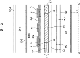
実施形態2について説明する。本実施形態は、反射抑制膜5が共通電極95の下に設けられている。
<Embodiment 2>
Embodiment 2 will be described. In the present embodiment, the reflection suppressing film 5 is provided under the common electrode 95.

図8は、実施形態2における液晶表示装置100の断面図である。図9は、実施形態2における液晶表示装置100の断面図である。図8は、図3に対応している。図9は図4に対応している。なお、以下、実施形態1と同様の構成については、説明を省略する。   FIG. 8 is a cross-sectional view of the liquid crystal display device 100 according to the second embodiment. FIG. 9 is a cross-sectional view of the liquid crystal display device 100 according to the second embodiment. FIG. 8 corresponds to FIG. FIG. 9 corresponds to FIG. Hereinafter, the description of the same configuration as that of the first embodiment will be omitted.

反射抑制膜5は実施形態1と同様の形状であり、共通電極95の直上に設けられている。   The reflection suppressing film 5 has the same shape as that of the first embodiment, and is provided immediately above the common electrode 95.

<実施形態3>
実施形態3について説明する。本実施形態は、共通電極95上に反射抑制膜5が設けられており、共通電極95の下に共通配線4が設けられている。
<Embodiment 3>
A third embodiment will be described. In this embodiment, the reflection suppression film 5 is provided on the common electrode 95, and the common wiring 4 is provided below the common electrode 95.

図10は、実施形態3における液晶表示装置100の断面図である。図11は、実施形態3における液晶表示装置100の断面図である。   FIG. 10 is a cross-sectional view of the liquid crystal display device 100 according to the third embodiment. FIG. 11 is a cross-sectional view of the liquid crystal display device 100 according to the third embodiment.

共通配線4は、共通電極95の直下に設けられており、共通電極95と電気的に接続している。一方、反射抑制膜5は、共通電極95の直上に設けられている。本実施形態の反射抑制膜5は、黒色粒子を含有した非感光性の有機高分子膜製であることが望ましい。   The common wiring 4 is provided immediately below the common electrode 95 and is electrically connected to the common electrode 95. On the other hand, the reflection suppressing film 5 is provided immediately above the common electrode 95. The antireflection film 5 of the present embodiment is desirably made of a non-photosensitive organic polymer film containing black particles.

<実施形態4>
実施形態4について説明する。本実施形態は、共通電極95と反射抑制膜5とが接触しており、かつ、共通配線4と共通電極95とが電気的に接続されている。
<Embodiment 4>
A fourth embodiment will be described. In the present embodiment, the common electrode 95 and the reflection suppressing film 5 are in contact with each other, and the common wiring 4 and the common electrode 95 are electrically connected.

図12は、実施形態4における液晶表示装置100の断面図である。図13は、実施形態4における液晶表示装置100の断面図である。本実施形態において、反射抑制膜5は、導電性の物質製である。反射抑制膜5は、共通電極95の直下に設けられており、共通電極95と電気的に接続している。   FIG. 12 is a cross-sectional view of the liquid crystal display device 100 according to the fourth embodiment. FIG. 13 is a cross-sectional view of the liquid crystal display device 100 according to the fourth embodiment. In the present embodiment, the reflection suppressing film 5 is made of a conductive substance. The antireflection film 5 is provided immediately below the common electrode 95 and is electrically connected to the common electrode 95.

共通配線4は、反射抑制膜5の下に設けられている。共通配線4は、反射抑制膜5と電気的に接続している。従って、共通電極95と、共通配線4は、電気的に接続している。この場合、例えば、共通配線4は、平面視において、実施形態1における共通配線4と同様の形状である。 The common wiring 4 is provided under the reflection suppressing film 5. The common wiring 4 is electrically connected to the reflection suppressing film 5. Therefore, the common electrode 95 and the common wiring 4 are electrically connected. In this case, for example, the common wiring 4 has the same shape as the common wiring 4 in the first embodiment in plan view.

本実施形態によれば、共通配線4が、共通電極95より下方に設けられているので、映像信号線8及び走査信号線9と近接する。これにより、共通配線4は、映像信号線8及び走査信号線9による反射光を広い範囲で抑制することができる。   According to this embodiment, since the common wiring 4 is provided below the common electrode 95, it is close to the video signal line 8 and the scanning signal line 9. Thereby, the common wiring 4 can suppress the reflected light by the video signal line 8 and the scanning signal line 9 in a wide range.

<実施形態5>
実施形態5について説明する。本実施形態は、共通配線4の幅が反射抑制膜5より狭い。
<Embodiment 5>
Embodiment 5 will be described. In the present embodiment, the width of the common wiring 4 is narrower than that of the reflection suppressing film 5.

図14は、実施形態5における液晶表示装置100の断面図である。図15は、実施形態5における液晶表示装置100の断面図である。図16は、実施形態5における能動素子基板200の平面図である。図14は、図3に対応している。図15は、図4に対応している。図16は、実施形態1における能動素子基板200の平面図である。図16は、共通配線4及び反射抑制膜5を模式的に示している。   FIG. 14 is a cross-sectional view of the liquid crystal display device 100 according to the fifth embodiment. FIG. 15 is a cross-sectional view of the liquid crystal display device 100 according to the fifth embodiment. FIG. 16 is a plan view of an active element substrate 200 according to the fifth embodiment. FIG. 14 corresponds to FIG. FIG. 15 corresponds to FIG. FIG. 16 is a plan view of the active element substrate 200 according to the first embodiment. FIG. 16 schematically shows the common wiring 4 and the reflection suppressing film 5.

走査信号線9に沿った共通配線4は、走査信号線9と同じ幅である。共通配線4は、平面視において、走査信号線9と重なる位置に設けられている。なお走査信号線9に沿った共通配線4は、走査信号線9より若干幅が広くてもよい。   The common wiring 4 along the scanning signal line 9 has the same width as the scanning signal line 9. The common wiring 4 is provided at a position overlapping the scanning signal line 9 in plan view. The common wiring 4 along the scanning signal line 9 may be slightly wider than the scanning signal line 9.

本実施形態によれば、共通配線4の幅が反射抑制膜5より狭いので、液晶表示装置100を薄型化し軽量化する一方、外光が映像信号線8又は走査信号線9を反射した反射光を抑制することができる。   According to the present embodiment, since the width of the common wiring 4 is narrower than that of the reflection suppressing film 5, the liquid crystal display device 100 is reduced in thickness and weight, while reflected light from which external light is reflected from the video signal line 8 or the scanning signal line 9. Can be suppressed.

<実施形態6>
実施形態6について説明する。本実施形態は、共通配線4と反射抑制膜5とを一括形成する。
<Embodiment 6>
Embodiment 6 will be described. In the present embodiment, the common wiring 4 and the reflection suppressing film 5 are collectively formed.

図17Aは、実施形態6における液晶表示装置100の製造方法を示す図である。図17Bは、実施形態6における液晶表示装置100の製造方法を示す図である。図17A及び図17Bは、共通電極95、共通配線4及び反射抑制膜5の製造方法を示す。 FIG. 17A is a diagram illustrating the method of manufacturing the liquid crystal display device 100 according to the sixth embodiment. FIG. 17B is a diagram illustrating the method of manufacturing the liquid crystal display device 100 according to the sixth embodiment. 17A and 17B show a method for manufacturing the common electrode 95, the common wiring 4, and the reflection suppressing film 5.

製造方法について説明する。図17A(a)に示すように、下から共通電極95、共通配線4及び反射抑制膜5が設けられている(S1)。   A manufacturing method will be described. As shown in FIG. 17A (a), the common electrode 95, the common wiring 4 and the reflection suppressing film 5 are provided from the bottom (S1).

図17A(b)に示すように、レジスト600が反射抑制膜5上に塗布される(S2)。レジスト600は、例えばインクジェット方式により塗布される。図17A(c)に示すように、レジスト600が現像される(S3)。これにより、レジスト600が所望の形状になる。   As shown in FIG. 17A (b), a resist 600 is applied on the antireflection film 5 (S2). The resist 600 is applied by, for example, an ink jet method. As shown in FIG. 17A (c), the resist 600 is developed (S3). Thereby, the resist 600 becomes a desired shape.

図17B(d)に示すように、反射抑制膜5が、レジストの形状に沿ってエッチングされる(S4)。反射抑制膜5は、例えばアルカリ性の溶液によってエッチングされる。これにより、反射抑制膜5は、平面視において、レジストとほぼ同じ形状になる。図17B(e)に示すように、共通配線4が、レジストの形状に沿ってエッチングされる(S5)。共通配線4は、例えば酸性の溶液によってエッチングされる。これにより、共通配線4は、平面視において、レジスト及び反射抑制膜5とほぼ同じ形状になる。 図17B(f)に示すように、最後にレジスト600が反射抑制膜5上から除去される(S6)。   As shown in FIG. 17B (d), the reflection suppressing film 5 is etched along the shape of the resist (S4). The antireflection film 5 is etched by, for example, an alkaline solution. Thereby, the reflection suppressing film 5 has substantially the same shape as the resist in plan view. As shown in FIG. 17B (e), the common wiring 4 is etched along the shape of the resist (S5). The common wiring 4 is etched by an acidic solution, for example. Thereby, the common wiring 4 has substantially the same shape as the resist and the reflection suppressing film 5 in a plan view. As shown in FIG. 17B (f), the resist 600 is finally removed from the reflection suppressing film 5 (S6).

本実施形態によれば、共通配線4と反射抑制膜5とが一括でエッチングされるので、共通配線4と反射抑制膜5との位置のずれを低減することができる。   According to this embodiment, since the common wiring 4 and the reflection suppressing film 5 are etched at once, the positional shift between the common wiring 4 and the reflection suppressing film 5 can be reduced.

<実施形態7>
実施形態7について説明する。本実施形態は、共通配線4が映像信号線8と反射抑制膜5との間に設けられている。
<Embodiment 7>
A seventh embodiment will be described. In the present embodiment, the common wiring 4 is provided between the video signal line 8 and the reflection suppressing film 5.

図18は、実施形態7における液晶表示装置100の断面図である。図19は、実施形態7における液晶表示装置100の断面図である。図20は、実施形態7における液能動素子基板200の平面図である。図18は、図3に対応している。図19は、図4に対応している。図20は、実施形態1における能動素子基板200の平面図である。図16は、共通配線4及び反射抑制膜5を模式的に示している。   FIG. 18 is a cross-sectional view of the liquid crystal display device 100 according to the seventh embodiment. FIG. 19 is a cross-sectional view of the liquid crystal display device 100 according to the seventh embodiment. FIG. 20 is a plan view of the liquid active element substrate 200 according to the seventh embodiment. FIG. 18 corresponds to FIG. FIG. 19 corresponds to FIG. FIG. 20 is a plan view of the active element substrate 200 according to the first embodiment. FIG. 16 schematically shows the common wiring 4 and the reflection suppressing film 5.

共通配線4は、帯状部41と突出部42とを備える。共通配線4は、映像信号線8の直上に設けられている。即ち、帯状部41は線状部81の直上に設けられ、突出部42は突出部82の直上に設けられている。また、共通配線4は、中継電極7の直上に設けられていてもよい。この場合、画素電極6の突出部62は、突出部42を介して中継電極7と物理的に接触することにより、中継電極7と電気的に接続する。   The common wiring 4 includes a belt-like portion 41 and a protruding portion 42. The common wiring 4 is provided immediately above the video signal line 8. That is, the belt-like portion 41 is provided immediately above the linear portion 81, and the protruding portion 42 is provided immediately above the protruding portion 82. Further, the common wiring 4 may be provided immediately above the relay electrode 7. In this case, the protrusion 62 of the pixel electrode 6 is electrically connected to the relay electrode 7 by physically contacting the relay electrode 7 via the protrusion 42.

また、映像信号線8及び共通配線4は、反射抑制膜5より幅が狭い。これにより、外光が映像信号線8又は走査信号線9を反射した反射光について、多様な角度から入射する外光の反射光抑制することができる。   In addition, the video signal line 8 and the common wiring 4 are narrower than the reflection suppression film 5. As a result, the reflected light of the external light incident from various angles can be suppressed for the reflected light of the external light reflected from the video signal line 8 or the scanning signal line 9.

なお、共通配線4は、映像信号線8と反射抑制膜5との間に設けられていればよく、映像信号線8の直上であることに限られない。例えば共通配線4は、第2絶縁層2上に設けられていてもよい。 The common wiring 4 only needs to be provided between the video signal line 8 and the reflection suppression film 5, and is not limited to being directly above the video signal line 8. For example, the common wiring 4 may be provided on the second insulating layer 2.

<実施形態8>
実施形態8について説明する。本実施形態は、反射抑制膜5が、画素電極6における突出部62の上方に設けられている。
<Embodiment 8>
Embodiment 8 will be described. In the present embodiment, the reflection suppressing film 5 is provided above the protrusion 62 in the pixel electrode 6.

図21は、実施形態8における液晶表示装置100の断面図である。図22は、実施形態8における液晶表示装置100の断面図である。 FIG. 21 is a cross-sectional view of the liquid crystal display device 100 according to the eighth embodiment. FIG. 22 is a cross-sectional view of the liquid crystal display device 100 according to the eighth embodiment.

共通配線4は、共通電極95上に設けられている。第1絶縁層3は、共通配線4上及び共通配線4の設けられていない共通電極95上に設けられている。   The common wiring 4 is provided on the common electrode 95. The first insulating layer 3 is provided on the common wiring 4 and on the common electrode 95 where the common wiring 4 is not provided.

反射抑制膜5は、平板部51と突出部52とを備える。平板部51は、第1絶縁層3上の平板部31上に設けられている。突出部52は、平板部51と連続しており、画素電極6の突出部62に沿って突出している。従って、突出部52は、突出部62の内側であり、上方に設けられている。   The reflection suppressing film 5 includes a flat plate portion 51 and a protruding portion 52. The flat plate portion 51 is provided on the flat plate portion 31 on the first insulating layer 3. The protruding portion 52 is continuous with the flat plate portion 51 and protrudes along the protruding portion 62 of the pixel electrode 6. Accordingly, the protruding portion 52 is provided inside and above the protruding portion 62.

本実施形態によれば、反射抑制膜5が、画素電極6における突出部62の上方に突出部52を有するので、カラーフィルタ1及び第2絶縁層2の孔内及び孔の近傍における反射光を抑制することができる。特に、反射抑制膜5は、画素電極6の突出部62、中継電極7を反射する反射光を抑制することができる。   According to the present embodiment, since the reflection suppressing film 5 has the protruding portion 52 above the protruding portion 62 in the pixel electrode 6, the reflected light in and near the holes of the color filter 1 and the second insulating layer 2 is reflected. Can be suppressed. In particular, the reflection suppression film 5 can suppress the reflected light that reflects the protrusion 62 of the pixel electrode 6 and the relay electrode 7.

なお、第2絶縁層2の突出部22は、カラーフィルタ1の孔内にまで設けられていてもよく、中継電極7に接触していてもよい。 The protruding portion 22 of the second insulating layer 2 may be provided up to the hole of the color filter 1 or may be in contact with the relay electrode 7.

なお、反射抑制膜5の突出部52は、突出部62の一部の上方にのみ設けられていてもよい。例えば、突出部52は、第2絶縁層2の孔内にのみ設けられていてもよい。 The protrusion 52 of the reflection suppressing film 5 may be provided only above a part of the protrusion 62. For example, the protrusion 52 may be provided only in the hole of the second insulating layer 2.

本実施形態によれば、反射抑制膜5と第1配向膜96との間に第3絶縁層99が設けられているので、反射抑制膜5から生じる不純物が液晶に移動することを防止する。   According to the present embodiment, since the third insulating layer 99 is provided between the reflection suppression film 5 and the first alignment film 96, the impurities generated from the reflection suppression film 5 are prevented from moving to the liquid crystal.

<実施形態9>
実施形態9について説明する。本実施形態は、第3絶縁層99が設けられている。
<Ninth Embodiment>
Embodiment 9 will be described. In the present embodiment, a third insulating layer 99 is provided.

図23は、実施形態9における液晶表示装置100の断面図である。図24は、実施形態9における液晶表示装置100の断面図である。本実施形態は、実施形態8と比較し、反射抑制膜5と第1配向膜96との間に第3絶縁層99が設けられている。 FIG. 23 is a cross-sectional view of the liquid crystal display device 100 according to the ninth embodiment. FIG. 24 is a cross-sectional view of the liquid crystal display device 100 according to the ninth embodiment. In the present embodiment, a third insulating layer 99 is provided between the reflection suppressing film 5 and the first alignment film 96 as compared with the eighth embodiment.

第3絶縁層99は、反射抑制膜5における平板部51及び突出部52上に設けられている。第3絶縁層99は、平板部51及び突出部52の一方のみに設けられていてもよい。配向膜96は、第3絶縁層99上、第3絶縁層99が上方に設けられていない画素電極6上、及び第3絶縁層99も画素電極6も設けられていない第1絶縁層3上に設けられている。   The third insulating layer 99 is provided on the flat plate portion 51 and the protruding portion 52 in the reflection suppressing film 5. The third insulating layer 99 may be provided only on one of the flat plate portion 51 and the protruding portion 52. The alignment film 96 is on the third insulating layer 99, on the pixel electrode 6 where the third insulating layer 99 is not provided above, and on the first insulating layer 3 where neither the third insulating layer 99 nor the pixel electrode 6 is provided. Is provided.

<実施形態10>
上述の実施形態における、画素電極6は、共通電極95より上に設けられていたが、共通電極95が画素電極6より上に設けられていてもよい。また、共通電極95が平面視で帯状等の形状をなしている場合は、画素電極6は、共通電極95と同じ層に設けられていてもよい。
<Embodiment 10>
In the above-described embodiment, the pixel electrode 6 is provided above the common electrode 95, but the common electrode 95 may be provided above the pixel electrode 6. In addition, when the common electrode 95 has a band shape or the like in plan view, the pixel electrode 6 may be provided in the same layer as the common electrode 95.

また、上述の実施形態におけるカラーフィルタ1に代えて、カラーフィルタ1と位置及び形状を同じくする第2絶縁層2が設けられていてもよい。この場合、第2絶縁層2に代えて、第2絶縁層2と位置及び形状を同じくするカラーフィルタ1が設けられる。   Moreover, it replaces with the color filter 1 in the above-mentioned embodiment, and the 2nd insulating layer 2 which has the same position and shape as the color filter 1 may be provided. In this case, a color filter 1 having the same position and shape as the second insulating layer 2 is provided in place of the second insulating layer 2.

今回開示された実施形態はすべての点で例示であって、制限的なものでは無いと考えられるべきである。本発明の範囲は、上記した意味では無く、特許請求の範囲によって示され、特許請求の範囲と均等の意味及び範囲内でのすべての変更が含まれることが意図される。また、各実施の形態に記載されている技術的特徴は、相互に組合せ可能であり、組み合わせることにより、新しい技術的特徴を形成することができる。 It should be thought that embodiment disclosed this time is an illustration and restrictive at no points. The scope of the present invention is defined not by the above-mentioned meaning but by the scope of the claims, and is intended to include all modifications within the meaning and scope equivalent to the scope of the claims. The technical features described in each embodiment can be combined with each other, and a new technical feature can be formed by combining them.

100 表示装置
200 能動素子基板
1 カラーフィルタ、11 板状部、 12 突出部、 15 赤カラーフィルタ、 16 緑カラーフィルタ、 17 青カラーフィルタ
2 第2絶縁層
3 第1絶縁層 31 板状部、 32 突出部
4 共通配線、 41 帯状部、 42 突出部
5 反射抑制膜、 51 板状部、 52 突出部
6 画素電極、 61 帯状部、 62 突出部
7 中継電極、 71 平板部、 72 突出部
8 映像信号線、81 線状部、 82 突出部
9 走査信号線
90 透明基板
91 第1偏光板
92 第1アンダーコート膜
93 第2アンダーコート膜
94 半導体層
95 共通電極
96 第1配向膜
97、98 絶縁層
99 第3絶縁層
300 対向基板
301 透明基板
302 オーバーコート膜
303 第2配向膜
304 第2偏光版
400 液晶層
600 レジスト
900 バックライト装置
DESCRIPTION OF SYMBOLS 100 Display apparatus 200 Active element board | substrate 1 Color filter, 11 Plate-shaped part, 12 Protrusion part, 15 Red color filter, 16 Green color filter, 17 Blue color filter 2 2nd insulating layer 3 1st insulating layer 31 Plate-shaped part, 32 Projection part 4 Common wiring, 41 Band part, 42 Projection part 5 Antireflection film, 51 Plate part, 52 Projection part 6 Pixel electrode, 61 Band part, 62 Projection part 7 Relay electrode, 71 Flat plate part, 72 Projection part 8 Video Signal line 81 Linear portion 82 Projection portion 9 Scanning signal line 90 Transparent substrate 91 First polarizing plate 92 First undercoat film 93 Second undercoat film 94 Semiconductor layer 95 Common electrode 96 First alignment films 97, 98 Insulation Layer 99 Third insulating layer 300 Counter substrate 301 Transparent substrate 302 Overcoat film 303 Second alignment film 304 Second polarizing plate 400 Liquid crystal layer 600 Resist 900 Backlight apparatus

Claims (9)

第1基板、前記第1基板上に設けられた液晶層、及び前記液晶層上に設けられた第2基板を備える液晶表示装置であって、
前記第1基板は、
カラーフィルタと、
前記カラーフィルタ上に設けられた共通電極と、
前記共通電極と電気的に接続している共通配線と、
前記共通配線上及び前記カラーフィルタ上に設けられた反射抑制膜と、
前記共通電極との間に電界を発生させる画素電極と、
前記共通電極及び前記画素電極の間に設けられた第1絶縁層と、を備える
液晶表示装置。
A liquid crystal display device comprising a first substrate, a liquid crystal layer provided on the first substrate, and a second substrate provided on the liquid crystal layer,
The first substrate is
A color filter,
A common electrode provided on the color filter;
Common wiring electrically connected to the common electrode;
A reflection suppressing film provided on the common wiring and the color filter;
A pixel electrode for generating an electric field between the common electrode;
And a first insulating layer provided between the common electrode and the pixel electrode.
前記共通配線の下に設けられており、信号を導通する金属製の信号線を備え、
前記共通配線は、前記信号線上に、平面視で前記信号線に沿って設けられている
請求項1に記載の液晶表示装置。
Provided under the common wiring, comprising a metal signal line for conducting the signal,
The liquid crystal display device according to claim 1, wherein the common wiring is provided on the signal line along the signal line in a plan view.
前記反射抑制膜は、前記共通電極上に設けられている
請求項2に記載の液晶表示装置。
The liquid crystal display device according to claim 2, wherein the antireflection film is provided on the common electrode.
前記カラーフィルタに接触した第2絶縁層を備え、
前記共通電極は、前記前記第2絶縁層上に設けられている
請求項3に記載の液晶表示装置。
A second insulating layer in contact with the color filter;
The liquid crystal display device according to claim 3, wherein the common electrode is provided on the second insulating layer.
前記信号は映像信号であり、
前記信号線に導かれた映像信号を導通する半導体層と、
前記半導体層に導かれた映像信号を導通する中継電極と、を備え、
前記カラーフィルタには、第1孔が形成されており、
前記第2絶縁層には、第2孔が形成されており、
前記画素電極は、前記共通電極、前記カラーフィルタ及び前記第2絶縁層上に設けられた平板部と、前記第1孔及び第2孔の内部に突出しており、前記中継電極と電気的に接続した第1突出部とを有する
請求項4に記載の液晶表示装置。
The signal is a video signal;
A semiconductor layer for conducting a video signal led to the signal line;
A relay electrode for conducting a video signal guided to the semiconductor layer,
A first hole is formed in the color filter,
A second hole is formed in the second insulating layer,
The pixel electrode protrudes into the flat portion provided on the common electrode, the color filter, and the second insulating layer, and the first hole and the second hole, and is electrically connected to the relay electrode. The liquid crystal display device according to claim 4, further comprising a first protruding portion.
前記反射抑制膜は、前記第1突出部上に設けられた第2突出部を有する
請求項5に記載の液晶表示装置。
The liquid crystal display device according to claim 5, wherein the antireflection film has a second protrusion provided on the first protrusion.
前記反射抑制膜は、導電性物質製であり、
前記反射抑制膜は、前記共通電極の下に設けられており、
前記共通電極及び前記共通配線は、電気的に接続している
請求項2に記載の液晶表示装置。
The antireflection film is made of a conductive material,
The antireflection film is provided under the common electrode,
The liquid crystal display device according to claim 2, wherein the common electrode and the common wiring are electrically connected.
前記共通配線は、前記共通電極の下に設けられている
請求項2から4までのいずれか1項に記載の液晶表示装置。
5. The liquid crystal display device according to claim 2, wherein the common wiring is provided under the common electrode. 6.
前記反射抑制膜上に設けられた第3絶縁層を備える
請求項1から8までのいずれか1項に記載の液晶表示装置。
The liquid crystal display device according to claim 1, further comprising a third insulating layer provided on the reflection suppression film.
JP2014253260A 2014-12-15 2014-12-15 Liquid crystal display device Pending JP2016114779A (en)

Priority Applications (3)

Application Number Priority Date Filing Date Title
JP2014253260A JP2016114779A (en) 2014-12-15 2014-12-15 Liquid crystal display device
CN201521005674.7U CN205353531U (en) 2014-12-15 2015-12-07 Liquid crystal display device
US14/967,868 US9690131B2 (en) 2014-12-15 2015-12-14 Liquid crystal display device

Applications Claiming Priority (1)

Application Number Priority Date Filing Date Title
JP2014253260A JP2016114779A (en) 2014-12-15 2014-12-15 Liquid crystal display device

Publications (1)

Publication Number Publication Date
JP2016114779A true JP2016114779A (en) 2016-06-23

Family

ID=56111030

Family Applications (1)

Application Number Title Priority Date Filing Date
JP2014253260A Pending JP2016114779A (en) 2014-12-15 2014-12-15 Liquid crystal display device

Country Status (3)

Country Link
US (1) US9690131B2 (en)
JP (1) JP2016114779A (en)
CN (1) CN205353531U (en)

Cited By (2)

* Cited by examiner, † Cited by third party
Publication number Priority date Publication date Assignee Title
JP2018031977A (en) * 2016-08-26 2018-03-01 株式会社ジャパンディスプレイ Display device
JP2024021515A (en) * 2022-08-03 2024-02-16 株式会社ジャパンディスプレイ Display device and display system

Families Citing this family (3)

* Cited by examiner, † Cited by third party
Publication number Priority date Publication date Assignee Title
CN110767660B (en) * 2018-07-24 2022-09-16 京东方科技集团股份有限公司 Array substrate, preparation method thereof and display panel
CN111443532A (en) * 2020-04-21 2020-07-24 Tcl华星光电技术有限公司 Liquid crystal display panel and display device
TWI747707B (en) * 2020-08-03 2021-11-21 友達光電股份有限公司 Pixel array substrate

Family Cites Families (2)

* Cited by examiner, † Cited by third party
Publication number Priority date Publication date Assignee Title
JP2002350886A (en) 2001-05-28 2002-12-04 Matsushita Electric Ind Co Ltd Manufacturing method of liquid crystal display device and liquid crystal display device
US9201276B2 (en) * 2012-10-17 2015-12-01 Apple Inc. Process architecture for color filter array in active matrix liquid crystal display

Cited By (2)

* Cited by examiner, † Cited by third party
Publication number Priority date Publication date Assignee Title
JP2018031977A (en) * 2016-08-26 2018-03-01 株式会社ジャパンディスプレイ Display device
JP2024021515A (en) * 2022-08-03 2024-02-16 株式会社ジャパンディスプレイ Display device and display system

Also Published As

Publication number Publication date
US20160170259A1 (en) 2016-06-16
CN205353531U (en) 2016-06-29
US9690131B2 (en) 2017-06-27

Similar Documents

Publication Publication Date Title
US8098357B2 (en) Liquid crystal display panel
US10288955B2 (en) Liquid crystal display device
CN104423107B (en) Liquid crystal disply device and its preparation method
US20140267962A1 (en) Liquid crystal display
JP6599608B2 (en) Liquid crystal display
US9086604B2 (en) Arrray substrate and display device
JP2009186869A (en) Liquid crystal display device
US9766512B2 (en) Liquid crystal display panel
US9551905B2 (en) Display device
US10295871B2 (en) Liquid crystal display panel and liquid crystal display device
JP2017044915A (en) Liquid crystal display device
JP2013182127A (en) Liquid crystal display
CN205353531U (en) Liquid crystal display device
US10768496B2 (en) Thin film transistor substrate and display panel
US10620487B2 (en) Pixel structure, array substrate, display device and method for manufacturing the same
TWI553877B (en) Thin film transistor substrate, display panel and display device
JP2020109505A (en) Liquid crystal display device
JP2017097053A (en) Liquid crystal display device
US10606139B2 (en) Pixel structure
JP2015197628A (en) liquid crystal display device
US10895791B2 (en) Active matrix substrate and liquid crystal display device
JP2013134317A (en) Liquid crystal display device
US8384869B2 (en) Liquid crystal display device
JP2016038539A (en) Liquid crystal display device
JP2011154101A (en) Liquid crystal display panel and liquid crystal display device