JP2010020241A - Display apparatus, method of driving display apparatus, drive-use integrated circuit, driving method employed by drive-use integrated circuit, and signal processing method - Google Patents
Display apparatus, method of driving display apparatus, drive-use integrated circuit, driving method employed by drive-use integrated circuit, and signal processing method Download PDFInfo
- Publication number
- JP2010020241A JP2010020241A JP2008183033A JP2008183033A JP2010020241A JP 2010020241 A JP2010020241 A JP 2010020241A JP 2008183033 A JP2008183033 A JP 2008183033A JP 2008183033 A JP2008183033 A JP 2008183033A JP 2010020241 A JP2010020241 A JP 2010020241A
- Authority
- JP
- Japan
- Prior art keywords
- signal
- input image
- brightness
- image signal
- modulation level
- Prior art date
- Legal status (The legal status is an assumption and is not a legal conclusion. Google has not performed a legal analysis and makes no representation as to the accuracy of the status listed.)
- Pending
Links
Images


Classifications
-
- G—PHYSICS
- G09—EDUCATION; CRYPTOGRAPHY; DISPLAY; ADVERTISING; SEALS
- G09G—ARRANGEMENTS OR CIRCUITS FOR CONTROL OF INDICATING DEVICES USING STATIC MEANS TO PRESENT VARIABLE INFORMATION
- G09G3/00—Control arrangements or circuits, of interest only in connection with visual indicators other than cathode-ray tubes
- G09G3/20—Control arrangements or circuits, of interest only in connection with visual indicators other than cathode-ray tubes for presentation of an assembly of a number of characters, e.g. a page, by composing the assembly by combination of individual elements arranged in a matrix no fixed position being assigned to or needed to be assigned to the individual characters or partial characters
- G09G3/34—Control arrangements or circuits, of interest only in connection with visual indicators other than cathode-ray tubes for presentation of an assembly of a number of characters, e.g. a page, by composing the assembly by combination of individual elements arranged in a matrix no fixed position being assigned to or needed to be assigned to the individual characters or partial characters by control of light from an independent source
- G09G3/36—Control arrangements or circuits, of interest only in connection with visual indicators other than cathode-ray tubes for presentation of an assembly of a number of characters, e.g. a page, by composing the assembly by combination of individual elements arranged in a matrix no fixed position being assigned to or needed to be assigned to the individual characters or partial characters by control of light from an independent source using liquid crystals
-
- G—PHYSICS
- G09—EDUCATION; CRYPTOGRAPHY; DISPLAY; ADVERTISING; SEALS
- G09G—ARRANGEMENTS OR CIRCUITS FOR CONTROL OF INDICATING DEVICES USING STATIC MEANS TO PRESENT VARIABLE INFORMATION
- G09G3/00—Control arrangements or circuits, of interest only in connection with visual indicators other than cathode-ray tubes
- G09G3/20—Control arrangements or circuits, of interest only in connection with visual indicators other than cathode-ray tubes for presentation of an assembly of a number of characters, e.g. a page, by composing the assembly by combination of individual elements arranged in a matrix no fixed position being assigned to or needed to be assigned to the individual characters or partial characters
- G09G3/34—Control arrangements or circuits, of interest only in connection with visual indicators other than cathode-ray tubes for presentation of an assembly of a number of characters, e.g. a page, by composing the assembly by combination of individual elements arranged in a matrix no fixed position being assigned to or needed to be assigned to the individual characters or partial characters by control of light from an independent source
- G09G3/3406—Control of illumination source
- G09G3/3413—Details of control of colour illumination sources
-
- G—PHYSICS
- G02—OPTICS
- G02F—OPTICAL DEVICES OR ARRANGEMENTS FOR THE CONTROL OF LIGHT BY MODIFICATION OF THE OPTICAL PROPERTIES OF THE MEDIA OF THE ELEMENTS INVOLVED THEREIN; NON-LINEAR OPTICS; FREQUENCY-CHANGING OF LIGHT; OPTICAL LOGIC ELEMENTS; OPTICAL ANALOGUE/DIGITAL CONVERTERS
- G02F1/00—Devices or arrangements for the control of the intensity, colour, phase, polarisation or direction of light arriving from an independent light source, e.g. switching, gating or modulating; Non-linear optics
- G02F1/01—Devices or arrangements for the control of the intensity, colour, phase, polarisation or direction of light arriving from an independent light source, e.g. switching, gating or modulating; Non-linear optics for the control of the intensity, phase, polarisation or colour
- G02F1/13—Devices or arrangements for the control of the intensity, colour, phase, polarisation or direction of light arriving from an independent light source, e.g. switching, gating or modulating; Non-linear optics for the control of the intensity, phase, polarisation or colour based on liquid crystals, e.g. single liquid crystal display cells
- G02F1/133—Constructional arrangements; Operation of liquid crystal cells; Circuit arrangements
-
- G—PHYSICS
- G09—EDUCATION; CRYPTOGRAPHY; DISPLAY; ADVERTISING; SEALS
- G09G—ARRANGEMENTS OR CIRCUITS FOR CONTROL OF INDICATING DEVICES USING STATIC MEANS TO PRESENT VARIABLE INFORMATION
- G09G3/00—Control arrangements or circuits, of interest only in connection with visual indicators other than cathode-ray tubes
- G09G3/20—Control arrangements or circuits, of interest only in connection with visual indicators other than cathode-ray tubes for presentation of an assembly of a number of characters, e.g. a page, by composing the assembly by combination of individual elements arranged in a matrix no fixed position being assigned to or needed to be assigned to the individual characters or partial characters
- G09G3/34—Control arrangements or circuits, of interest only in connection with visual indicators other than cathode-ray tubes for presentation of an assembly of a number of characters, e.g. a page, by composing the assembly by combination of individual elements arranged in a matrix no fixed position being assigned to or needed to be assigned to the individual characters or partial characters by control of light from an independent source
- G09G3/3406—Control of illumination source
-
- G—PHYSICS
- G09—EDUCATION; CRYPTOGRAPHY; DISPLAY; ADVERTISING; SEALS
- G09G—ARRANGEMENTS OR CIRCUITS FOR CONTROL OF INDICATING DEVICES USING STATIC MEANS TO PRESENT VARIABLE INFORMATION
- G09G2340/00—Aspects of display data processing
- G09G2340/06—Colour space transformation
-
- G—PHYSICS
- G09—EDUCATION; CRYPTOGRAPHY; DISPLAY; ADVERTISING; SEALS
- G09G—ARRANGEMENTS OR CIRCUITS FOR CONTROL OF INDICATING DEVICES USING STATIC MEANS TO PRESENT VARIABLE INFORMATION
- G09G5/00—Control arrangements or circuits for visual indicators common to cathode-ray tube indicators and other visual indicators
- G09G5/02—Control arrangements or circuits for visual indicators common to cathode-ray tube indicators and other visual indicators characterised by the way in which colour is displayed
Landscapes
- Engineering & Computer Science (AREA)
- Physics & Mathematics (AREA)
- General Physics & Mathematics (AREA)
- Theoretical Computer Science (AREA)
- Computer Hardware Design (AREA)
- Crystallography & Structural Chemistry (AREA)
- Nonlinear Science (AREA)
- Chemical & Material Sciences (AREA)
- Optics & Photonics (AREA)
- Mathematical Physics (AREA)
- Control Of Indicators Other Than Cathode Ray Tubes (AREA)
- Liquid Crystal Display Device Control (AREA)
- Liquid Crystal (AREA)
Abstract
Description
本発明は、例えば表示装置等に係り、特に集積回路(IC;Integrated Circuit)のサイズの縮小、更にはコストダウン等を実現する技術分野に関する。 The present invention relates to, for example, a display device, and more particularly to a technical field that realizes reduction in the size of an integrated circuit (IC) and further cost reduction.
近年、表示装置の高機能化、多用途化に伴って、画像を適切な状態で表示できるように入力画像信号によって輝度やコントラストなどを最適な状態に調整する種々の技術が開発されている。例えば、特許文献1では、入力画像信号における白輝度の割合を検出し、検出結果を輝度調整回路にフィードバックすることにより、表示内容の変化に対して表示画面の輝度を一定に保つことを目的とした技術が開示されている。 2. Description of the Related Art In recent years, various techniques for adjusting brightness, contrast, and the like with an input image signal to an optimal state have been developed so that an image can be displayed in an appropriate state as the display device becomes more sophisticated and versatile. For example, Patent Document 1 aims to keep the luminance of a display screen constant with respect to a change in display content by detecting a white luminance ratio in an input image signal and feeding back a detection result to a luminance adjustment circuit. Have been disclosed.
その一方、赤(R;Red)、緑(G;Green)、青(B;Blue)の3色に加えてホワイト(W;White)のサブピクセルを用いた所謂RGBWディスプレイによれば、入力されたRGB画像信号をRGBW画像信号に変換することで、明るさを向上し、結果として消費電力を低減させることが可能となる。例えば、特許文献2では、入力RGB画像信号をRGBW画像信号に変換し、これをバッファ部に蓄積し、その後、表示装置に送り、表示を行なうシステムが開示されている。 On the other hand, according to a so-called RGBW display using three sub-pixels of white (W; White) in addition to three colors of red (R; Red), green (G; Green), and blue (B; Blue). By converting the RGB image signal into the RGBW image signal, the brightness can be improved, and as a result, the power consumption can be reduced. For example, Patent Document 2 discloses a system that converts an input RGB image signal into an RGBW image signal, accumulates it in a buffer unit, and then sends it to a display device for display.
しかしながら、前述した従来技術のうち、前者の場合には入力画像信号をフレームメモリに蓄える必要がある。そして、後者の場合にはRGBW変換後の画像信号をフレームメモリに蓄える必要がある。したがって、いずれの場合においてもフレームメモリ分のICのサイズアップ、コストアップが問題となっていた。 However, among the above-described conventional techniques, in the former case, it is necessary to store the input image signal in the frame memory. In the latter case, it is necessary to store the RGBW converted image signal in the frame memory. Therefore, in any case, there has been a problem of increasing the size and cost of the IC for the frame memory.
そこで、本発明では、フレームメモリを用いずに画像信号処理を行なうことで、ICサイズの縮小、更にはコストダウンを実現し、より簡易に高機能で且つ低消費電力な表示を実現することを課題とする。 Therefore, in the present invention, by performing image signal processing without using a frame memory, it is possible to reduce the IC size and further reduce the cost, and to realize a display with high functionality and low power consumption more easily. Let it be an issue.
本発明の第1の観点による表示装置は、赤、緑、青に加えて更に所定色の出力用サブピクセルが配列されピクセルを構成する表示画素部と、前記入力画像信号の信号レベルを伸張し、この伸張した赤、緑、青の信号から前記所定色の信号成分を抽出し、該所定色の信号レベルを決定し、この決定された所定色の信号レベルに基づいて伸張処理を行い、この伸張処理後の赤、緑、青の信号を所定の変調レベルに従って変調することで元の画像と異なる明るさに変調し、同時に光源の明るさを変調する信号処理部とを備え、前記変調レベルを決定するための入力画像信号と、変調処理をして前記表示画素部にて表示を行う入力画像信号が異なるフレームのものである。 A display device according to a first aspect of the present invention includes a display pixel unit in which output sub-pixels of a predetermined color are further arranged in addition to red, green, and blue, and a signal level of the input image signal. The signal component of the predetermined color is extracted from the expanded red, green, and blue signals, the signal level of the predetermined color is determined, and the expansion process is performed based on the determined signal level of the predetermined color. A signal processing unit that modulates the red, green, and blue signals after the expansion processing according to a predetermined modulation level to modulate the brightness different from that of the original image, and simultaneously modulates the brightness of the light source, and the modulation level The input image signal for determining the input image signal and the input image signal that is subjected to modulation processing and displayed on the display pixel portion are of different frames.
従って、信号処理部において、異なる入力画像信号により決定された変調レベルにより適正な変調処理がなされる。 Therefore, in the signal processing unit, appropriate modulation processing is performed according to the modulation level determined by different input image signals.
本発明の第2の観点による表示装置は、赤、緑、青の出力用サブピクセルが配列されピクセルを構成する表示画素部と、赤、緑、青の入力画像信号を所定の変調レベルに従って変調することで元の画像と異なる明るさに変調し、同時に光源の明るさを変調する信号処理部とを備え、前記変調レベルを決定するための入力画像信号と、変調処理をして前記表示画素部にて表示を行う入力画像信号が異なるフレームのものである。 According to a second aspect of the present invention, there is provided a display device that modulates red, green, and blue input image signals according to a predetermined modulation level, and a display pixel unit that includes red, green, and blue output sub-pixels. A signal processing unit that modulates the brightness of the light source and modulates the brightness of the light source at the same time, the input image signal for determining the modulation level, and the display pixel that performs the modulation process The input image signal to be displayed in the unit is of a different frame.
従って、信号処理部において、異なる入力画像信号により決定された変調レベルにより適正な変調処理がなされる。 Therefore, in the signal processing unit, appropriate modulation processing is performed according to the modulation level determined by different input image signals.
本発明の第3の観点による表示装置の駆動方法は、信号処理部が、赤、緑、青の入力画像信号を所定の変調レベルに従って変調することで元の画像と異なる明るさに変調し、同時に光源の明るさを変調するステップと、表示画素部が、この変調後の信号に基づいて表示を行うステップとを備える。この変調レベルを決定するための入力画像信号と、変調処理をして前記表示画素部にて表示を行う入力画像信号が異なるフレームのものである。 In the display device driving method according to the third aspect of the present invention, the signal processing unit modulates the input image signals of red, green, and blue according to a predetermined modulation level to modulate the brightness different from that of the original image. Simultaneously, the step of modulating the brightness of the light source and the step of the display pixel unit performing display based on the modulated signal are provided. The input image signal for determining the modulation level is different from the input image signal that is subjected to modulation processing and displayed on the display pixel unit.
従って、信号処理部において、異なる入力画像信号により決定された変調レベルにより適正な変調処理がなされる。 Therefore, in the signal processing unit, appropriate modulation processing is performed according to the modulation level determined by different input image signals.
本発明の第4の観点による表示装置の駆動用集積回路は、赤、緑、青の入力画像信号を所定の変調レベルに従って変調することで元の画像と異なる明るさに変調し、同時に光源の明るさを変調する信号処理部とを備える。そして、前記変調レベルを決定するための入力画像信号と、変調処理をして前記表示画素部にて表示を行う入力画像信号が異なるフレームのものである。 The integrated circuit for driving the display device according to the fourth aspect of the present invention modulates the input image signals of red, green, and blue according to a predetermined modulation level to modulate the brightness different from that of the original image, and at the same time, A signal processing unit that modulates brightness. The input image signal for determining the modulation level is different from the input image signal that is subjected to modulation processing and displayed on the display pixel unit.
従って、駆動用集積回路に実装された信号処理部において、異なる入力画像信号により決定された変調レベルにより適正な変調処理がなされる。 Therefore, in the signal processing unit mounted on the driving integrated circuit, appropriate modulation processing is performed according to the modulation level determined by different input image signals.
本発明の第5の観点による駆動用集積回路による駆動方法は、信号処理部が、赤、緑、青の入力画像信号を所定の変調レベルに従って変調することで元の画像と異なる明るさに変調し、同時に光源の明るさを変調するステップと、変調後の信号に基づいて表示画素部に表示を行うステップとを備える。変調レベルを決定するための入力画像信号と変調処理をして前記表示画素部にて表示を行う入力画像信号が異なるフレームのものである。 In the driving method using the driving integrated circuit according to the fifth aspect of the present invention, the signal processing unit modulates the input image signals of red, green, and blue according to a predetermined modulation level, thereby modulating the brightness different from that of the original image. And simultaneously modulating the brightness of the light source and displaying on the display pixel portion based on the modulated signal. The input image signal for determining the modulation level is different from the input image signal that is subjected to modulation processing and displayed on the display pixel portion.
従って、この駆動方法では、駆動用集積回路に実装された信号処理部により、異なる入力画像信号により決定された変調レベルにより適正な変調処理がなされる。 Therefore, in this driving method, an appropriate modulation process is performed according to the modulation level determined by different input image signals by the signal processing unit mounted on the driving integrated circuit.
本発明の第6の観点による信号処理方法は、赤、緑、青の入力画像信号を所定の変調レベルに従って変調することで元の画像と異なる明るさに変調し、同時に光源の明るさを変調し、前記変調レベルを決定するための入力画像信号と、変調処理をして表示を行う入力画像信号が異なるフレームのものである。 The signal processing method according to the sixth aspect of the present invention modulates the red, green, and blue input image signals according to a predetermined modulation level to modulate the brightness different from the original image, and simultaneously modulates the brightness of the light source. The input image signal for determining the modulation level and the input image signal to be displayed after modulation processing are of different frames.
従って、この方法によれば、異なる入力画像信号により決定された変調レベルにより適正な変調処理がなされる。 Therefore, according to this method, an appropriate modulation process is performed according to the modulation level determined by different input image signals.
本発明によれば、フレームメモリを用いずに画像信号処理を行なうことで、ICサイズの縮小、更にはコストダウンを実現し、より簡易に高機能で且つ低消費電力な表示を実現する表示装置、表示装置の駆動方法、駆動用集積回路、駆動用集積回路による駆動方法及び信号処理方法を提供することができる。 According to the present invention, by performing image signal processing without using a frame memory, it is possible to reduce the IC size and further reduce the cost, and to realize a display with higher functionality and lower power consumption more easily. In addition, a display device driving method, a driving integrated circuit, a driving method using the driving integrated circuit, and a signal processing method can be provided.
以下、図面を参照して、本発明を実施するための最良の形態(以下、単に実施の形態と称する)について詳細に説明する。 The best mode for carrying out the present invention (hereinafter simply referred to as an embodiment) will be described below in detail with reference to the drawings.
本発明の実施の形態は、赤、緑、青の出力用サブピクセルが配列されピクセルを構成する表示画素部と、赤、緑、青の入力画像信号を所定の変調レベルに従って変調することで元の画像と異なる明るさに変調し、同時に光源の明るさを変調する信号処理部とを備えた表示装置である。そして、変調レベルを決定するための入力画像信号と、変調処理をして表示画素部にて表示を行う入力画像信号が異なるフレームのものとなる。この信号処理部は、前フレームの入力画像信号で前記変調レベルを決定し、その結果を用いて後のフレームの入力画像信号を変調する。この前フレームの入力画像信号で決定した変調レベルを画像解析情報として保持する情報保持部を備えてもよい。RGBW型の表示装置にも適用可能である。以下、詳述する。 The embodiment of the present invention is based on a display pixel unit in which red, green, and blue output sub-pixels are arranged to constitute a pixel, and an input image signal of red, green, and blue is modulated according to a predetermined modulation level. And a signal processing unit that modulates the brightness of the light source and modulates the brightness of the light source at the same time. Then, the input image signal for determining the modulation level and the input image signal that is subjected to modulation processing and displayed on the display pixel portion are of different frames. The signal processing unit determines the modulation level based on the input image signal of the previous frame, and modulates the input image signal of the subsequent frame using the result. An information holding unit for holding the modulation level determined by the input image signal of the previous frame as image analysis information may be provided. It can also be applied to RGBW type display devices. Details will be described below.
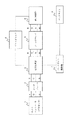
図1には本発明の一実施の形態に係るRGBW型の表示装置の構成を示し説明する。 FIG. 1 shows and describes the configuration of an RGBW display device according to an embodiment of the present invention.
この図1に示されるように、表示装置は、全体の制御を司るホストコンピュータ(プロセッサ)1、インターフェース2、信号処理部3、ゲートドライバ4、ソースドライバ5、表示画素部6、バックライト制御部7、バックライト8を備えている。
As shown in FIG. 1, the display device includes a host computer (processor) 1 that controls the whole, an interface 2, a
このような構成において、アプリケーションプロセッサ等のホストコンピュータ1やインターフェース2、信号処理部3等は、集積回路(IC;Integrated Circuit)の一部をなす。そして、ホストコンピュータ1は、入力画像信号であるR(Red),G(Green),B(Blue),W(White)信号を、インターフェース2を介して信号処理部3に送出する。
In such a configuration, the host computer 1 such as an application processor, the interface 2, the
このホストコントローラ1から送出されたRGB信号は、信号処理部3でRGBW信号に変換された後、各部に出力される。同時に、垂直および水平同期信号とバックライト制御信号等の制御信号も出力され、これらの制御信号を用いて、表示装置はRGBW画像を表示する。即ち、信号処理部3は、ゲートドライバ4、ソースドライバ5、バックライト制御部7に対して、制御信号を供給することになる。
The RGB signal transmitted from the host controller 1 is converted into an RGBW signal by the
この制御信号に基づいて、ゲートドライバ4は、表示画素部6の画素のトランジスタ(TFT;thin film transistor)をオン/オフ制御する。ソースドライバ5は、この信号処理部3からの制御信号に基づいて、その保持部に画像信号としてのR,G,B,Wのデジタル信号を保持し、順次に表示画素部6に出力する。そして、バックライト制御部7は、信号処理部3からの制御信号に基づいて、バックライト8を駆動制御する。
Based on this control signal, the gate driver 4 performs on / off control of a pixel transistor (TFT; thin film transistor) of the display pixel unit 6. Based on the control signal from the
表示画素部6は、例えば水平方向にm(m=1,2,…)個、及び垂直方向にn(n=1,2,…)個のm×n個からなる画素がマトリクス状に配置された液晶表示素子(LCD;Liquid Crystal Display)である。表示画素部6は、バックライト制御部7の制御に基づいてバックライト8から射出される光の透過率を液晶層で変化させることにより、所定の情報を画像として表示することが可能となっている。
The display pixel unit 6 includes, for example, m (m = 1, 2,...) Pixels in the horizontal direction and n (n = 1, 2,...) M × n pixels arranged in a matrix in the vertical direction. The liquid crystal display element (LCD; Liquid Crystal Display). The display pixel unit 6 can display predetermined information as an image by changing the transmittance of light emitted from the
表示解像度の単位としての1画素は、R(Red),G(Green),B(Blue),W(White)の4画素から構成されている。以下では、RGBの3画素、更にはW画素からなる表示解像度の単位としての画素を「ピクセル」と称し、該ピクセルを構成するRGBWの各画素を「サブピクセル」と称する。RGBのサブピクセルに対応する部分には赤、緑、青の半透明のカラーフィルタが配置され、Wのサブピクセルに対応する部分には透明フィルタが配置される。 One pixel as a unit of display resolution is composed of four pixels of R (Red), G (Green), B (Blue), and W (White). Hereinafter, a pixel as a unit of display resolution composed of three RGB pixels and further W pixels is referred to as a “pixel”, and each RGBW pixel constituting the pixel is referred to as a “sub-pixel”. Translucent color filters of red, green, and blue are arranged in the portion corresponding to the RGB subpixel, and transparent filters are arranged in the portion corresponding to the W subpixel.
次に図2及び図3には、表示装置のピクセルの配列例を示し説明する。 Next, FIG. 2 and FIG. 3 show an example of pixel arrangement of the display device.
即ち、図2にはピクセルがストライプ状に配列(以下、ストライプ配列という)された様子を示し、図3にはピクセルがモザイク状に配列(以下、モザイク配列という)された様子を示している。ストライプ配列では、水平方向に対してRGBWのサブピクセルを順次に配列しており、各色のサブピクセルの位置は垂直方向で同一となっている。 That is, FIG. 2 shows a state in which pixels are arranged in a stripe shape (hereinafter referred to as a stripe arrangement), and FIG. 3 shows a state in which pixels are arranged in a mosaic shape (hereinafter referred to as a mosaic arrangement). In the stripe arrangement, RGBW sub-pixels are sequentially arranged in the horizontal direction, and the positions of the sub-pixels of each color are the same in the vertical direction.
これに対して、モザイク配列では、N番目のラインではR,Wのサブピクセルが順次に配列され、N+1番目のラインではG,Bのサブピクセルが順次に配列されている。即ち、換言すれば、モザイク配列では、N番目のラインのR,WのサブピクセルとN+1番目のラインのG,Bのサブピクセルによりピクセルを構成する。 On the other hand, in the mosaic arrangement, the R and W subpixels are sequentially arranged on the Nth line, and the G and B subpixels are sequentially arranged on the N + 1th line. That is, in other words, in the mosaic arrangement, a pixel is composed of the R and W subpixels of the Nth line and the G and B subpixels of the N + 1th line.
尚、一般的には、ストライプ配列は、パーソナルコンピュータ等においてデータや文字列を表示するのに好適である。これに対して、モザイク配列は、カムコーダやデジタルスチルカメラ等において自然画を表示するのに好適である。 In general, the stripe arrangement is suitable for displaying data and character strings on a personal computer or the like. In contrast, the mosaic arrangement is suitable for displaying a natural image on a camcorder, a digital still camera, or the like.
次に、信号処理部3の詳細について説明する。
Next, details of the
本実施の形態が採用する信号処理部3についての理解を深めるべく、先ずは一般的な信号処理部10の構成、及び信号処理の流れを概説する。
In order to deepen the understanding of the
図4は、一般的な信号処理部10の構成を示すブロック図である。
FIG. 4 is a block diagram illustrating a configuration of a general
この図4に示されるように、信号処理部10は、フレームメモリ10a、ガンマ処理部10b、画像解析及びRGBW変換部(以下、画像解析部と略記する)10c、逆ガンマ処理部10dからなる。
As shown in FIG. 4, the
このような構成において、インターフェース2を通じて送られてきたRGB画像信号は一時的にフレームメモリ10aに格納される。該フレームメモリ10aに蓄積された画像情報はガンマ処理部10bへ送出され、階調―輝度特性が直線関係になるように演算されR’G’B’信号として出力される。次に画像解析部10cが画像情報を解析し、RGBW変換に必要な情報を読み出し、該情報を用いてR’G’B’信号を順次R’’G’’B’’W’’信号へと変換して出力する。このR’’G’’B’’W’’信号は、逆ガンマ処理部10dで再び逆ガンマ特性を持つように演算処理されRGBW信号として表示画素部6に送られる。
In such a configuration, the RGB image signal transmitted through the interface 2 is temporarily stored in the frame memory 10a. The image information stored in the frame memory 10a is sent to the gamma processing unit 10b, calculated so that the gradation-luminance characteristics have a linear relationship, and output as an R'G'B 'signal. Next, the
これに対して、本発明の一実施の形態に係る表示装置が採用する信号処理部3の構成は図5に示される通りである。
On the other hand, the configuration of the
即ち、この図5に示されるように、信号処理部3は、ガンマ処理部3a、画像解析およびRGBW変換部(以下、画像解析部と略記する)3b、逆ガンマ処理部3c、そして画像解析情報保持部3dからなる。
That is, as shown in FIG. 5, the
このような構成において、インターフェース2を介して送出されてきたRGB画像信号はフレームメモリを介することなく、ガンマ処理部3aへと送られる。ガンマ処理部3aにおいて、階調―輝度特性が直線関係になるように演算されR’G’B’信号として出力される。続いて、画像解析部3bでは、R’G’B’信号を解析し、RGBW変換に必要な情報を読み出し、画像解析情報保持部3dに蓄積する。即ち、画像解析情報保持部3dには、送られてきたR’G’B’信号の解析の結果、RGBW変換に必要な情報が常に保持される。
In such a configuration, the RGB image signal sent through the interface 2 is sent to the gamma processing unit 3a without going through the frame memory. In the gamma processing unit 3a, the gradation-luminance characteristics are calculated so as to have a linear relationship, and output as an R'G'B 'signal. Subsequently, the image analysis unit 3b analyzes the R'G'B 'signal, reads information necessary for RGBW conversion, and stores the information in the image analysis
ところで、リアルタイムにガンマ処理部3aから送られてきたR’G’B’信号を解析して、これらR’G’B’信号を基にRGBW変換しようとすると、本構成ではフレームメモリを持たないことから、時間的に間に合わず、従来の如き変換は不可能である。 By the way, if the R'G'B 'signal sent from the gamma processing unit 3a in real time is analyzed and RGBW conversion is attempted based on these R'G'B' signals, this configuration does not have a frame memory. For this reason, the conventional conversion is not possible in time and is impossible.
しかしながら、画像解析情報保持部3dには、先のフレームの画像解析情報が保持されている。この画像解析情報を基にRGBW変換を行なうことができる。従って、フレームメモリに蓄積することなく、送られてきたRGB信号をリアルタイムにRGBW信号へと変換することができる。この変換されたRGBW信号(即ち、R’’G’’B’’W’’信号)は、逆ガンマ処理部3cに送出される。逆ガンマ処理部3cでは、再び逆ガンマ特性を持つように演算処理され、RGBW信号として表示画素部6に送出される。
However, the image analysis
尚、以上の解析、変換処理は変調処理に相当するものである。 The above analysis and conversion process corresponds to the modulation process.
以上説明したように、信号処理部3では、RGB信号を所定の変調レベルに従って変調することで元の画像と異なる明るさに変調し、同時に光源の明るさを変調する。このとき変調レベルを決定するためのRGB信号と、変調処理をして表示画素部6にて表示を行う入力画像信号が異なるフレームのものである。また、信号処理部3は、前フレームのRGB信号で変調レベルを決定し、その結果を用いて後のフレームのRGB信号を変調する。この変調レベルの決定をRGB信号のフレーム毎に行ってもよい。
As described above, the
ここで、このような構成を採用する場合、先のフレームの画像情報が、いま送られてきた画像情報と大きく異なる場合、RGBW信号への変換が適切でない場合も考えられる。しかしながら、例えばフレーム周波数が60Hzの表示装置では、16.7msec.毎に画像解析情報が更新されるが、実際に表示されている画像が16.7msec毎に大きく変化していく例は考えられない。通常は、例えばテレビジョン(TV)や映画などの画像では、フレーム毎の画像情報の変化は少なく、なだらかに情報は変化してゆく。さらに、静止画の場合は変化がほとんどなく、複数フレームに渡って常に同じ情報が表示され続ける。 Here, when such a configuration is adopted, when the image information of the previous frame is greatly different from the image information sent now, the conversion to the RGBW signal may not be appropriate. However, for example, in a display device with a frame frequency of 60 Hz, the image analysis information is updated every 16.7 msec. However, an example in which the actually displayed image changes greatly every 16.7 msec cannot be considered. Usually, for example, in an image such as a television (TV) or a movie, the image information changes little for each frame, and the information changes gradually. Furthermore, in the case of a still image, there is almost no change, and the same information is always displayed over a plurality of frames.
従って、本実施の形態のように、先のフレームの画像解析情報を用いてRGBW信号に変換をしても問題とはならない。一瞬、画像情報が大きく変わる場合であっても、16.7msecの出来事であり、次の16.7msec後には問題とならないRGBW変換になれば人間の目には認識することは不可能である。更には、近年、画像表示装置は動画の表示品位を向上させるためにフレーム周波数を大きくする傾向があり、例えば液晶表示を用いたテレビでは120Hz程度の周波数で表示を行なっている。このような場合は、フレーム毎の情報変化は更に小さくなるため、先のフレーム情報を用いる変換の手法が有効となる。 Therefore, as in the present embodiment, there is no problem even if the image analysis information of the previous frame is used to convert the RGBW signal. Even if the image information changes greatly for a moment, it is an event of 16.7 msec, and after the next 16.7 msec, if it becomes RGBW conversion that does not cause a problem, it cannot be recognized by the human eye. Furthermore, in recent years, image display devices tend to increase the frame frequency in order to improve the display quality of moving images. For example, televisions using a liquid crystal display display at a frequency of about 120 Hz. In such a case, since the information change for each frame is further reduced, the conversion method using the previous frame information is effective.
次に、RGBWへの信号処理の基本原理を説明する。 Next, the basic principle of signal processing to RGBW will be described.
表示画素部(パネル)6に入力される画像信号がRGBのデジタル信号である場合、各色の信号レベルをRi, Gi, Biとすると、例えば各色8bitの場合はRi, Gi, Biは0から255の整数値となる。 When the image signal input to the display pixel unit (panel) 6 is an RGB digital signal, assuming that the signal level of each color is Ri, Gi, Bi, for example, when the color is 8 bits, Ri, Gi, Bi is 0 to 255. The integer value of
一方、RGBWの画素に表示するための各色の信号をRo, Go, Bo, Woとすると、表示映像の画質が変化しないようにするためには、次の関係を満たすことが必要となる。
Ri:Gi:Bi = Ro+Wo:Go+Wo:Bo+Wo
On the other hand, if each color signal to be displayed on the RGBW pixels is Ro, Go, Bo, Wo, the following relationship must be satisfied in order to prevent the image quality of the display image from changing.
Ri: Gi: Bi = Ro + Wo: Go + Wo: Bo + Wo
いま、Ri,Gi,Biの信号の最大値をMax(Ri,Gi,Bi)とすると、
Ri/Max(Ri,Gi,Bi) = (Ro+Wo)/(Max(Ri,Gi,Bi)+Wo)
Gi/Max(Ri,Gi,Bi) = (Go+Wo)/(Max(Ri,Gi,Bi)+Wo)
Bi/Max(Ri,Gi,Bi) = (Bo+Wo)/(Max(Ri,Gi,Bi)+Wo)
の関係が成り立つ。
Now, assuming that the maximum value of Ri, Gi, Bi signals is Max (Ri, Gi, Bi),
Ri / Max (Ri, Gi, Bi) = (Ro + Wo) / (Max (Ri, Gi, Bi) + Wo)
Gi / Max (Ri, Gi, Bi) = (Go + Wo) / (Max (Ri, Gi, Bi) + Wo)
Bi / Max (Ri, Gi, Bi) = (Bo + Wo) / (Max (Ri, Gi, Bi) + Wo)
The relationship holds.
従って、
Ro = Ri x((Max(Ri,Gi,Bi)+Wo)/ Max(Ri,Gi,Bi)Wo
Go = Gi x((Max(Ri,Gi,Bi)+Wo)/ Max(Ri,Gi,Bi)Wo
Bo = Bi x((Max(Ri,Gi,Bi)+Wo)/ Max(Ri,Gi,Bi)Wo
となる。
Therefore,
Ro = Ri x ((Max (Ri, Gi, Bi) + Wo) / Max (Ri, Gi, Bi) Wo
Go = Gi x ((Max (Ri, Gi, Bi) + Wo) / Max (Ri, Gi, Bi) Wo
Bo = Bi x ((Max (Ri, Gi, Bi) + Wo) / Max (Ri, Gi, Bi) Wo
It becomes.
このとき印加できるWoは、Ri,Gi,Biの最小値Min(Ri, Gi, Bi)の関数として次のように定義することができる。
Wo = f(Min(Ri,Gi,Bi)
Wo that can be applied at this time can be defined as a function of the minimum value Min (Ri, Gi, Bi) of Ri, Gi, Bi as follows.
Wo = f (Min (Ri, Gi, Bi)
即ち、最も簡単な考え方では、
Wo = Min(Ri,Gi,Bi)
である。
That is, in the simplest way of thinking,
Wo = Min (Ri, Gi, Bi)
It is.
しかるに、従来の方法では、Min(Ri,Gi,Bi)=0である画像信号が存在すると、Wo=0となり、輝度は向上しないため消費電力を下げることはできない。 However, in the conventional method, if there is an image signal with Min (Ri, Gi, Bi) = 0, Wo = 0 and the luminance is not improved, so the power consumption cannot be reduced.
また、Min(Ri,Gi,Bi)が小さい値の場合、Woの値も小さくなり、輝度向上効果が小さくなる。即ち、消費電力の低減効果が小さい。 In addition, when Min (Ri, Gi, Bi) is a small value, the value of Wo is also small, and the brightness enhancement effect is small. That is, the effect of reducing power consumption is small.
さらに、上記処理は、1枚の画像の全てのピクセルに関して行う為、映像の一部が極端に明るく、他の一部が明るくならないということも起こり得る。 Furthermore, since the above processing is performed for all the pixels of one image, a part of the video may be extremely bright and the other part may not be bright.
これは、例えば彩度が低く明るい背景の中に彩度の高い、例えば単色のデータがあった場合に、背景の信号にはWoを大きく入れることができるために明るくできるが、単色データにはWoを入れることはできず、元の明るさのままとなることを意味する。 For example, if there is high-saturation, for example, single-color data in a bright background with low saturation, the background signal can be brightened because a large Wo can be entered. Wo cannot be entered, which means that the original brightness remains unchanged.
一般に、人間の色や明るさに対する感覚(即ち、視覚特性)は、周囲との相対的な明るさの差に大きく影響を受けるため、相対的に明るさが低い単色データは、非常にくすんで見えることがある。これは、所謂同時コントラスト(Simultaneous Contrast)と称されており、RGBWの表示装置における従来の大きな課題であった。 In general, human senses of color and brightness (ie visual characteristics) are greatly affected by the difference in brightness relative to the surroundings, so monochromatic data with relatively low brightness is very dull. May be visible. This is called “simultaneous contrast” and has been a big problem in the conventional RGBW display device.
そこで、本実施の形態に係る表示装置、信号処理方法では、このような課題を解決するために以下のような処理を行う。尚、この処理は、図1の表示装置において信号処理部3により実施されるものである。
Therefore, in the display device and the signal processing method according to the present embodiment, the following processing is performed in order to solve such a problem. This process is performed by the
まず、入力画像信号の伸張処理について説明する。 First, the expansion process of the input image signal will be described.
入力画像信号Ri, Gi, Biをその比を保つように伸張する。
Ri' = α x Ri
Gi' = α x Gi
Bi' = α x Bi
αは自然数
The input image signals Ri, Gi, Bi are expanded so as to maintain the ratio.
Ri '= α x Ri
Gi '= α x Gi
Bi '= α x Bi
α is a natural number
画像信号の画質を保持するためには、伸張処理は、R, G, Bの比(輝度比)を保つように行なうことが望ましい。また、入力画像信号であるRi,Gi,Bi信号の階調−輝度特性(ガンマ)を保持するように伸張することが望ましい。この点、従来型のRGB表示装置では、8bitのデジタル信号である場合、255が最大値であるので、上記の伸張処理には限界がある。特に明るい画像信号の場合、ほとんど伸張できないこともある。 In order to maintain the image quality of the image signal, it is desirable to perform the decompression process so as to maintain the ratio of R, G, and B (luminance ratio). Further, it is desirable to expand the input image signal so as to maintain the gradation-luminance characteristics (gamma) of the Ri, Gi, Bi signals. In this regard, in the conventional RGB display device, 255 is the maximum value in the case of an 8-bit digital signal, so the above expansion processing has a limit. In particular, in the case of a bright image signal, there may be a case where it cannot be expanded almost.
これに対して、本実施の形態に係る表示装置は、RGBW型であり、Wが加わり輝度のダイナミックレンジが大きくなるために表示可能な色空間が拡張される。伸張処理は、RGBとWから構成される色空間の上限値まで行う。この為、前述した伸張処理により、従来のRGBでの限界値255を超えることが可能となる。 On the other hand, the display device according to the present embodiment is of the RGBW type, and the displayable color space is expanded because W is added and the dynamic range of luminance is increased. The expansion processing is performed up to the upper limit value of the color space composed of RGB and W. For this reason, it is possible to exceed the limit value 255 in the conventional RGB by the above-described expansion processing.
例えば、W画素の明るさが、RGB画素の明るさのK倍ある場合、Woの最大値は255xKであるとみなすことがき、Ri’,Gi’,Bi’の値はRGBW色空間において、(1+K)x255までとることが可能となる。これにより、従来の問題点であった、Min(Ri,Gi,Bi) = 0もしくは小さな値のデータに対しても、輝度を向上することができるために、消費電力を低減するという効果を奏することが可能となる。 For example, if the brightness of the W pixel is K times the brightness of the RGB pixel, the maximum value of Wo can be considered to be 255xK, and the values of Ri ′, Gi ′, Bi ′ are ( It is possible to take up to 1 + K) x255. As a result, the brightness can be improved even for data of Min (Ri, Gi, Bi) = 0 or a small value, which has been a problem in the past, and the effect of reducing power consumption is achieved. It becomes possible.
ここで、図6にはRGB型の表示装置の色空間を示し、図7にはRGBW型の表示装置の色空間を示し、説明する。図6に示されるように、全ての色は、色相(H;Hue)、彩度(S;Saturation)、明度(V;Value of Brightness)により定義される座標上にプロットすることができる。色空間の一種であるHSVは、これら色相、彩度、明度という属性で定義される。色相とは赤、青、緑のような色味の違いのことをいい、イメージの違いを最も表現することが出来る属性である。彩度とは、色を表す指標の一つであり、色の鮮やかさの度合いを示す属性である。明度とは、色の明暗の度合いを示す属性であり、数値が高いほど明るい色として表現される。HSVの色空間では、色相は、Rを0度とし、反時計回りにG,Bというように1周して表す。各色に対し、グレーがどの程度だけ混ざって濁っているかを示すのが彩度であり、最も濁っている場合を0%、全く濁っていない場合を100%と表している。明度は、最も明るい場合を100%、暗い場合を0%とする。 Here, FIG. 6 shows the color space of the RGB display device, and FIG. 7 shows the color space of the RGBW display device. As shown in FIG. 6, all colors can be plotted on coordinates defined by hue (H; Hue), saturation (S; Saturation), and lightness (V; Value of Brightness). HSV, a kind of color space, is defined by these attributes of hue, saturation, and brightness. Hue refers to the difference in color such as red, blue, and green, and is the attribute that can best express the difference in image. Saturation is one of indices indicating color, and is an attribute indicating the degree of color vividness. Lightness is an attribute that indicates the degree of lightness and darkness of a color. The higher the numerical value, the brighter the color. In the HSV color space, the hue is represented by one round such as G and B in the counterclockwise direction with R being 0 degree. For each color, the saturation shows how much gray is mixed and cloudy. The most cloudy is 0% and the cloudy is 100%. The brightness is 100% for the brightest and 0% for the darkest.
一方、図7に示されるように、RGBW型の表示装置の色空間を定義する属性は、RGB型の表示装置の色空間を定義する属性と基本的には同じであるが、Wが加えられたことで、明度が拡張されている。このように、RGB表示装置とRGBW表示装置の色空間の違いは、色相(H)、彩度(S)、明度(V)で定義されるHSV色空間で表すことができる。これによると、先に図5に示したように、Wを加えることによって拡張される明度(V)のダイナミックレンジは、彩度(S)によって大きく異なることが分かる。 On the other hand, as shown in FIG. 7, the attributes that define the color space of the RGBW display device are basically the same as the attributes that define the color space of the RGB display device, but W is added. As a result, the brightness has been expanded. As described above, the difference in color space between the RGB display device and the RGBW display device can be expressed by the HSV color space defined by the hue (H), the saturation (S), and the brightness (V). According to this, as shown in FIG. 5, it can be seen that the dynamic range of the brightness (V) expanded by adding W greatly varies depending on the saturation (S).
そこで、この信号処理方法、表示装置では、上記の入力画像信号であるRi, Gi, Bi信号の伸張処理の係数αが彩度(S)によって異なることに着目して、入力画像信号であるRi, Gi, Bi信号を解析し、映像毎に伸張係数αを決めてやることで、入力映像の画質を保持したままRGBW表示装置で映像表示をすることも可能とする。 Therefore, in this signal processing method and display device, paying attention to the fact that the coefficient α of the expansion processing of the Ri, Gi, Bi signal as the input image signal differs depending on the saturation (S), the Ri as the input image signal By analyzing the, Gi and Bi signals and determining the expansion coefficient α for each image, it is possible to display the image on the RGBW display device while maintaining the image quality of the input image.
このとき、入力画像信号の解析により彩度(S)=0から最大値(8bitの場合は255)までの値毎に伸張係数αを決定することが望ましい。そこで、更に求めた伸張係数αの最小値を採用することで、画質を全く損なうことなく伸張処理を行なう。また、この第1の実施の形態の信号処理方法、表示装置では、伸張処理が入力画像のmax(R,G,B)値とHSV色空間の最大明度値Vとの比に基づいて行われる。特に、この比を彩度値 S=0から最大値まで算出し、その最小値を伸張係数として用いて伸張処理を実施する。 At this time, it is desirable to determine the expansion coefficient α for each value from saturation (S) = 0 to the maximum value (255 in the case of 8 bits) by analyzing the input image signal. Therefore, by adopting the minimum value of the obtained expansion coefficient α, the expansion process is performed without any loss of image quality. In the signal processing method and display device according to the first embodiment, the expansion process is performed based on the ratio between the max (R, G, B) value of the input image and the maximum brightness value V of the HSV color space. . In particular, this ratio is calculated from the saturation value S = 0 to the maximum value, and the expansion processing is performed using the minimum value as the expansion coefficient.
尚、画質を最大限保持するためには、入力された画像信号の全てのピクセルデータを解析することが望ましい。その一方で、処理速度を速めると共に、処理ブロックの回路規模を小さくするためには、入力画像信号をn(ここで、nは1以上の自然数である)個飛ばしで解析することが望ましい。また、入力画像信号のRGBデータのうち少なくとも1つ以上を解析することが望ましい。更には、伸張係数αの決定法として、人間工学的なアプローチを取ることも可能であることは勿論である。 In order to maintain the maximum image quality, it is desirable to analyze all pixel data of the input image signal. On the other hand, in order to increase the processing speed and reduce the circuit scale of the processing block, it is desirable to analyze by skipping n (where n is a natural number of 1 or more) input image signals. It is desirable to analyze at least one of the RGB data of the input image signal. Furthermore, it is of course possible to take an ergonomic approach as a method of determining the expansion coefficient α.
また、入力画像信号であるRi, Gi, Bi信号が局所的にわずかに変化しただけでは、人間には知覚できない。よって、伸張係数αを画質変化の知覚限界まで大きな値とすることで、画質変化を知覚することなく、大きく伸張することを可能とする。換言すれば、画質変化が知覚できない範囲で伸張処理を実施する。 In addition, humans cannot perceive if the Ri, Gi, Bi signals as input image signals are only slightly changed locally. Therefore, by setting the expansion coefficient α to a large value up to the perception limit of the image quality change, it is possible to greatly expand without perceiving the image quality change. In other words, the decompression process is performed within a range where the change in image quality cannot be perceived.
尚、図8に示されるように、伸張映像信号は、拡張されたRGBWの色空間に対して入力映像信号のレベルを比較することで決定した伸張係数αに基づいて生成される。 As shown in FIG. 8, the expanded video signal is generated based on the expansion coefficient α determined by comparing the level of the input video signal with respect to the expanded RGBW color space.
以上の方法で入力画像信号を伸張することで、Woの値を大きくとることができ、映像全体の輝度をより向上することができ、その結果としてバックライトの消費電力を大幅に低減することも可能となる。また、伸張係数αに従って、バックライトの輝度を1/αに下げることで、入力画像信号と全く同一の輝度で表示することも可能となる。 By expanding the input image signal by the above method, the value of Wo can be increased, the brightness of the entire video can be further improved, and as a result, the power consumption of the backlight can be significantly reduced. It becomes possible. Further, by reducing the luminance of the backlight to 1 / α according to the expansion coefficient α, it is possible to display with exactly the same luminance as the input image signal.
次に、伸張した画像信号Ri’,Bi’,Gi’からWoを決定する方法について述べる。 Next, a method for determining Wo from the expanded image signals Ri ', Bi', Gi 'will be described.
この実施の形態では、伸張したRGBの画像信号からX信号成分を抽出し、X信号レベルを決定する際に入力画像を解析することによってX信号レベル決定する。そして、X信号の取り得る最大値をX信号レベルとする。以下、詳述する。 In this embodiment, the X signal level is determined by extracting the X signal component from the decompressed RGB image signal and analyzing the input image when determining the X signal level. The maximum value that the X signal can take is set as the X signal level. Details will be described below.
先に述べたように、伸張した画像信号Ri’,Bi’,Bi’を解析することで各ピクセルの最小値Min(Ri’,Gi’,Bi’)を求め、Wo = Min(Ri', Gi', Bi')にすることが望ましく、これがWoの取り得る最大値となるため、消費電力低減の効果は最も高い。 As described above, the minimum value Min (Ri ′, Gi ′, Bi ′) of each pixel is obtained by analyzing the expanded image signal Ri ′, Bi ′, Bi ′, and Wo = Min (Ri ′, Gi ′, Bi ′) is desirable, and this is the maximum value that can be taken by Wo, so that the effect of reducing power consumption is the highest.
よって、Woの決定は、伸張された画像信号Ri’,Gi’,Bi’を解析し、最小値Min(Ri’,Gi’,Bi’)を求め、これをWoとするのが最も消費電力削減効果が高い。 Therefore, Wo is determined by analyzing the decompressed image signals Ri ′, Gi ′, Bi ′, obtaining the minimum value Min (Ri ′, Gi ′, Bi ′), and setting this as Wo as the most power consumption. Reduction effect is high.
上記の手法でWoを決定した結果、新たなRGBの画像信号は下記のように求められる。
Ro = Ri’ Wo
Go = Gi' Wo
Bo = Bi' Wo
As a result of determining Wo by the above method, a new RGB image signal is obtained as follows.
Ro = Ri 'Wo
Go = Gi 'Wo
Bo = Bi 'Wo
上記の方法で入力画像信号を伸張することで、Woの値を大きくとることができ、画像全体の輝度をより向上することができ、結果としてバックライトの消費電力を大幅に低減することが可能となる。伸張係数αにしたがって、バックライトの輝度を1/αに下げることで、入力画像信号と全く同一の輝度で表示することが可能となる。 By expanding the input image signal using the above method, the value of Wo can be increased, the brightness of the entire image can be further improved, and as a result, the power consumption of the backlight can be greatly reduced. It becomes. By reducing the brightness of the backlight to 1 / α according to the expansion coefficient α, it becomes possible to display with exactly the same brightness as the input image signal.
ところで、上記の伸張画像信号は、RGBWが形成する色空間に対して入力画像信号の明度レベルを比較することで決定した伸張係数αに基づいて生成される。よって、伸張係数αは1フレームの画像を解析した結果得られる画像解析情報である。これを画像解析情報保持部3dに保持しておき、次フレームの画像信号の変換に用いることで、画像信号をフレームメモリに蓄積することなく、RGBWの適切な変換を行なうことができる。変調レベルは、RGB信号の各ピクセルの最大明度値により決定される。
By the way, the above-described decompressed image signal is generated based on the decompression coefficient α determined by comparing the brightness level of the input image signal with respect to the color space formed by RGBW. Therefore, the expansion coefficient α is image analysis information obtained as a result of analyzing one frame image. By holding this in the image analysis
また、α値は入力画像信号の明度レベルと色空間との比較で決定されるため、画像情報が多少変化しても変わらない。例えば、画面の中を動き回る画像があったとしても、輝度や色度が大きく変化しなければα値は同一である。よって、先のフレームで決定されたα値を用いてRGBWの変換を行なっても全く問題ない。尚、変調処理としては、RGB信号を伸張処理することで明度を高める処理と、光源の明るさを低下させる処理がある。 Since the α value is determined by comparing the lightness level of the input image signal with the color space, it does not change even if the image information changes slightly. For example, even if there is an image that moves around the screen, the α value is the same if the luminance and chromaticity do not change greatly. Therefore, there is no problem even if RGBW conversion is performed using the α value determined in the previous frame. The modulation process includes a process for increasing the brightness by expanding the RGB signal and a process for decreasing the brightness of the light source.
以上詳述したように、本発明の一実施の形態によれば、フレームメモリを持たずに画像変換処理が可能なため、ICのサイズダウン(縮小)やコストダウンをはかりつつ、高機能で低消費電力な表示装置等を実現することができる。 As described above in detail, according to one embodiment of the present invention, since image conversion processing is possible without having a frame memory, it is possible to reduce the size and cost of the IC while reducing the cost and reducing the cost. A power consumption display device or the like can be realized.
以上、本発明の一実施の形態について説明したが、本発明はこれに限定されることなくその趣旨を逸脱しない範囲で種々の改良・変更が可能である。 Although one embodiment of the present invention has been described above, the present invention is not limited to this, and various improvements and modifications can be made without departing from the spirit of the present invention.
例えば、上記実施の形態では、RGBWの信号処理を、バックライトを有する液晶表示装置を例にとって示したが、これ以外に有機EL(Organic Electro-Luminescence)、PDP(Plasma Display Panel)、SED(Surface-conduction Electron-emitter Display)並びにCRT(Cathode Ray Tube)などの他方式の映像表示装置にも用いることができる。 For example, in the above-described embodiment, RGBW signal processing is shown by taking a liquid crystal display device having a backlight as an example. -conduction Electron-emitter Display) and other types of video display devices such as CRT (Cathode Ray Tube).
また、ピクセルをRGBのカラーフィルタが配置されたサブピクセルと発光層により構成されたWのサブピクセルにより構成してもよく、RGBWの全てのサブピクセルを発光層により構成してもよい。また、フロントライトユニットを持つ反射型表示装置にも適用が可能であるため、低消費電力が求められる電子ペーパー向けの表示装置にも好適である。 Further, the pixel may be constituted by a W subpixel formed by a subpixel in which an RGB color filter is arranged and a light emitting layer, or all the RGBW subpixels may be constituted by a light emitting layer. Further, since it can be applied to a reflective display device having a front light unit, it is also suitable for a display device for electronic paper that requires low power consumption.
さらに、上記では、RGBWを例にとって説明したが、W以外のイエロー(Yellow)やシアン(Cyan)並びにマゼンダ(Magenda)等でもよい。 Furthermore, in the above description, RGBW has been described as an example, but yellow, cyan, and magenta other than W may be used.
さらに、多板式のプロジェクタのような表示装置にも適用することにより、明るさを向上することができ、消費電力を下げることが可能である。 Furthermore, when applied to a display device such as a multi-panel projector, brightness can be improved and power consumption can be reduced.
1…ホストコントローラ、2…インターフェース、3…信号処理部、3a…ガンマ処理部、3b…画像解析およびRGBW変換部、3c…逆ガンマ処理部、3d…画像解析情報保持部、4…ゲートドライバ、5…ソースドライバ、6…表示画素部、7…バックライト制御部、8…バックライト DESCRIPTION OF SYMBOLS 1 ... Host controller, 2 ... Interface, 3 ... Signal processing part, 3a ... Gamma processing part, 3b ... Image analysis and RGBW conversion part, 3c ... Inverse gamma processing part, 3d ... Image analysis information holding part, 4 ... Gate driver, 5 ... Source driver, 6 ... Display pixel unit, 7 ... Backlight control unit, 8 ... Backlight
Claims (11)
前記入力画像信号の信号レベルを伸張し、この伸張した赤、緑、青の信号から前記所定色の信号成分を抽出し、該所定色の信号レベルを決定し、この決定された所定色の信号レベルに基づいて伸張処理を行い、この伸張処理後の赤、緑、青の信号を所定の変調レベルに従って変調することで元の画像と異なる明るさに変調し、同時に光源の明るさを変調する信号処理部とを備え、
前記変調レベルを決定するための入力画像信号と、変調処理をして前記表示画素部にて表示を行う入力画像信号が異なるフレームのものである
表示装置。 In addition to red, green, and blue, a display pixel portion in which output sub-pixels of a predetermined color are arranged to form a pixel;
The signal level of the input image signal is expanded, the signal component of the predetermined color is extracted from the expanded red, green and blue signals, the signal level of the predetermined color is determined, and the signal of the determined predetermined color The expansion process is performed based on the level, and the red, green, and blue signals after the expansion process are modulated according to a predetermined modulation level to modulate the brightness different from the original image and simultaneously modulate the brightness of the light source. A signal processing unit,
The display device, wherein the input image signal for determining the modulation level is different from the input image signal that is subjected to modulation processing and displayed on the display pixel unit.
請求項1に記載の表示装置。 The display device according to claim 1, wherein the signal processing unit determines the modulation level based on an input image signal of a previous frame, and modulates an input image signal of a subsequent frame using the result.
請求項2に記載の表示装置。 The display device according to claim 2, further comprising: an information holding unit that holds the modulation level determined by the input image signal of the previous frame as image analysis information.
請求項1に記載の表示装置。 The display device according to claim 1, wherein the signal processing unit determines the modulation level for each frame of an input image signal.
請求項1に記載の表示装置。 The display device according to claim 1, wherein the modulation level is determined by a maximum brightness value of each pixel of the input image signal.
請求項1に記載の表示装置。 The display device according to claim 1, wherein the signal processing unit performs, as the modulation processing, processing for increasing brightness by expanding an input image signal and processing for reducing brightness of a light source.
赤、緑、青の入力画像信号を所定の変調レベルに従って変調することで元の画像と異なる明るさに変調し、同時に光源の明るさを変調する信号処理部とを備え、
前記変調レベルを決定するための入力画像信号と、変調処理をして前記表示画素部にて表示を行う入力画像信号が異なるフレームのものである
表示装置。 A display pixel unit in which red, green, and blue output sub-pixels are arranged to form a pixel;
A signal processing unit that modulates red, green, and blue input image signals according to a predetermined modulation level to modulate the brightness different from the original image, and simultaneously modulates the brightness of the light source;
The display device, wherein the input image signal for determining the modulation level is different from the input image signal that is subjected to modulation processing and displayed on the display pixel unit.
表示画素部が、この変調後の信号に基づいて表示を行うステップとを備え、
前記変調レベルを決定するための入力画像信号と、変調処理をして前記表示画素部にて表示を行う入力画像信号が異なるフレームのものである
表示装置の駆動方法。 A signal processor that modulates red, green, and blue input image signals according to a predetermined modulation level to modulate the brightness different from the original image, and simultaneously modulates the brightness of the light source;
A display pixel unit including a step of performing display based on the modulated signal,
The method for driving a display device, wherein the input image signal for determining the modulation level and the input image signal for performing modulation processing and displaying on the display pixel unit are different frames.
前記変調レベルを決定するための入力画像信号と、変調処理をして前記表示画素部にて表示を行う入力画像信号が異なるフレームのものである
駆動用集積回路。 A signal processing unit that modulates red, green, and blue input image signals according to a predetermined modulation level to modulate the brightness different from the original image, and simultaneously modulates the brightness of the light source;
An integrated circuit for driving, wherein the input image signal for determining the modulation level and the input image signal that is subjected to modulation processing and displayed on the display pixel portion are of different frames.
この変調後の信号に基づいて表示画素部に表示を行うステップとを備え、
前記変調レベルを決定するための入力画像信号と、変調処理をして前記表示画素部にて表示を行う入力画像信号が異なるフレームのものである
駆動用集積回路による駆動方法。 A signal processor that modulates red, green, and blue input image signals according to a predetermined modulation level to modulate the brightness different from the original image, and simultaneously modulates the brightness of the light source;
And displaying on the display pixel portion based on the modulated signal,
A driving method using an integrated circuit for driving, wherein the input image signal for determining the modulation level and the input image signal for performing modulation processing and displaying on the display pixel portion are of different frames.
前記変調レベルを決定するための入力画像信号と、変調処理をして表示を行う入力画像信号が異なるフレームのものである
信号処理方法。 By modulating the input image signal of red, green and blue according to the predetermined modulation level, it modulates to the brightness different from the original image, and simultaneously modulates the brightness of the light source,
The signal processing method, wherein the input image signal for determining the modulation level is different from the input image signal to be displayed after modulation processing.
Priority Applications (5)
| Application Number | Priority Date | Filing Date | Title |
|---|---|---|---|
| JP2008183033A JP2010020241A (en) | 2008-07-14 | 2008-07-14 | Display apparatus, method of driving display apparatus, drive-use integrated circuit, driving method employed by drive-use integrated circuit, and signal processing method |
| US12/457,451 US8743152B2 (en) | 2008-07-14 | 2009-06-11 | Display apparatus, method of driving display apparatus, drive-use integrated circuit, driving method employed by drive-use integrated circuit, and signal processing method |
| TW098120144A TWI413098B (en) | 2008-07-14 | 2009-06-16 | Display apparatus |
| KR1020090062014A KR20100007748A (en) | 2008-07-14 | 2009-07-08 | Display apparatus, method of driving display apparatus, drive-use integrated circuit, driving method employed by drive-use integrated circuit, and signal processing method |
| CN200910152273.7A CN101630498B (en) | 2008-07-14 | 2009-07-14 | Display apparatus, method of driving display apparatus, drive-use integrated circuit, and signal processing method |
Applications Claiming Priority (1)
| Application Number | Priority Date | Filing Date | Title |
|---|---|---|---|
| JP2008183033A JP2010020241A (en) | 2008-07-14 | 2008-07-14 | Display apparatus, method of driving display apparatus, drive-use integrated circuit, driving method employed by drive-use integrated circuit, and signal processing method |
Publications (1)
| Publication Number | Publication Date |
|---|---|
| JP2010020241A true JP2010020241A (en) | 2010-01-28 |
Family
ID=41504761
Family Applications (1)
| Application Number | Title | Priority Date | Filing Date |
|---|---|---|---|
| JP2008183033A Pending JP2010020241A (en) | 2008-07-14 | 2008-07-14 | Display apparatus, method of driving display apparatus, drive-use integrated circuit, driving method employed by drive-use integrated circuit, and signal processing method |
Country Status (5)
| Country | Link |
|---|---|
| US (1) | US8743152B2 (en) |
| JP (1) | JP2010020241A (en) |
| KR (1) | KR20100007748A (en) |
| CN (1) | CN101630498B (en) |
| TW (1) | TWI413098B (en) |
Cited By (16)
| Publication number | Priority date | Publication date | Assignee | Title |
|---|---|---|---|---|
| JP2010033009A (en) * | 2008-06-23 | 2010-02-12 | Sony Corp | Image display device, driving method thereof, image display device assembly, and driving method thereof |
| JP2012028964A (en) * | 2010-07-22 | 2012-02-09 | Seiko Epson Corp | Image display device, image supply device, and image processing method |
| JP2012028963A (en) * | 2010-07-22 | 2012-02-09 | Seiko Epson Corp | Image display device, image display method, and image supply device |
| JP2012028965A (en) * | 2010-07-22 | 2012-02-09 | Seiko Epson Corp | Image display device, image supply device, and image processing method |
| JP2012108518A (en) * | 2008-06-23 | 2012-06-07 | Sony Mobile Display Corp | Image display device and method for driving the same and image display device assembly and method for driving the same |
| JP2014139647A (en) * | 2012-12-19 | 2014-07-31 | Japan Display Inc | Display device, driving method of display device, and electronic apparatus |
| JP2015082020A (en) * | 2013-10-22 | 2015-04-27 | 株式会社ジャパンディスプレイ | Display device, electronic apparatus, and driving method of display device |
| JP2015203798A (en) * | 2014-04-15 | 2015-11-16 | 株式会社ジャパンディスプレイ | Display device and display method |
| JP2015210389A (en) * | 2014-04-25 | 2015-11-24 | 株式会社ジャパンディスプレイ | Display device, display device driving method, and electronic apparatus |
| JP2016006482A (en) * | 2014-05-27 | 2016-01-14 | Nltテクノロジー株式会社 | Control signal generation circuit, video display device, control signal generation method, and program thereof |
| JP2016114789A (en) * | 2014-12-15 | 2016-06-23 | 株式会社ジャパンディスプレイ | Display device and color conversion method |
| US9552758B2 (en) | 2014-05-23 | 2017-01-24 | Japan Display Inc. | Display device and image processing device |
| US9646528B2 (en) | 2014-07-22 | 2017-05-09 | Japan Display Inc. | Image display device and method of displaying image |
| US9653041B2 (en) | 2014-07-22 | 2017-05-16 | Japan Display Inc. | Image display device and method of displaying image |
| US9704426B2 (en) | 2014-05-23 | 2017-07-11 | Japan Display Inc. | Display device, display system, and image processing circuit |
| US9852710B2 (en) | 2014-07-22 | 2017-12-26 | Japan Display Inc. | Image display device and method of displaying image |
Families Citing this family (26)
| Publication number | Priority date | Publication date | Assignee | Title |
|---|---|---|---|---|
| JP5404546B2 (en) * | 2010-07-16 | 2014-02-05 | 株式会社ジャパンディスプレイ | Driving method of image display device |
| JP5481323B2 (en) * | 2010-09-01 | 2014-04-23 | 株式会社ジャパンディスプレイ | Driving method of image display device |
| US20130194170A1 (en) * | 2010-10-19 | 2013-08-01 | Sharp Kabushiki Kaisha | Display device |
| US9183789B2 (en) * | 2011-04-07 | 2015-11-10 | Sharp Kabushiki Kaisha | Display device, and brightness control signal generation method |
| US8824793B2 (en) | 2012-03-02 | 2014-09-02 | Adobe Systems Incorporated | Methods and apparatus for applying a bokeh effect to images |
| JP6167324B2 (en) * | 2012-07-25 | 2017-07-26 | 株式会社Joled | Display device, image processing device, and image processing method |
| KR101384993B1 (en) | 2012-09-27 | 2014-04-14 | 삼성디스플레이 주식회사 | Method of opperating an organic light emitting display device, and organic light emitting display device |
| JP5780259B2 (en) * | 2013-03-26 | 2015-09-16 | ソニー株式会社 | Information processing apparatus, information processing method, and program |
| US20150062201A1 (en) * | 2013-08-27 | 2015-03-05 | Boe Technology Group Co., Ltd. | Display device |
| US9230345B2 (en) * | 2013-10-02 | 2016-01-05 | Pixtronix, Inc. | Display apparatus configured for display of lower resolution composite color subfields |
| CN103927999B (en) * | 2013-12-30 | 2017-03-08 | 上海天马微电子有限公司 | Driving method and driving circuit of display and display device |
| CN103854570B (en) * | 2014-02-20 | 2016-08-17 | 北京京东方光电科技有限公司 | Display base plate and driving method thereof and display device |
| JP6439418B2 (en) * | 2014-03-05 | 2018-12-19 | ソニー株式会社 | Image processing apparatus, image processing method, and image display apparatus |
| JP2015194747A (en) | 2014-03-27 | 2015-11-05 | 株式会社ジャパンディスプレイ | Display device and driving method of display device |
| JP2015210388A (en) | 2014-04-25 | 2015-11-24 | 株式会社ジャパンディスプレイ | Display device |
| CN104410849B (en) * | 2014-10-21 | 2016-06-29 | 深圳市华星光电技术有限公司 | Image processing method and device |
| KR102194571B1 (en) * | 2014-10-23 | 2020-12-24 | 엘지디스플레이 주식회사 | Method of data conversion and data converter |
| JP6399933B2 (en) * | 2015-01-06 | 2018-10-03 | 株式会社ジャパンディスプレイ | Display device and driving method of display device |
| JP6450195B2 (en) * | 2015-01-08 | 2019-01-09 | 株式会社ジャパンディスプレイ | Display device and electronic device |
| KR102587865B1 (en) * | 2016-11-30 | 2023-10-10 | 엘지디스플레이 주식회사 | Display device and image processing method thereof |
| CN109891486B (en) * | 2017-09-12 | 2023-04-25 | 索尼公司 | Display device and signal processing device |
| CN107742507B (en) * | 2017-10-31 | 2019-11-22 | 武汉华星光电技术有限公司 | Improve the method and system of display color gamut |
| JP7455521B2 (en) * | 2019-06-20 | 2024-03-26 | エルジー ディスプレイ カンパニー リミテッド | Display control device, display device, and display control method |
| CN111277810A (en) | 2020-01-22 | 2020-06-12 | 合肥鑫晟光电科技有限公司 | Image processing method, image processing module and display device |
| KR20230032704A (en) * | 2021-08-31 | 2023-03-07 | 삼성전자주식회사 | Display device and operating method for the same |
| CN117642768A (en) | 2021-08-31 | 2024-03-01 | 三星电子株式会社 | Display devices and methods of operation |
Citations (12)
| Publication number | Priority date | Publication date | Assignee | Title |
|---|---|---|---|---|
| JPH11146209A (en) * | 1997-11-12 | 1999-05-28 | Sharp Corp | Color reproduction method |
| JP2001144975A (en) * | 1999-11-10 | 2001-05-25 | Seiko Epson Corp | Color conversion method, color conversion device, and recording medium |
| JP2002024268A (en) * | 2000-06-12 | 2002-01-25 | Internatl Business Mach Corp <Ibm> | Method for retrieving and ranking document from database, computer system, and recording medium |
| JP2002132225A (en) * | 2000-10-24 | 2002-05-09 | Sharp Corp | Video signal correction device and multimedia computer system using the same |
| JP2003244458A (en) * | 2002-02-15 | 2003-08-29 | Mitsubishi Electric Corp | Image display device and color conversion method |
| JP2006163069A (en) * | 2004-12-08 | 2006-06-22 | Sanyo Electric Co Ltd | Signal processing circuit and signal processing method for self-luminous display device |
| JP2006317899A (en) * | 2005-05-12 | 2006-11-24 | Lg Philips Lcd Co Ltd | Driving device and driving method for liquid crystal display device |
| WO2007004194A2 (en) * | 2005-07-05 | 2007-01-11 | Koninklijke Philips Electronics N.V. | Method and apparatus for converting colour signals for driving an rgbw display and a display using the same |
| JP2007010753A (en) * | 2005-06-28 | 2007-01-18 | Hitachi Displays Ltd | Liquid crystal display |
| JP2007212834A (en) * | 2006-02-10 | 2007-08-23 | Seiko Epson Corp | Image display method and apparatus |
| JP2008026339A (en) * | 2004-12-24 | 2008-02-07 | Sharp Corp | Display device |
| JP2008107715A (en) * | 2006-10-27 | 2008-05-08 | Seiko Epson Corp | Image display device, image display method, image display program, recording medium storing image display program, and electronic apparatus |
Family Cites Families (9)
| Publication number | Priority date | Publication date | Assignee | Title |
|---|---|---|---|---|
| JPH07129113A (en) | 1993-10-29 | 1995-05-19 | Sharp Corp | Display device for adjusting display brightness |
| JP2003022053A (en) * | 2001-07-05 | 2003-01-24 | Sony Corp | Image display device and image display method |
| US6897876B2 (en) | 2003-06-26 | 2005-05-24 | Eastman Kodak Company | Method for transforming three color input signals to four or more output signals for a color display |
| JP4529553B2 (en) * | 2004-06-17 | 2010-08-25 | 船井電機株式会社 | Multi-display control apparatus and multi-display control method |
| TW200623001A (en) * | 2004-12-31 | 2006-07-01 | Wintek Corp | Image-processing device and method for enhancing the luminance and the image quality of display panels |
| KR20070014862A (en) | 2005-07-29 | 2007-02-01 | 삼성전자주식회사 | Image signal processing device, liquid crystal display device and driving method thereof |
| KR100760943B1 (en) * | 2006-01-25 | 2007-09-21 | 엘지.필립스 엘시디 주식회사 | Driving device and driving method of mobile display device |
| CN101079227A (en) * | 2006-05-26 | 2007-11-28 | 奇美电子股份有限公司 | Driving method of pixel level multitasking architecture and device using the method |
| US7592996B2 (en) * | 2006-06-02 | 2009-09-22 | Samsung Electronics Co., Ltd. | Multiprimary color display with dynamic gamut mapping |
-
2008
- 2008-07-14 JP JP2008183033A patent/JP2010020241A/en active Pending
-
2009
- 2009-06-11 US US12/457,451 patent/US8743152B2/en active Active
- 2009-06-16 TW TW098120144A patent/TWI413098B/en active
- 2009-07-08 KR KR1020090062014A patent/KR20100007748A/en not_active Ceased
- 2009-07-14 CN CN200910152273.7A patent/CN101630498B/en active Active
Patent Citations (12)
| Publication number | Priority date | Publication date | Assignee | Title |
|---|---|---|---|---|
| JPH11146209A (en) * | 1997-11-12 | 1999-05-28 | Sharp Corp | Color reproduction method |
| JP2001144975A (en) * | 1999-11-10 | 2001-05-25 | Seiko Epson Corp | Color conversion method, color conversion device, and recording medium |
| JP2002024268A (en) * | 2000-06-12 | 2002-01-25 | Internatl Business Mach Corp <Ibm> | Method for retrieving and ranking document from database, computer system, and recording medium |
| JP2002132225A (en) * | 2000-10-24 | 2002-05-09 | Sharp Corp | Video signal correction device and multimedia computer system using the same |
| JP2003244458A (en) * | 2002-02-15 | 2003-08-29 | Mitsubishi Electric Corp | Image display device and color conversion method |
| JP2006163069A (en) * | 2004-12-08 | 2006-06-22 | Sanyo Electric Co Ltd | Signal processing circuit and signal processing method for self-luminous display device |
| JP2008026339A (en) * | 2004-12-24 | 2008-02-07 | Sharp Corp | Display device |
| JP2006317899A (en) * | 2005-05-12 | 2006-11-24 | Lg Philips Lcd Co Ltd | Driving device and driving method for liquid crystal display device |
| JP2007010753A (en) * | 2005-06-28 | 2007-01-18 | Hitachi Displays Ltd | Liquid crystal display |
| WO2007004194A2 (en) * | 2005-07-05 | 2007-01-11 | Koninklijke Philips Electronics N.V. | Method and apparatus for converting colour signals for driving an rgbw display and a display using the same |
| JP2007212834A (en) * | 2006-02-10 | 2007-08-23 | Seiko Epson Corp | Image display method and apparatus |
| JP2008107715A (en) * | 2006-10-27 | 2008-05-08 | Seiko Epson Corp | Image display device, image display method, image display program, recording medium storing image display program, and electronic apparatus |
Cited By (23)
| Publication number | Priority date | Publication date | Assignee | Title |
|---|---|---|---|---|
| US8194094B2 (en) | 2008-06-23 | 2012-06-05 | Sony Corporation | Image display apparatus and driving method thereof, and image display apparatus assembly and driving method thereof |
| JP2012108518A (en) * | 2008-06-23 | 2012-06-07 | Sony Mobile Display Corp | Image display device and method for driving the same and image display device assembly and method for driving the same |
| US8432412B2 (en) | 2008-06-23 | 2013-04-30 | Sony Corporation | Image display apparatus and driving method thereof, and image display apparatus assembly and driving method thereof |
| JP2010033009A (en) * | 2008-06-23 | 2010-02-12 | Sony Corp | Image display device, driving method thereof, image display device assembly, and driving method thereof |
| JP2012028964A (en) * | 2010-07-22 | 2012-02-09 | Seiko Epson Corp | Image display device, image supply device, and image processing method |
| JP2012028963A (en) * | 2010-07-22 | 2012-02-09 | Seiko Epson Corp | Image display device, image display method, and image supply device |
| JP2012028965A (en) * | 2010-07-22 | 2012-02-09 | Seiko Epson Corp | Image display device, image supply device, and image processing method |
| US9324283B2 (en) | 2012-12-19 | 2016-04-26 | Japan Display Inc. | Display device, driving method of display device, and electronic apparatus |
| JP2014139647A (en) * | 2012-12-19 | 2014-07-31 | Japan Display Inc | Display device, driving method of display device, and electronic apparatus |
| JP2015082020A (en) * | 2013-10-22 | 2015-04-27 | 株式会社ジャパンディスプレイ | Display device, electronic apparatus, and driving method of display device |
| JP2015203798A (en) * | 2014-04-15 | 2015-11-16 | 株式会社ジャパンディスプレイ | Display device and display method |
| JP2015210389A (en) * | 2014-04-25 | 2015-11-24 | 株式会社ジャパンディスプレイ | Display device, display device driving method, and electronic apparatus |
| US9552758B2 (en) | 2014-05-23 | 2017-01-24 | Japan Display Inc. | Display device and image processing device |
| US9704426B2 (en) | 2014-05-23 | 2017-07-11 | Japan Display Inc. | Display device, display system, and image processing circuit |
| CN105280146A (en) * | 2014-05-27 | 2016-01-27 | Nlt科技股份有限公司 | Control signal generation circuit, video display device, and control signal generation method |
| JP2016006482A (en) * | 2014-05-27 | 2016-01-14 | Nltテクノロジー株式会社 | Control signal generation circuit, video display device, control signal generation method, and program thereof |
| US9711112B2 (en) | 2014-05-27 | 2017-07-18 | Nlt Technologies, Ltd. | Control signal generation circuit and control signal generation method for controlling luminance in a display device |
| US9646528B2 (en) | 2014-07-22 | 2017-05-09 | Japan Display Inc. | Image display device and method of displaying image |
| US9653041B2 (en) | 2014-07-22 | 2017-05-16 | Japan Display Inc. | Image display device and method of displaying image |
| US9852710B2 (en) | 2014-07-22 | 2017-12-26 | Japan Display Inc. | Image display device and method of displaying image |
| US10235966B2 (en) | 2014-07-22 | 2019-03-19 | Japan Display Inc. | Image display device and method of displaying image |
| US10672364B2 (en) | 2014-07-22 | 2020-06-02 | Japan Display Inc. | Image display device and method of displaying image |
| JP2016114789A (en) * | 2014-12-15 | 2016-06-23 | 株式会社ジャパンディスプレイ | Display device and color conversion method |
Also Published As
| Publication number | Publication date |
|---|---|
| KR20100007748A (en) | 2010-01-22 |
| US20100007679A1 (en) | 2010-01-14 |
| CN101630498A (en) | 2010-01-20 |
| TW201013632A (en) | 2010-04-01 |
| US8743152B2 (en) | 2014-06-03 |
| TWI413098B (en) | 2013-10-21 |
| CN101630498B (en) | 2014-09-10 |
Similar Documents
| Publication | Publication Date | Title |
|---|---|---|
| JP2010020241A (en) | Display apparatus, method of driving display apparatus, drive-use integrated circuit, driving method employed by drive-use integrated circuit, and signal processing method | |
| JP5430068B2 (en) | Display device | |
| JP5963933B2 (en) | Signal conversion apparatus and method, program, and recording medium | |
| CN101256759B (en) | Backlight unit and method | |
| CN105280146B (en) | Control signal generating circuit, video display devices and control signal creating method | |
| CN105609032B (en) | Data cutting method and the display device for using data cutting method | |
| CN106560880B (en) | The image rendering method of display device and the display device | |
| CN106531046A (en) | Display device | |
| JP2014139647A (en) | Display device, driving method of display device, and electronic apparatus | |
| JP2005107491A (en) | Liquid crystal display device and driving method thereof | |
| KR20110012685A (en) | Data correction method and liquid crystal display device using the same | |
| CN104471922A (en) | Display device | |
| US11605358B2 (en) | Liquid crystal display including two overlapping display panels that differ from each other in terms of the size of their respective display pixels | |
| US9953558B1 (en) | Transparent display apparatus and method for driving transparent display panel thereof | |
| US9311886B2 (en) | Display device including signal processing unit that converts an input signal for an input HSV color space, electronic apparatus including the display device, and drive method for the display device | |
| US11386869B2 (en) | Display device and driving method thereof according to capturing conditions of an image | |
| KR102227478B1 (en) | Display controlling apparatus, display controlling method, and display apparatus | |
| JP6551230B2 (en) | Signal generation device and image display device | |
| US9734772B2 (en) | Display device | |
| US9569999B2 (en) | Signal generation apparatus, signal generation program, signal generation method, and image display apparatus | |
| JP2010048958A (en) | Image processing device, processing method therefor and image display system | |
| CN103886824A (en) | Transparent display device and method of driving the same | |
| US9704426B2 (en) | Display device, display system, and image processing circuit | |
| WO2012137753A1 (en) | Display device and control method of display device | |
| JP2015220721A (en) | Display device, image signal processing device and image signal processing method |
Legal Events
| Date | Code | Title | Description |
|---|---|---|---|
| A977 | Report on retrieval |
Free format text: JAPANESE INTERMEDIATE CODE: A971007 Effective date: 20100426 |
|
| A131 | Notification of reasons for refusal |
Free format text: JAPANESE INTERMEDIATE CODE: A131 Effective date: 20100506 |
|
| A521 | Written amendment |
Free format text: JAPANESE INTERMEDIATE CODE: A523 Effective date: 20100705 |
|
| A131 | Notification of reasons for refusal |
Free format text: JAPANESE INTERMEDIATE CODE: A131 Effective date: 20110526 |
|
| A521 | Written amendment |
Free format text: JAPANESE INTERMEDIATE CODE: A523 Effective date: 20110725 |
|
| A02 | Decision of refusal |
Free format text: JAPANESE INTERMEDIATE CODE: A02 Effective date: 20110811 |
|
| A521 | Written amendment |
Free format text: JAPANESE INTERMEDIATE CODE: A523 Effective date: 20111111 |
|
| A911 | Transfer to examiner for re-examination before appeal (zenchi) |
Free format text: JAPANESE INTERMEDIATE CODE: A911 Effective date: 20111121 |
|
| A912 | Re-examination (zenchi) completed and case transferred to appeal board |
Free format text: JAPANESE INTERMEDIATE CODE: A912 Effective date: 20111209 |
|
| A711 | Notification of change in applicant |
Free format text: JAPANESE INTERMEDIATE CODE: A711 Effective date: 20120330 |
|
| RD03 | Notification of appointment of power of attorney |
Free format text: JAPANESE INTERMEDIATE CODE: A7423 Effective date: 20130328 |