JP2004119699A - Semiconductor device and its manufacturing method, circuit board, and electronic equipment - Google Patents
Semiconductor device and its manufacturing method, circuit board, and electronic equipment Download PDFInfo
- Publication number
- JP2004119699A JP2004119699A JP2002281082A JP2002281082A JP2004119699A JP 2004119699 A JP2004119699 A JP 2004119699A JP 2002281082 A JP2002281082 A JP 2002281082A JP 2002281082 A JP2002281082 A JP 2002281082A JP 2004119699 A JP2004119699 A JP 2004119699A
- Authority
- JP
- Japan
- Prior art keywords
- semiconductor device
- inner lead
- manufacturing
- wire
- lead
- Prior art date
- Legal status (The legal status is an assumption and is not a legal conclusion. Google has not performed a legal analysis and makes no representation as to the accuracy of the status listed.)
- Withdrawn
Links
Images


Classifications
-
- H—ELECTRICITY
- H10—SEMICONDUCTOR DEVICES; ELECTRIC SOLID-STATE DEVICES NOT OTHERWISE PROVIDED FOR
- H10W—GENERIC PACKAGES, INTERCONNECTIONS, CONNECTORS OR OTHER CONSTRUCTIONAL DETAILS OF DEVICES COVERED BY CLASS H10
- H10W70/00—Package substrates; Interposers; Redistribution layers [RDL]
- H10W70/40—Leadframes
- H10W70/421—Shapes or dispositions
- H10W70/424—Cross-sectional shapes
- H10W70/427—Bent parts
-
- H—ELECTRICITY
- H10—SEMICONDUCTOR DEVICES; ELECTRIC SOLID-STATE DEVICES NOT OTHERWISE PROVIDED FOR
- H10W—GENERIC PACKAGES, INTERCONNECTIONS, CONNECTORS OR OTHER CONSTRUCTIONAL DETAILS OF DEVICES COVERED BY CLASS H10
- H10W72/00—Interconnections or connectors in packages
- H10W72/071—Connecting or disconnecting
- H10W72/075—Connecting or disconnecting of bond wires
-
- H—ELECTRICITY
- H10—SEMICONDUCTOR DEVICES; ELECTRIC SOLID-STATE DEVICES NOT OTHERWISE PROVIDED FOR
- H10W—GENERIC PACKAGES, INTERCONNECTIONS, CONNECTORS OR OTHER CONSTRUCTIONAL DETAILS OF DEVICES COVERED BY CLASS H10
- H10W72/00—Interconnections or connectors in packages
- H10W72/50—Bond wires
- H10W72/531—Shapes of wire connectors
- H10W72/536—Shapes of wire connectors the connected ends being ball-shaped
-
- H—ELECTRICITY
- H10—SEMICONDUCTOR DEVICES; ELECTRIC SOLID-STATE DEVICES NOT OTHERWISE PROVIDED FOR
- H10W—GENERIC PACKAGES, INTERCONNECTIONS, CONNECTORS OR OTHER CONSTRUCTIONAL DETAILS OF DEVICES COVERED BY CLASS H10
- H10W72/00—Interconnections or connectors in packages
- H10W72/50—Bond wires
- H10W72/531—Shapes of wire connectors
- H10W72/5363—Shapes of wire connectors the connected ends being wedge-shaped
-
- H—ELECTRICITY
- H10—SEMICONDUCTOR DEVICES; ELECTRIC SOLID-STATE DEVICES NOT OTHERWISE PROVIDED FOR
- H10W—GENERIC PACKAGES, INTERCONNECTIONS, CONNECTORS OR OTHER CONSTRUCTIONAL DETAILS OF DEVICES COVERED BY CLASS H10
- H10W72/00—Interconnections or connectors in packages
- H10W72/50—Bond wires
- H10W72/551—Materials of bond wires
-
- H—ELECTRICITY
- H10—SEMICONDUCTOR DEVICES; ELECTRIC SOLID-STATE DEVICES NOT OTHERWISE PROVIDED FOR
- H10W—GENERIC PACKAGES, INTERCONNECTIONS, CONNECTORS OR OTHER CONSTRUCTIONAL DETAILS OF DEVICES COVERED BY CLASS H10
- H10W72/00—Interconnections or connectors in packages
- H10W72/90—Bond pads, in general
- H10W72/951—Materials of bond pads
- H10W72/952—Materials of bond pads comprising metals or metalloids, e.g. PbSn, Ag or Cu
-
- H—ELECTRICITY
- H10—SEMICONDUCTOR DEVICES; ELECTRIC SOLID-STATE DEVICES NOT OTHERWISE PROVIDED FOR
- H10W—GENERIC PACKAGES, INTERCONNECTIONS, CONNECTORS OR OTHER CONSTRUCTIONAL DETAILS OF DEVICES COVERED BY CLASS H10
- H10W74/00—Encapsulations, e.g. protective coatings
-
- H—ELECTRICITY
- H10—SEMICONDUCTOR DEVICES; ELECTRIC SOLID-STATE DEVICES NOT OTHERWISE PROVIDED FOR
- H10W—GENERIC PACKAGES, INTERCONNECTIONS, CONNECTORS OR OTHER CONSTRUCTIONAL DETAILS OF DEVICES COVERED BY CLASS H10
- H10W74/00—Encapsulations, e.g. protective coatings
- H10W74/01—Manufacture or treatment
- H10W74/016—Manufacture or treatment using moulds
-
- H—ELECTRICITY
- H10—SEMICONDUCTOR DEVICES; ELECTRIC SOLID-STATE DEVICES NOT OTHERWISE PROVIDED FOR
- H10W—GENERIC PACKAGES, INTERCONNECTIONS, CONNECTORS OR OTHER CONSTRUCTIONAL DETAILS OF DEVICES COVERED BY CLASS H10
- H10W90/00—Package configurations
- H10W90/701—Package configurations characterised by the relative positions of pads or connectors relative to package parts
- H10W90/751—Package configurations characterised by the relative positions of pads or connectors relative to package parts of bond wires
- H10W90/756—Package configurations characterised by the relative positions of pads or connectors relative to package parts of bond wires between a chip and a stacked lead frame, conducting package substrate or heat sink
Landscapes
- Wire Bonding (AREA)
- Lead Frames For Integrated Circuits (AREA)
Abstract
【課題】ボンディングワイヤとインナーリードとのショートが発生しにくい、信頼性の高い半導体装置及びその製造方法、回路基板並びに電子機器を提供することにある。
【解決手段】半導体装置は、外側に向かって上方に傾斜する傾斜部32を有するインナーリード30と、ダイパッド14と、ダイパッド14にボンディングされてなる複数の電極12を有する半導体チップ10と、インナーリード30と電極12とを電気的に接続するワイヤ16と、インナーリード30及び半導体チップ10並びにワイヤ16を封止する封止部18と、封止部18の外側に延びるアウターリード40とを含む。
【選択図】 図1An object of the present invention is to provide a highly reliable semiconductor device, a method of manufacturing the same, a circuit board, and an electronic device in which a short circuit between a bonding wire and an inner lead hardly occurs.
A semiconductor device includes an inner lead having an inclined portion inclined upward and outward, a semiconductor chip having a die pad, a plurality of electrodes bonded to the die pad, and an inner lead. It includes a wire 16 for electrically connecting the electrode 30 to the electrode 30, a sealing portion 18 for sealing the inner lead 30 and the semiconductor chip 10 and the wire 16, and an outer lead 40 extending outside the sealing portion 18.
[Selection diagram] Fig. 1
Description
【0001】
【発明の属する技術分野】
本発明は、半導体装置及びその製造方法、回路基板並びに電子機器に関する。
【0002】
【発明の背景】
従来、半導体装置において、半導体チップの電極とインナーリードとをワイヤによって電気的に接続することが知られていた。この場合、ワイヤを目的のインナーリードのみと接触させ、その他のインナーリードとのショートを防止することが必要である。
【0003】
本発明の目的は、ボンディングワイヤとインナーリードとのショートが発生しにくい、信頼性の高い半導体装置及びその製造方法、回路基板並びに電子機器を提供することにある。
【0004】
【課題を解決するための手段】
(1)本発明に係る半導体装置は、
外側に向かって上方に傾斜する傾斜部を有するインナーリードと、
ダイパッドと、
前記ダイパッドにボンディングされてなる、複数の電極を有する半導体チップと、
前記インナーリードと前記電極とを電気的に接続するワイヤと、
前記インナーリード及び前記半導体チップ並びに前記ワイヤを封止する封止部と、
前記封止部の外側に延びるアウターリードと、
を含む。
【0005】
本発明によれば、インナーリードの先端の位置が低くなる。これにより、半導体チップの電極とインナーリードとを接続するワイヤが、目的のインナーリード以外のインナーリードと接触しにくい、信頼性の高い半導体装置を提供することができる。
【0006】
(2)この半導体装置において、
前記ワイヤは前記傾斜部にボンディングされてもよい。
【0007】
(3)この半導体装置において、
前記インナーリードは、前記傾斜部から水平方向に延びる先端部をさらに有してもよい。
【0008】
(4)この半導体装置において、
前記ワイヤは前記先端部にボンディングされてもよい。
【0009】
(5)この半導体装置において、
前記インナーリードは、前記傾斜部の外側に、外側に向かって下方に傾斜する第2の傾斜部をさらに有してもよい。
【0010】
(6)この半導体装置において、
前記インナーリードは、前記アウターリードから延設されて水平方向に延びる部分をさらに有してもよい。
【0011】
(7)この半導体装置において、
前記ワイヤと前記インナーリードとのボンディング位置は、前記電極よりも低くてもよい。
【0012】
(8)この半導体装置において、
前記ダイパッドにおける前記半導体チップが搭載された側とは反対側の面が、前記封止部から露出してもよい。
【0013】
(9)本発明に係る回路基板には、上記半導体装置が実装されてなる。
【0014】
(10)本発明に係る電子機器は、上記半導体装置を有する。
【0015】
(11)本発明に係る半導体装置の製造方法は、
リードフレームのインナーリードを屈曲させて、外側に向かって上方に傾斜する傾斜部を形成すること、
前記リードフレームのダイパッドに複数の電極を有する半導体チップをボンディングすること、
前記インナーリードと前記電極とをワイヤによって電気的に接続すること、及び、
前記インナーリード及び前記半導体チップ並びに前記ワイヤを封止することを含む。
【0016】
本発明によれば、インナーリードの先端の位置が低くなる。これにより、半導体チップの電極とインナーリードとを接続するワイヤが、目的のインナーリード以外のインナーリードと接触しにくくなる。そのため、信頼性の高い半導体装置を製造することができる。
【0017】
(12)この半導体装置の製造方法において、
前記ワイヤを前記傾斜部にボンディングしてもよい。
【0018】
(13)この半導体装置の製造方法において、
前記インナーリードを屈曲させて、前記インナーリードに前記傾斜部から水平方向に延びる先端部を形成することをさらに含んでもよい。
【0019】
(14)この半導体装置の製造方法において、
前記ワイヤを前記先端部にボンディングしてもよい。
【0020】
(15)この半導体装置の製造方法において、
前記インナーリードを屈曲させて、前記インナーリードの前記傾斜部の外側に、外側に向かって下方に傾斜する第2の傾斜部を形成することをさらに含んでもよい。
【0021】
(16)この半導体装置の製造方法において、
前記インナーリードに、前記リードフレームのアウターリードから延設されて水平方向に延びる部分を形成することをさらに含んでもよい。
【0022】
(17)この半導体装置の製造方法において、
前記ワイヤと前記インナーリードとのボンディング位置を、前記電極よりも低くしてもよい。
【0023】
(18)この半導体装置の製造方法において、
前記ダイパッドにおける前記半導体チップが搭載された側とは反対側の面を、封止部から露出させることをさらに含んでもよい。
【0024】
【発明の実施の形態】
以下、本発明の実施の形態について図面を参照して説明する。ただし、本発明は、以下の実施の形態に限定されるものではない。
【0025】
図1は、本発明を適用した実施の形態に係る半導体装置の断面図である。本実施の形態に係る半導体装置は、半導体チップ10を有する。半導体チップ10の平面形状は、多くの場合矩形(正方形又は長方形)をなす。
【0026】
半導体チップ10の一方の面(能動面)には、複数の電極12が形成されている。電極12は、例えばアルミニウム又は銅等で、半導体チップ10に薄く平らに形成されてもよい。電極12の平面形状は、矩形又は円形であってもよく、その形状は限定されない。あるいは、パッドにバンプを形成して電極12としてもよい。この場合、バンプは無電解メッキで形成してもよいし、ワイヤボンディングによって形成するボールバンプであってもよい。また、パッドとバンプとの間にバンプ金属の拡散防止層として、ニッケル、クロム、チタン等を付加してもよい。電極12は、半導体チップ10の能動面の少なくとも1辺(多くの場合、平行な2辺又は4辺)に沿って並んでいてもよい。また、電極12は、半導体チップ10の能動面の中央部を避け、端部にのみ形成してもよい。
【0027】
半導体チップ10の能動面には、電極12の少なくとも一部を避けて、パッシベーション膜(図示せず)が形成されてもよい。パッシベーション膜は例えばSiO2、SiN、ポリイミド樹脂等で形成することができる。
【0028】
半導体チップ10は、ダイパッド14にボンディングされてもよい。ダイパッド14はダウンセットされてもよく、ダイパッド14における半導体チップ10がボンディングされた側とは反対側の面が、封止部18から露出してもよい。また、ダイパッド14は矩形であってもよい。半導体チップ10は、例えば接着剤(図示せず)によってダイパッド14に固定されてもよい。
【0029】
本実施の形態に係る半導体装置は、複数のリード20を有する。リード20は、インナーリード30とアウターリード40とを含む。インナーリード30は、半導体装置において、封止部18で封止される部分である。また、アウターリード40は、封止部18から引き出された部分であって外部との電気的な接続に使用される部分である。
【0030】
本実施の形態に係る半導体装置のインナーリード30は、外側に向かって上方に傾斜する傾斜部32を有する。図1に示すように、傾斜部32によって、インナーリード30の先端(先端部34)は、インナーリード30の基端部よりも低い位置に配置されてもよい。図1に示す半導体装置1のインナーリード30は、傾斜部32の他に、アウターリード40から延設されて水平方向に延びる部分38と、傾斜部32から水平方向へ延びる先端部34とを有する。先端部34は、半導体チップ10の電極12よりも低い位置に配置されてもよい。また、水平方向に延びる部分38は、ワイヤ16のループの頂点よりも高い位置に配置されてもよい。
【0031】
本実施の形態に係る半導体装置は、電極12とインナーリード30とを電気的に接続するためのワイヤ16を有する。ワイヤ16はインナーリード30における半導体チップ10の電極12よりも低い位置にボンディングされてもよい。言い換えると、ワイヤ16とインナーリード30とのボンディング位置は、電極12よりも低くてもよい。ワイヤ16はインナーリード30の先端部34にボンディングされてもよい(図1参照)。ワイヤ16とインナーリード30とのボンディング位置が電極16よりも低くなることで、ワイヤ16のループの高さを確保することができる。そのため、ワイヤ16が目的のインナーリード以外のインナーリードと接触することを防止することができ、信頼性の高い半導体装置を提供することができる。なお、ワイヤ16とインナーリード30とのボンディング位置は、半導体チップ10の電極12が形成された面(能動面)よりも低くてもよい。
【0032】
本実施の形態に係る半導体装置は、封止部18を有する。封止部18によってインナーリード30及び半導体チップ10並びにワイヤ16を封止してもよい。さらに、封止部18によって、ダイパッド14を封止してもよく、ダイパッド14における半導体チップ10がボンディングされた側とは反対側の面を封止部18から露出させてもよい。ダイパッド14の一部を封止部18から露出させることで、耐湿性、熱放出性を向上させることができ、さらに信頼性の高い半導体装置を製造することができる。
【0033】
本実施の形態に係る半導体装置は、封止部18の外側に延びるアウターリード40を有する。アウターリード40は、外部との電気的な接続に利用される。
【0034】
本実施の形態に係る半導体装置は上述のように構成されており、以下その製造方法について説明する。
【0035】
はじめに、リードフレーム50を用意する(図2参照)。リードフレーム50は、銅系又は鉄系の板材を加工して形成してもよい。その加工方法には、化学的なエッチングや、機械的なうち抜きを適用できる。
【0036】
リードフレーム50は、外枠52を有する。外枠52は、長方形をなしていることが多く、外枠52がリードフレーム50の外形となる。外枠52には、図示しない治具穴を形成し、モールド用の型に設けられたガイドピンを入れられるようにしてもよい。これにより、リードフレーム50の型に対する位置決めを簡単に行える。
【0037】
リードフレーム50は、ダイパッド14を有する。ダイパッド14は半導体チップ等の電子部品を搭載する部分であり、矩形(特に正方形)をなすことが多い。ダイパッド14はダウンセットされてもよい。
【0038】
リードフレーム50は、タブ吊りリード54を有する。タブ吊りリード54はダイパッド14を支持する役割を果たすもので、ダイパッド14の角部に接続されてもよい。
【0039】
リードフレーム50は、複数のリード20を有する。リード20は、外枠52からダイパッド14に向けて延びて設けられている。リード20はインナーリード30及びアウターリード40を含む。インナーリード30は、半導体装置において、封止部18で封止される部分であり、アウターリード40は、封止部18から引き出された部分であって外部との電気的な接続に使用される部分である。
【0040】
アウターリード40は、矩形のダイパッド14の各辺に対して直角に、外枠52から延びている。インナーリード30は、アウターリード40から、ダイパッド14の中央部に向けて傾斜して延びている。隣同士のリード20は、ダムバー56によって連結されていてもよい。詳しくは、ダムバー56は、隣同士のアウターリード40におけるインナーリード30に近い部分を連結してもよい。
【0041】
次に、インナーリード30を屈曲させて、半導体装置の外側に向かって上方に傾斜する傾斜部32を形成する。インナーリード30をダイパッド14のダウンセット方向に屈曲させることで、傾斜部32を形成してもよい。傾斜部32を形成することによって、インナーリード30の先端の位置を、インナーリード30の基端部の位置よりも低くしてもよい。インナーリード30を途中から屈曲させて、アウターリード40から延設されて水平方向に延びる部分38と、傾斜部32とを形成してもよい。そして、傾斜部32の一部をダイパッド14のダウンセット方向とは反対方向に屈曲させて先端部34をさらに形成し、図1に示すインナーリード30を形成してもよい。このとき、インナーリード30の先端部34が、半導体チップ10の電極12よりも低い位置に配置されるように、インナーリード30を屈曲させてもよい。
【0042】
なお、インナーリード30を屈曲させる工程は、ダイパッド14をダウンセットする工程の前後のいずれに行ってもよく、これと同時に行ってもよい。また、先端部34及び傾斜部32並びに水平方向に延びる部分38を有するインナーリード30を、治具等を用いて一体的に成型してもよい。
【0043】
次に、ダイパッド14に、複数の電極12を有する半導体チップ10をボンディングする。半導体チップ10は、例えば接着剤(図示せず)によってダイパッド14に固定してもよい。この場合、接着剤として熱硬化性樹脂を用いてもよいが、熱伝導率の高い材料、例えば金属ペースト(銀ペースト等)を用いてもよい。なお、半導体チップ10をボンディングする工程は、ダイパッド14をダウンセットする前後のいずれに行ってもよく、また、インナーリードを屈曲させる前後のいずれに行ってもよい。
【0044】
次に、ワイヤ16によって、インナーリード30と電極12とを電気的に接続する。ワイヤ16は、公知のボンディングツールを利用して形成することができる。ワイヤ16を、インナーリード30における電極12よりも低い位置にボンディングしてもよい。言い換えると、ワイヤ16とインナーリード30とのボンディング位置を電極12よりも低くしてもよい。図1に示すように、インナーリード30の先端部34にワイヤ16をボンディングしてもよい。
【0045】
次に、モールディング工程を行う。詳しくは、図3に示すように、モールド用の型(例えば金型)70に、半導体チップ10が搭載されたリードフレーム50をセットする。そして、インナーリード30及び半導体チップ10並びにワイヤ16を封止材(モールド樹脂)19で封止して封止部18を形成する。封止材19として、熱硬化性樹脂を用いることが多いが、これに限定されるものではない。また、図3では、モールド用の型70の内壁面にダイパッド14の裏面(半導体チップ10が搭載された側とは反対側の面)が接触するように、リードフレーム50がセットされている。これによれば、ダイパッド14の裏面(半導体チップ10が搭載された側とは反対側の面)が封止部18から露出するため、耐湿性及び熱放出性の優れた半導体装置1を製造することができる。ただし、本実施の形態はこれに限られるものではない。
【0046】
次に、第1のトリミング工程を行う。すなわち、リード20を連結しているダムバー56を切断する。あらかじめダムバー56を切断しておくことで、次の電解メッキ工程で、ダムバー56の切断面にもメッキを施すことができる。本実施の形態では、この時点では、タブ吊りリード54を切断しない。
【0047】
そして、電解メッキ工程を行う。すなわち、リードフレーム50の封止部18から露出した部分に、ロウ材(例えばハンダ)やスズ等の金属皮膜を形成する。例えば、複数のアウターリード40は、外枠52と連結されており、外枠52を介して電気的に接続されているので電解メッキが可能である。また、ダイパッド14は、タブ吊りリード54によって外枠52と連結されており、タブ吊りリード54を介して電気的に接続されるので、電解メッキが可能である。こうして金属皮膜を形成することで、耐食性が向上する。
【0048】
次に、第2のトリミング工程を行う。すなわち、アウターリード40を外枠52から切断し、タブ吊りリード54を除去する。続いて、フォーミング工程を行う。すなわち、アウターリード40を回路基板に実装しやすい形態に屈曲させてアウターリード40を形成する。第2のトリミング工程及びフォーミング工程は同時に行ってもよい。
【0049】
そして、必要があればマーキング工程、検査工程などを経て、半導体装置1を製造することができる。
【0050】
本実施の形態に係る半導体装置のインナーリード30は、半導体装置の外側に向かって上方に傾斜する傾斜部32を有する。そのため、インナーリード30の先端の位置が低くなる。これにより、ワイヤ16が目的のインナーリード以外のインナーリードと接触しにくい、信頼性の高い半導体装置を製造することができる。
【0051】
図4には、本実施の形態に係る半導体装置1を実装した回路基板1000が示されている。また、半導体装置1を有する電子機器として、図5にはノート型パーソナルコンピュータ2000が示され、図6には携帯電話3000が示されている。
【0052】
(変形例)
図7〜図9は、本発明を適用した実施の形態の変形例に係る半導体装置の断面図である。
【0053】
図7に示す例では、半導体装置2のインナーリード42は、半導体装置の外側に向かって上方に傾斜する傾斜部33と、アウターリード40から延設されて水平方向に延びる部分38とによって形成されてなる。このとき、傾斜部33の先端は、半導体チップ10の電極12よりも低い位置に配置されてもよい。ワイヤ16はインナーリード42の傾斜部33にボンディングされてもよく、傾斜部33における半導体チップ10の電極12よりも低い位置にボンディングされてもよい。その他の構成については、上記実施の形態で説明した内容を適用することができる。
【0054】
また、図7に示す半導体装置の製造方法は、インナーリード42を屈曲させること及び傾斜部33にワイヤ16をボンディングすることを除き、上記実施の形態で説明した事項を適用することができる。公知のボンディングツールを利用して、ワイヤ16を傾斜部33にボンディングしてもよい。なお、図8(A)及び図8(B)は傾斜部33にワイヤ16をボンディングする工程を示す図である。傾斜部33は、外側に向かって上方に傾斜していることから、傾斜部33にワイヤ16をボンディングする場合に、ボンディングツール60に水平方向(図8(A)においては左方向)の力を加えることで、ワイヤ16をインナーリード42に押し付けることができる。そのため、ワイヤ16をインナーリード42に押し付けるための力を加えることが不要になる。
【0055】
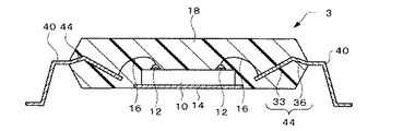
図9に示す例では、半導体装置3のインナーリード44は、半導体装置の外側に向かって上方に傾斜する傾斜部33と、半導体装置の外側に向かって下方に傾斜する第2の傾斜部36とによって形成されてなる。その他の構成については、上記実施の形態で説明した内容を適用することができる。また、図9に示す半導体装置の製造方法は、インナーリード44を屈曲させる点を除き、上記実施の形態で説明した事項を適用することができる。なお、第2の傾斜部36は、インナーリード44を、ダイパッド14のダウンセット方向とは反対の方向に屈曲させることで形成してもよい。また、傾斜部33と第2の傾斜部36とを有するインナーリード44を、治具等を用いて一体的に成型してもよい。
【0056】
なお、本発明を適用した半導体装置のインナーリードの形態は上述の内容に限られない。すなわち、外側に向かって上方に傾斜する傾斜部のみでインナーリードを形成してもよく、傾斜部と傾斜部から水平方向に延びる先端部とでインナーリードを形成してもよい。また、傾斜部の外側には、外側に向かって下方に傾斜する第2の傾斜部、あるいは、アウターリード40から延設されて水平方向に延びる部分のいずれかが形成されてもよく、その両方が形成されてもよい。
【0057】
本発明は、上述した実施の形態に限定されるものではなく、種々の変形が可能である。例えば、本発明は、実施の形態で説明した構成と実質的に同一の構成(例えば、機能、方法及び結果が同一の構成、あるいは目的及び結果が同一の構成)を含む。また、本発明は、実施の形態で説明した構成の本質的でない部分を置き換えた構成を含む。また、本発明は、実施の形態で説明した構成と同一の作用効果を奏する構成又は同一の目的を達成することができる構成を含む。また、本発明は、実施の形態で説明した構成に公知技術を付加した構成を含む。
【図面の簡単な説明】
【図1】図1は、本発明を適用した実施の形態に係る半導体装置を示す図である。
【図2】図2は、本発明を適用した実施の形態に係る半導体装置の製造方法を示す図である。
【図3】図3は、本発明を適用した実施の形態に係る半導体装置の製造方法を示す図である。
【図4】図4は、本発明を適用した実施の形態に係る半導体装置が実装された回路基板を示す図である。
【図5】図5は、本発明を適用した実施の形態に係る半導体装置を有する電子機器を示す図である。
【図6】図6は、本発明を適用した実施の形態に係る半導体装置を有する電子機器を示す図である。
【図7】図7は、本発明を適用した実施の形態に係る半導体装置の変形例を示す図である。
【図8】図8(A)及び図8(B)は、本発明を適用した実施の形態に係る半導体装置の変形例の製造方法を示す図である。
【図9】図9は、本発明を適用した実施の形態に係る半導体装置の変形例を示す図である。
【符号の説明】
10 半導体チップ、 12 電極、 14 ダイパッド、 16 ワイヤ、 18 封止部、 30 インナーリード、 32 傾斜部、 34 先端部、 38 水平方向に延びる部分、 40 アウターリード[0001]
TECHNICAL FIELD OF THE INVENTION
The present invention relates to a semiconductor device and a method for manufacturing the same, a circuit board, and an electronic device.
[0002]
BACKGROUND OF THE INVENTION
Conventionally, in a semiconductor device, it has been known that an electrode of a semiconductor chip and an inner lead are electrically connected by a wire. In this case, it is necessary to bring the wire into contact with only the intended inner lead and to prevent short-circuit with other inner leads.
[0003]
An object of the present invention is to provide a highly reliable semiconductor device in which a short circuit between a bonding wire and an inner lead hardly occurs, a manufacturing method thereof, a circuit board, and an electronic device.
[0004]
[Means for Solving the Problems]
(1) The semiconductor device according to the present invention comprises:
An inner lead having an inclined portion inclined upward toward the outside,
Die pad,
A semiconductor chip having a plurality of electrodes bonded to the die pad,
A wire for electrically connecting the inner lead and the electrode,
A sealing portion for sealing the inner lead and the semiconductor chip and the wire,
An outer lead extending outside the sealing portion,
including.
[0005]
According to the present invention, the position of the tip of the inner lead is reduced. This makes it possible to provide a highly reliable semiconductor device in which the wires connecting the electrodes of the semiconductor chip and the inner leads are less likely to contact inner leads other than the intended inner leads.
[0006]
(2) In this semiconductor device,
The wire may be bonded to the inclined portion.
[0007]
(3) In this semiconductor device,
The inner lead may further include a tip portion extending horizontally from the inclined portion.
[0008]
(4) In this semiconductor device,
The wire may be bonded to the tip.
[0009]
(5) In this semiconductor device,
The inner lead may further include a second inclined portion that is inclined outward and downward below the inclined portion.
[0010]
(6) In this semiconductor device,
The inner lead may further include a portion extending from the outer lead and extending in a horizontal direction.
[0011]
(7) In this semiconductor device,
A bonding position between the wire and the inner lead may be lower than the electrode.
[0012]
(8) In this semiconductor device,
A surface of the die pad opposite to a side on which the semiconductor chip is mounted may be exposed from the sealing portion.
[0013]
(9) The above-described semiconductor device is mounted on a circuit board according to the present invention.
[0014]
(10) An electronic apparatus according to the present invention includes the above semiconductor device.
[0015]
(11) The method for manufacturing a semiconductor device according to the present invention includes:
Bending the inner lead of the lead frame to form an inclined portion inclined upward toward the outside,
Bonding a semiconductor chip having a plurality of electrodes to a die pad of the lead frame,
Electrically connecting the inner lead and the electrode by a wire; and
Sealing the inner leads, the semiconductor chip, and the wires.
[0016]
According to the present invention, the position of the tip of the inner lead is reduced. This makes it difficult for the wire connecting the electrode of the semiconductor chip and the inner lead to contact the inner lead other than the intended inner lead. Therefore, a highly reliable semiconductor device can be manufactured.
[0017]
(12) In this method of manufacturing a semiconductor device,
The wire may be bonded to the inclined portion.
[0018]
(13) In this method of manufacturing a semiconductor device,
The method may further include bending the inner lead to form a tip portion extending horizontally from the inclined portion on the inner lead.
[0019]
(14) In this method of manufacturing a semiconductor device,
The wire may be bonded to the tip.
[0020]
(15) In this method of manufacturing a semiconductor device,
The method may further include bending the inner lead to form a second inclined portion that is inclined outward and downward below the inclined portion of the inner lead.
[0021]
(16) In this method of manufacturing a semiconductor device,
The method may further include forming a portion extending from the outer lead of the lead frame and extending in the horizontal direction on the inner lead.
[0022]
(17) In this method of manufacturing a semiconductor device,
A bonding position between the wire and the inner lead may be lower than the electrode.
[0023]
(18) In this method of manufacturing a semiconductor device,
The method may further include exposing a surface of the die pad opposite to a side on which the semiconductor chip is mounted from a sealing portion.
[0024]
BEST MODE FOR CARRYING OUT THE INVENTION
Hereinafter, embodiments of the present invention will be described with reference to the drawings. However, the present invention is not limited to the following embodiments.
[0025]
FIG. 1 is a sectional view of a semiconductor device according to an embodiment to which the present invention is applied. The semiconductor device according to the present embodiment has a
[0026]
A plurality of
[0027]
On the active surface of the
[0028]
The
[0029]
The semiconductor device according to the present embodiment has a plurality of leads 20. The
[0030]
The
[0031]
The semiconductor device according to the present embodiment has
[0032]
The semiconductor device according to the present embodiment has a sealing
[0033]
The semiconductor device according to the present embodiment has outer leads 40 extending outside sealing
[0034]
The semiconductor device according to the present embodiment is configured as described above, and a manufacturing method thereof will be described below.
[0035]
First, a
[0036]
The
[0037]
The
[0038]
The
[0039]
The
[0040]
The outer leads 40 extend from the
[0041]
Next, the
[0042]
The step of bending the inner leads 30 may be performed before or after the step of downsetting the
[0043]
Next, the
[0044]
Next, the inner leads 30 and the
[0045]
Next, a molding step is performed. Specifically, as shown in FIG. 3, the
[0046]
Next, a first trimming step is performed. That is, the
[0047]
Then, an electrolytic plating step is performed. That is, a metal film such as a brazing material (for example, solder) or tin is formed on a portion of the
[0048]
Next, a second trimming step is performed. That is, the
[0049]
Then, if necessary, the semiconductor device 1 can be manufactured through a marking step, an inspection step, and the like.
[0050]
The
[0051]
FIG. 4 shows a
[0052]
(Modification)
7 to 9 are cross-sectional views of a semiconductor device according to a modification of the embodiment to which the present invention is applied.
[0053]
In the example shown in FIG. 7, the
[0054]
The method described in the above embodiment can be applied to the method of manufacturing the semiconductor device shown in FIG. 7 except that the
[0055]
In the example shown in FIG. 9, the
[0056]
The form of the inner lead of the semiconductor device to which the present invention is applied is not limited to the above. That is, the inner lead may be formed only by the inclined portion that is inclined upward toward the outside, or the inner lead may be formed by the inclined portion and the tip portion extending in the horizontal direction from the inclined portion. Further, on the outside of the inclined portion, either a second inclined portion inclined downward toward the outside or a portion extending from the
[0057]
The present invention is not limited to the embodiments described above, and various modifications are possible. For example, the invention includes configurations substantially the same as the configurations described in the embodiments (for example, a configuration having the same function, method, and result, or a configuration having the same object and result). Further, the invention includes a configuration in which a non-essential part of the configuration described in the embodiment is replaced. Further, the invention includes a configuration having the same operation and effect as the configuration described in the embodiment, or a configuration capable of achieving the same object. Further, the invention includes a configuration in which a known technique is added to the configuration described in the embodiment.
[Brief description of the drawings]
FIG. 1 is a diagram showing a semiconductor device according to an embodiment to which the present invention is applied.
FIG. 2 is a diagram illustrating a method of manufacturing a semiconductor device according to an embodiment to which the present invention is applied.
FIG. 3 is a diagram showing a method of manufacturing a semiconductor device according to an embodiment to which the present invention is applied.
FIG. 4 is a diagram showing a circuit board on which a semiconductor device according to an embodiment to which the present invention is applied is mounted;
FIG. 5 is a diagram illustrating an electronic apparatus including a semiconductor device according to an embodiment to which the present invention is applied;
FIG. 6 is a diagram illustrating an electronic apparatus including a semiconductor device according to an embodiment to which the present invention is applied;
FIG. 7 is a diagram showing a modification of the semiconductor device according to the embodiment to which the present invention is applied;
FIGS. 8A and 8B are views showing a method of manufacturing a modification of the semiconductor device according to the embodiment to which the present invention is applied;
FIG. 9 is a diagram showing a modification of the semiconductor device according to the embodiment to which the present invention is applied;
[Explanation of symbols]
Claims (18)
ダイパッドと、
前記ダイパッドにボンディングされてなる、複数の電極を有する半導体チップと、
前記インナーリードと前記電極とを電気的に接続するワイヤと、
前記インナーリード及び前記半導体チップ並びに前記ワイヤを封止する封止部と、
前記封止部の外側に延びるアウターリードと、
を含む半導体装置。An inner lead having an inclined portion inclined upward toward the outside,
Die pad,
A semiconductor chip having a plurality of electrodes bonded to the die pad,
A wire for electrically connecting the inner lead and the electrode,
A sealing portion for sealing the inner lead and the semiconductor chip and the wire,
An outer lead extending outside the sealing portion,
Semiconductor device including:
前記ワイヤは前記傾斜部にボンディングされてなる半導体装置。The semiconductor device according to claim 1,
A semiconductor device in which the wire is bonded to the inclined portion.
前記インナーリードは、前記傾斜部から水平方向に延びる先端部をさらに有する半導体装置。The semiconductor device according to claim 1,
The semiconductor device, wherein the inner lead further has a tip portion extending horizontally from the inclined portion.
前記ワイヤは前記先端部にボンディングされてなる半導体装置。The semiconductor device according to claim 3,
A semiconductor device in which the wire is bonded to the tip.
前記インナーリードは、前記傾斜部の外側に、外側に向かって下方に傾斜する第2の傾斜部をさらに有する半導体装置。The semiconductor device according to claim 1, wherein
The semiconductor device, wherein the inner lead further includes a second inclined portion that is inclined downward toward the outside outside the inclined portion.
前記インナーリードは、前記アウターリードから延設されて水平方向に延びる部分をさらに有する半導体装置。The semiconductor device according to any one of claims 1 to 5,
The semiconductor device, wherein the inner lead further includes a portion extending from the outer lead and extending in a horizontal direction.
前記ワイヤと前記インナーリードとのボンディング位置は、前記電極よりも低い半導体装置。7. The semiconductor device according to claim 1, wherein:
A semiconductor device wherein a bonding position between the wire and the inner lead is lower than the electrode.
前記ダイパッドにおける前記半導体チップが搭載された側とは反対側の面が、前記封止部から露出してなる半導体装置。The semiconductor device according to any one of claims 1 to 7,
A semiconductor device in which a surface of the die pad opposite to a side on which the semiconductor chip is mounted is exposed from the sealing portion.
前記リードフレームのダイパッドに複数の電極を有する半導体チップをボンディングすること、
前記インナーリードと前記電極とをワイヤによって電気的に接続すること、及び、
前記インナーリード及び前記半導体チップ並びに前記ワイヤを封止することを含む半導体装置の製造方法。Bending the inner lead of the lead frame to form an inclined portion inclined upward toward the outside,
Bonding a semiconductor chip having a plurality of electrodes to a die pad of the lead frame,
Electrically connecting the inner lead and the electrode by a wire; and
A method for manufacturing a semiconductor device, comprising sealing the inner lead, the semiconductor chip, and the wire.
前記ワイヤを前記傾斜部にボンディングする半導体装置の製造方法。The method for manufacturing a semiconductor device according to claim 11,
A method for manufacturing a semiconductor device, wherein the wire is bonded to the inclined portion.
前記インナーリードを屈曲させて、前記インナーリードに前記傾斜部から水平方向に延びる先端部を形成することをさらに含む半導体装置の製造方法。The method for manufacturing a semiconductor device according to claim 11,
A method of manufacturing a semiconductor device, further comprising bending the inner lead to form a tip portion extending horizontally from the inclined portion on the inner lead.
前記ワイヤを前記先端部にボンディングする半導体装置の製造方法。The method for manufacturing a semiconductor device according to claim 13,
A method of manufacturing a semiconductor device, wherein the wire is bonded to the tip.
前記インナーリードを屈曲させて、前記インナーリードの前記傾斜部の外側に、外側に向かって下方に傾斜する第2の傾斜部を形成することをさらに含む半導体装置の製造方法。The method for manufacturing a semiconductor device according to any one of claims 11 to 14,
A method of manufacturing a semiconductor device, further comprising bending the inner lead to form a second inclined portion that is inclined downward and outward outside the inclined portion of the inner lead.
前記インナーリードに、前記リードフレームのアウターリードから延設されて水平方向に延びる部分を形成することをさらに含む半導体装置の製造方法。The method for manufacturing a semiconductor device according to any one of claims 11 to 15,
The method of manufacturing a semiconductor device, further comprising forming a portion extending from the outer lead of the lead frame and extending in the horizontal direction on the inner lead.
前記ワイヤと前記インナーリードとのボンディング位置を、前記電極よりも低くする半導体装置の製造方法。The method for manufacturing a semiconductor device according to any one of claims 11 to 16,
A method of manufacturing a semiconductor device, wherein a bonding position between the wire and the inner lead is lower than the electrode.
前記ダイパッドにおける前記半導体チップが搭載された側とは反対側の面を、封止部から露出させることをさらに含む半導体装置の製造方法。The method of manufacturing a semiconductor device according to claim 11,
A method for manufacturing a semiconductor device, further comprising exposing a surface of the die pad opposite to a side on which the semiconductor chip is mounted from a sealing portion.
Priority Applications (2)
| Application Number | Priority Date | Filing Date | Title |
|---|---|---|---|
| JP2002281082A JP2004119699A (en) | 2002-09-26 | 2002-09-26 | Semiconductor device and its manufacturing method, circuit board, and electronic equipment |
| US10/664,585 US20040119146A1 (en) | 2002-09-26 | 2003-09-17 | Semiconductor device and method of manufacturing the same, circuit board, and electronic instrument |
Applications Claiming Priority (1)
| Application Number | Priority Date | Filing Date | Title |
|---|---|---|---|
| JP2002281082A JP2004119699A (en) | 2002-09-26 | 2002-09-26 | Semiconductor device and its manufacturing method, circuit board, and electronic equipment |
Publications (1)
| Publication Number | Publication Date |
|---|---|
| JP2004119699A true JP2004119699A (en) | 2004-04-15 |
Family
ID=32275628
Family Applications (1)
| Application Number | Title | Priority Date | Filing Date |
|---|---|---|---|
| JP2002281082A Withdrawn JP2004119699A (en) | 2002-09-26 | 2002-09-26 | Semiconductor device and its manufacturing method, circuit board, and electronic equipment |
Country Status (2)
| Country | Link |
|---|---|
| US (1) | US20040119146A1 (en) |
| JP (1) | JP2004119699A (en) |
Cited By (1)
| Publication number | Priority date | Publication date | Assignee | Title |
|---|---|---|---|---|
| JP2023108665A (en) * | 2022-01-26 | 2023-08-07 | エイブリック株式会社 | Lead frame and semiconductor device using it |
Families Citing this family (2)
| Publication number | Priority date | Publication date | Assignee | Title |
|---|---|---|---|---|
| JPWO2005114730A1 (en) * | 2004-05-20 | 2008-03-27 | スパンション エルエルシー | Semiconductor device manufacturing method and semiconductor device |
| JP2006073904A (en) * | 2004-09-06 | 2006-03-16 | Matsushita Electric Ind Co Ltd | Semiconductor device, lead frame, and manufacturing method thereof |
Family Cites Families (10)
| Publication number | Priority date | Publication date | Assignee | Title |
|---|---|---|---|---|
| JPH05144992A (en) * | 1991-11-18 | 1993-06-11 | Mitsubishi Electric Corp | Semiconductor device, manufacturing method thereof, lead frame used for manufacturing the same, and manufacturing method thereof |
| US5389739A (en) * | 1992-12-15 | 1995-02-14 | Hewlett-Packard Company | Electronic device packaging assembly |
| JPH10242360A (en) * | 1997-02-25 | 1998-09-11 | Oki Electric Ind Co Ltd | Semiconductor device |
| WO1998042022A1 (en) * | 1997-03-18 | 1998-09-24 | Seiko Epson Corporation | Semiconductor device and method of manufacturing same |
| US6157074A (en) * | 1997-07-16 | 2000-12-05 | Hyundai Electronics Industries Co., Ltd. | Lead frame adapted for variable sized devices, semiconductor package with such lead frame and method for using same |
| US6143981A (en) * | 1998-06-24 | 2000-11-07 | Amkor Technology, Inc. | Plastic integrated circuit package and method and leadframe for making the package |
| US6831352B1 (en) * | 1998-10-22 | 2004-12-14 | Azimuth Industrial Company, Inc. | Semiconductor package for high frequency performance |
| US6291881B1 (en) * | 1999-03-04 | 2001-09-18 | United Microelectronics Corp. | Dual silicon chip package |
| US6316727B1 (en) * | 1999-10-07 | 2001-11-13 | United Microelectronics Corp. | Multi-chip semiconductor package |
| US6818973B1 (en) * | 2002-09-09 | 2004-11-16 | Amkor Technology, Inc. | Exposed lead QFP package fabricated through the use of a partial saw process |
-
2002
- 2002-09-26 JP JP2002281082A patent/JP2004119699A/en not_active Withdrawn
-
2003
- 2003-09-17 US US10/664,585 patent/US20040119146A1/en not_active Abandoned
Cited By (2)
| Publication number | Priority date | Publication date | Assignee | Title |
|---|---|---|---|---|
| JP2023108665A (en) * | 2022-01-26 | 2023-08-07 | エイブリック株式会社 | Lead frame and semiconductor device using it |
| JP7825430B2 (en) | 2022-01-26 | 2026-03-06 | エイブリック株式会社 | Lead frame and semiconductor device using the same |
Also Published As
| Publication number | Publication date |
|---|---|
| US20040119146A1 (en) | 2004-06-24 |
Similar Documents
| Publication | Publication Date | Title |
|---|---|---|
| US7285855B2 (en) | Packaged device and method of forming same | |
| CN102034802B (en) | STRUCTURE AND METHOD FOR STANDARD CHIP SCALE PACKAGING | |
| JP5341337B2 (en) | Semiconductor device and manufacturing method thereof | |
| CN101421833B (en) | Method for packaging integrated circuit die | |
| JP2004526333A (en) | Carrier with metal protrusions for semiconductor die packages | |
| KR20080108908A (en) | Semiconductor device, manufacturing method thereof and semiconductor device product | |
| JP3664045B2 (en) | Manufacturing method of semiconductor device | |
| CN101877339A (en) | Lead frame | |
| CN102456648B (en) | Manufacturing method of package substrate | |
| JP2019176034A (en) | Semiconductor device and method for manufacturing semiconductor device | |
| JP2915282B2 (en) | Plastic molded integrated circuit package | |
| JP2002026044A (en) | Semiconductor device and its manufacturing method, circuit board, and electronic equipment | |
| CN102456649A (en) | Packaging substrate and its manufacturing method | |
| JPH11163024A (en) | Semiconductor device, lead frame for assembling the same, and method of manufacturing semiconductor device | |
| US7875964B2 (en) | Multi-chip semiconductor connector and method | |
| CN100508111C (en) | Packaging device and forming method thereof | |
| JP2003197663A (en) | Semiconductor device and its manufacturing method, circuit board, and electronic equipment | |
| JP2004119699A (en) | Semiconductor device and its manufacturing method, circuit board, and electronic equipment | |
| JP2002190544A (en) | Wiring board, semiconductor device, and method of manufacturing the same | |
| JPH0917910A (en) | Semiconductor device, manufacturing method thereof, inspection method, and mounting substrate | |
| JPH0812895B2 (en) | Semiconductor device mounted pin grid array package substrate | |
| CN107275308A (en) | Semiconductor encapsulation device, semiconductor lead frame and its rib cutting method | |
| JP2001257304A (en) | Semiconductor device and mounting method thereof | |
| JP2001230345A (en) | Semiconductor device, manufacturing method thereof, and lead frame used for manufacturing the same | |
| JP2004119700A (en) | Semiconductor device and its manufacturing method, circuit board, and electronic equipment |
Legal Events
| Date | Code | Title | Description |
|---|---|---|---|
| A621 | Written request for application examination |
Free format text: JAPANESE INTERMEDIATE CODE: A621 Effective date: 20050819 |
|
| RD04 | Notification of resignation of power of attorney |
Free format text: JAPANESE INTERMEDIATE CODE: A7424 Effective date: 20051220 |
|
| A977 | Report on retrieval |
Free format text: JAPANESE INTERMEDIATE CODE: A971007 Effective date: 20060222 |
|
| A131 | Notification of reasons for refusal |
Free format text: JAPANESE INTERMEDIATE CODE: A131 Effective date: 20061004 |
|
| A521 | Request for written amendment filed |
Free format text: JAPANESE INTERMEDIATE CODE: A523 Effective date: 20061201 |
|
| A131 | Notification of reasons for refusal |
Free format text: JAPANESE INTERMEDIATE CODE: A131 Effective date: 20070117 |
|
| A521 | Request for written amendment filed |
Free format text: JAPANESE INTERMEDIATE CODE: A523 Effective date: 20070315 |
|
| A131 | Notification of reasons for refusal |
Free format text: JAPANESE INTERMEDIATE CODE: A131 Effective date: 20081105 |
|
| A761 | Written withdrawal of application |
Free format text: JAPANESE INTERMEDIATE CODE: A761 Effective date: 20081226 |