CN1602555A - Chip lead frame of radiating element, radiating element and manufacturing method thereof - Google Patents
Chip lead frame of radiating element, radiating element and manufacturing method thereof Download PDFInfo
- Publication number
- CN1602555A CN1602555A CN02811663.1A CN02811663A CN1602555A CN 1602555 A CN1602555 A CN 1602555A CN 02811663 A CN02811663 A CN 02811663A CN 1602555 A CN1602555 A CN 1602555A
- Authority
- CN
- China
- Prior art keywords
- chip
- lead frame
- radiation
- thermal connection
- housing
- Prior art date
- Legal status (The legal status is an assumption and is not a legal conclusion. Google has not performed a legal analysis and makes no representation as to the accuracy of the status listed.)
- Granted
Links
Images


Classifications
-
- H—ELECTRICITY
- H10—SEMICONDUCTOR DEVICES; ELECTRIC SOLID-STATE DEVICES NOT OTHERWISE PROVIDED FOR
- H10H—INORGANIC LIGHT-EMITTING SEMICONDUCTOR DEVICES HAVING POTENTIAL BARRIERS
- H10H20/00—Individual inorganic light-emitting semiconductor devices having potential barriers, e.g. light-emitting diodes [LED]
- H10H20/80—Constructional details
- H10H20/85—Packages
- H10H20/857—Interconnections, e.g. lead-frames, bond wires or solder balls
-
- H—ELECTRICITY
- H10—SEMICONDUCTOR DEVICES; ELECTRIC SOLID-STATE DEVICES NOT OTHERWISE PROVIDED FOR
- H10H—INORGANIC LIGHT-EMITTING SEMICONDUCTOR DEVICES HAVING POTENTIAL BARRIERS
- H10H20/00—Individual inorganic light-emitting semiconductor devices having potential barriers, e.g. light-emitting diodes [LED]
- H10H20/80—Constructional details
- H10H20/85—Packages
- H10H20/858—Means for heat extraction or cooling
- H10H20/8582—Means for heat extraction or cooling characterised by their shape
-
- H—ELECTRICITY
- H10—SEMICONDUCTOR DEVICES; ELECTRIC SOLID-STATE DEVICES NOT OTHERWISE PROVIDED FOR
- H10H—INORGANIC LIGHT-EMITTING SEMICONDUCTOR DEVICES HAVING POTENTIAL BARRIERS
- H10H20/00—Individual inorganic light-emitting semiconductor devices having potential barriers, e.g. light-emitting diodes [LED]
- H10H20/80—Constructional details
- H10H20/85—Packages
- H10H20/8506—Containers
-
- H—ELECTRICITY
- H10—SEMICONDUCTOR DEVICES; ELECTRIC SOLID-STATE DEVICES NOT OTHERWISE PROVIDED FOR
- H10H—INORGANIC LIGHT-EMITTING SEMICONDUCTOR DEVICES HAVING POTENTIAL BARRIERS
- H10H20/00—Individual inorganic light-emitting semiconductor devices having potential barriers, e.g. light-emitting diodes [LED]
- H10H20/80—Constructional details
- H10H20/85—Packages
- H10H20/855—Optical field-shaping means, e.g. lenses
- H10H20/856—Reflecting means
-
- H—ELECTRICITY
- H10—SEMICONDUCTOR DEVICES; ELECTRIC SOLID-STATE DEVICES NOT OTHERWISE PROVIDED FOR
- H10W—GENERIC PACKAGES, INTERCONNECTIONS, CONNECTORS OR OTHER CONSTRUCTIONAL DETAILS OF DEVICES COVERED BY CLASS H10
- H10W72/00—Interconnections or connectors in packages
- H10W72/851—Dispositions of multiple connectors or interconnections
- H10W72/874—On different surfaces
- H10W72/884—Die-attach connectors and bond wires
-
- H—ELECTRICITY
- H10—SEMICONDUCTOR DEVICES; ELECTRIC SOLID-STATE DEVICES NOT OTHERWISE PROVIDED FOR
- H10W—GENERIC PACKAGES, INTERCONNECTIONS, CONNECTORS OR OTHER CONSTRUCTIONAL DETAILS OF DEVICES COVERED BY CLASS H10
- H10W90/00—Package configurations
- H10W90/701—Package configurations characterised by the relative positions of pads or connectors relative to package parts
- H10W90/731—Package configurations characterised by the relative positions of pads or connectors relative to package parts of die-attach connectors
- H10W90/736—Package configurations characterised by the relative positions of pads or connectors relative to package parts of die-attach connectors between a chip and a stacked lead frame, conducting package substrate or heat sink
-
- H—ELECTRICITY
- H10—SEMICONDUCTOR DEVICES; ELECTRIC SOLID-STATE DEVICES NOT OTHERWISE PROVIDED FOR
- H10W—GENERIC PACKAGES, INTERCONNECTIONS, CONNECTORS OR OTHER CONSTRUCTIONAL DETAILS OF DEVICES COVERED BY CLASS H10
- H10W90/00—Package configurations
- H10W90/701—Package configurations characterised by the relative positions of pads or connectors relative to package parts
- H10W90/751—Package configurations characterised by the relative positions of pads or connectors relative to package parts of bond wires
- H10W90/756—Package configurations characterised by the relative positions of pads or connectors relative to package parts of bond wires between a chip and a stacked lead frame, conducting package substrate or heat sink
Landscapes
- Led Device Packages (AREA)
- Led Devices (AREA)
- Cooling Or The Like Of Electrical Apparatus (AREA)
Abstract
Description
本发明涉及权利要求1前序部分所述的一种芯片引线架、权利要求14前序部分所述的一种外壳、权利要求23前序部分所述的一种辐射元件以及权利要求33前序部分所述的该元件的一种制造方法。The invention relates to a chip lead frame according to the preamble of
例如从DE 196 36 454已知发出辐射的半导体元件的芯片引线架。该处描述的半导体元件具有一个埋入了芯片引线架的外壳基体以及一个发出辐射的半导体本体,该半导体本体安装在该芯片引线架上。该芯片引线架和外壳基体同时设计成产生辐射的反射器。For example from DE 196 36 454 a chip lead frame of a radiation-emitting semiconductor element is known. The semiconductor component described here has a housing base body in which the chip lead frame is embedded, and a radiation-emitting semiconductor body, which is mounted on the chip lead frame. The chip lead frame and the housing base body are simultaneously designed as radiation-generating reflectors.
此外,从外壳基体伸出的芯片引线架的部分区域作为外部电连接条构成,而外壳则设计成适合于表面安装元件。为了达到尤其是在大功率半导体元件时产生的损耗热的良好的散热,反射器的一部分可作为热连接从外壳基体引出。Furthermore, parts of the chip lead frame protruding from the base body of the housing are formed as external electrical connection bars, while the housing is designed for surface-mounted components. In order to achieve good dissipation of the heat dissipated, especially in the case of high-power semiconductor components, a part of the reflector can be led out of the housing base as a thermal connection.
对高发光效率和相应大的损耗功率的元件来说,希望或需要更有效的散热。For components with high luminous efficacy and correspondingly large power losses, more efficient heat dissipation is desired or required.
本发明的目的是对辐射元件提出一种改进的散热,从而可在元件内产生高发光效率。此外,本发明的目的是提出这种元件的制造方法。The object of the present invention is to propose an improved heat dissipation of the radiating element so that a high luminous efficiency can be produced within the element. Furthermore, the object of the invention is to propose a method for the manufacture of such an element.
这个目的是通过权利要求1的一个芯片引线架、权利要求14的一个外壳、权利要求23的一个辐射元件或权利要求33的一种方法来实现的。本发明的诸多有利改进方案可从各项从属权利要求的内容得知。This object is achieved by a chip lead frame according to
根据本发明,辐射元件尤指发光二极管的芯片引线架具有至少一个芯片安装区、至少一个引线连接区和至少一个例如用来把元件安装并连接到一块印刷电路板上的外部连接条,并设置了一个支承部分,该支承部分具有引线连接区和电连接条并在其中嵌入一个与芯片引线架隔开的单独制造的热连接部分,后者设有芯片安装区。具有这种芯片引线架的元件在运行中产生的损耗热主要通过这个热连接部分来散热。这个热连接部分最好与支承部分进行电连接,并同时作为芯片的电连接用。According to the invention, the chip lead frame of the radiating element, especially a light-emitting diode, has at least one chip mounting area, at least one lead connection area and at least one external connection bar, for example, for mounting and connecting the component to a printed circuit board, and is arranged A support portion is provided having lead connection areas and electrical connection bars and embedded therein is a separately fabricated thermal connection portion spaced from the chip lead frame, the latter being provided with the chip mounting area. The dissipated heat generated during operation of components with such a chip lead frame is mainly dissipated through this thermal connection portion. This thermal connection is preferably electrically connected to the support and at the same time serves as an electrical connection to the chip.
与芯片引线架隔开单独制造的热连接部分具有这样的优点,即在大量损耗热的吸收和散发方面可达到最佳化而比整体的芯片引线架好得多。所以在这种热连接部分时,厚度、导热率、热膨胀系数和热连接面都可达到最佳化而几乎与对芯片引线架的要求无关。特别是,这种热连接部分可达到高的热容量,所以该热连接部分构成一个有效的散热源。一个大的热连接面可减小热阻,并由此改善导热和把热散发到周围。A separately manufactured thermal connection from the chip lead frame has the advantage that absorption and dissipation of the bulky heat loss can be optimized much better than an integral chip lead frame. Therefore, in this thermal connection part, the thickness, thermal conductivity, thermal expansion coefficient and thermal connection surface can all be optimized and have almost nothing to do with the requirements of the chip lead frame. In particular, such a thermal connection can achieve a high heat capacity, so that the thermal connection constitutes an effective heat dissipation source. A large thermal connection area reduces thermal resistance and thus improves heat conduction and heat dissipation to the surroundings.
在本发明的一个优选方案中,支承部分具有一个例如夹箍或夹环形式的嵌入孔,该热连接部分嵌入其中。这里可理解成将热连接元件嵌入芯片引线架的嵌入孔中,且其周边与芯片引线架连接。In a preferred embodiment of the invention, the support part has an insertion hole, for example in the form of a clip or a clamping ring, into which the thermal connection part is inserted. It can be understood here that the thermal connection element is embedded in the embedding hole of the chip lead frame, and its periphery is connected with the chip lead frame.
为此,这个热连接部分例如可卡入该支承部分中和/或与它挤紧连接或铆接。根据本发明,最好在热连接部分和支承部分之间构成挤紧连接,这种挤紧连接的特点是具有高的机械强度和优良的导电率。挤紧连接例如可这样构成:支承部分和热连接部分例如通过把该连接部分嵌入支承部分的一个嵌入孔中来实现该支承部分和热连接部分的相互定位,然后热连接部分这样变形,即在支承部分中形成连接部分的机械的固定位置。可用锤或冲头之类的工具来产生变形。For this purpose, the thermal connection part can be snapped into the bearing part and/or squeezed or riveted to it, for example. According to the invention, preferably a squeeze connection is formed between the thermal connection part and the support part, which is characterized by high mechanical strength and good electrical conductivity. Squeeze connection can for example be constituted like this: support part and thermal connection part realize mutual positioning of this support part and thermal connection part, for example by inserting this connection part in an insertion hole of support part, and then thermal connection part is deformed like this, promptly in The mechanically fixed position of the connection part is formed in the support part. Tools such as hammers or punches can be used to create deformation.
连接部分最好这样成形,即它可按铆钉的方式与支承部分连接。在一定情况下,连接部分的单个接片或撑条的变形也能满足在连接部分和支承部分之间形成足够强度的挤紧连接。The connection part is preferably formed in such a way that it can be connected to the support part in the manner of a rivet. Under certain circumstances, the deformation of individual webs or struts of the connecting part is also sufficient to form a sufficiently strong squeeze connection between the connecting part and the support part.
在本发明的范围内可在连接部分和支承部分之间建立附加的或另外的其他连接例如钎焊或熔焊连接也是适合的。此外,连接部分还与支承部分进行粘接。It is also suitable within the scope of the invention to produce additional or further other connections, for example soldered or welded connections, between the connection part and the support part. In addition, the connection part is also glued to the support part.
半导体元件的这样构成的一个机械稳定的支架具有这样的优点,即用相当少的技术费用就可把它制造出来。A mechanically stable carrier formed in this way for the semiconductor element has the advantage that it can be produced with relatively little technical effort.
热连接部分最好具有一个反射槽。在由此构成的元件时,这种热连接部分可改善元件的辐射效率和射束聚束。在本发明的这个方案时,最好用一种金属的热连接部分,因为金属表面以其很小的吸收损失和很强的定向反射而很适合作反射器表面。The thermal connection preferably has a reflective groove. In the case of components thus constructed, such a thermal connection improves the radiation efficiency and beam focusing of the component. In this version of the invention, it is preferable to use a metallic thermal connection, since metal surfaces are well suited as reflector surfaces with their low absorption losses and strong directional reflections.
为了提高机械稳定性,尤其是对下面尚待详细说明的外壳或元件来说,热连接部分的反射槽的高度最好这样选定,使它不超过一个设置在安装区的芯片的两倍高度。In order to improve mechanical stability, especially for housings or components to be described in detail below, the height of the reflection groove of the thermal connection part is preferably selected so that it does not exceed twice the height of a chip arranged in the mounting area .
适合作热连接部分的材料是具有高导热率的金属,特别是铜或铝或它们的合金。此外,其他优选的材料有钼、铁、镍和钨以及镍铁合金和铜钨合金,它们的热膨胀系数与半导体材料例如砷化镓(GaAs)、氮化镓(GaN)和以它们为基础的材料的热膨胀系数很匹配。其他适合作热连接部分的材料为陶瓷和硅之类的半导体。热连接部分也可是多层的,例如构成金属陶瓷复合系统。Suitable materials for the thermal connection are metals with high thermal conductivity, especially copper or aluminum or their alloys. In addition, other preferred materials are molybdenum, iron, nickel and tungsten as well as nickel-iron alloys and copper-tungsten alloys, which have the same thermal expansion coefficient as semiconductor materials such as gallium arsenide (GaAs), gallium nitride (GaN) and materials based on them. The thermal expansion coefficients are well matched. Other suitable materials for the thermal connection are ceramics and semiconductors such as silicon. The thermal connection can also be multilayered, for example to form a metal-ceramic composite system.
热连接部分的芯片安装表面最好进行调质处理,调质处理可改善芯片安装的表面性能(键合性能)。这种调质处理例如可包括涂覆一层银或金。The chip mounting surface of the thermal connection part is preferably subjected to quenching and tempering treatment, which can improve the surface performance (bonding performance) of chip mounting. Such tempering may include, for example, a coating of silver or gold.
还有焊接连接条或引线连接区进行表面调质处理例如涂覆一层金、银、锡或锌来改善焊接或键合性能,在很大程度上也是有利的。It is also advantageous to a large extent that the solder connection strip or the lead connection area be subjected to surface conditioning treatment such as coating a layer of gold, silver, tin or zinc to improve soldering or bonding performance.
支承部分最好含铜或软铁并可例如用相应的箔冲压而成。根据本发明,这种支承部分有利于散热,所以对供电功能以及在下面还要详细说明的一种模塑材料的弯曲性能和附着性能都可达到最佳化。The support part preferably contains copper or soft iron and can be stamped, for example, from a corresponding foil. According to the invention, the supporting portion facilitates heat dissipation, so that the power supply function as well as the bending properties and adhesion properties of a molding material which will be described in detail below can be optimized.
这方面例如包括:支承部分在其厚度上可这样制作,即从一卷支承带进行加工、稍为冲压即可弯曲成型。这类加工性能有利于自动化生产和支承带上单个元件的密集布置(很小的间距)。This aspect includes, for example, that the thickness of the supporting part can be produced in such a way that it is processed from a roll of supporting strip, can be bent into shape with a little stamping. Such processability facilitates automated production and the dense arrangement (very small pitches) of the individual elements on the carrier strip.
这样要求的支承部分的很小厚度一般对芯片的足够冷却造成了困难。特别是由于机械稳定性的原因限制了热连接的横截面。本发明通过嵌入热连接部分而消除了这个缺点。The small thickness of the support part required in this way generally creates difficulties for adequate cooling of the chips. In particular, the cross-section of the thermal connection is limited for reasons of mechanical stability. The present invention eliminates this disadvantage by embedding the thermal connection.
根据本发明,为了构成辐射元件的外壳,芯片引线架最好被外壳基体包封。为此,芯片引线架最好埋入一种构成该外壳基体的模塑材料例如注塑或压铸材料中。这样就可用注塑法或压铸法进行经济的外壳制造。模塑材料例如可用环氧树脂或丙烯酸树脂为基础的塑料,但也可用任一种其他适合于这种使用目的的材料。为了散热,热连接部分最好这样埋入:它部分地从外壳基体伸出或构成外壳基体的一部分并由此可从外部进行热连接。According to the invention, in order to form the housing of the radiating element, the chip lead frame is preferably enclosed by the housing base body. For this purpose, the chip lead frame is preferably embedded in a molding material, such as injection molding or die-casting material, which forms the base body of the housing. This allows an economical production of the housing by injection molding or die casting. The molding material may be, for example, epoxy- or acrylic-based plastics, but any other material suitable for the purpose of use may also be used. For heat dissipation, the thermal connection is preferably embedded in such a way that it protrudes partially from the housing base body or forms part of the housing base body and thus can be thermally connected from the outside.
在外壳基体中最好构成一个辐射出射窗口形式的孔口,并将热连接部分这样埋入外壳基体中,使芯片安装区位于辐射出射窗口以内。芯片安装区例如可构成辐射出射窗口的一个界定面。Preferably, an opening in the form of a radiation exit window is formed in the housing base body, and the thermal connection is embedded in the housing base body in such a way that the chip mounting area lies within the radiation exit window. The chip mounting region can form, for example, a delimiting surface of the radiation exit window.
这种外壳形状特别适合于可表面安装的元件,辐射出射窗口对面的一侧或外壳基体的一个侧面构成元件的一个支承面。埋入的热连接部分最好一直延伸到这个支承面,这样,通过该支承面就可同时把损耗热散发到一个冷却体或印制电路板上。热连接部分最好这样设计,使其表面的一部分同时构成支承面或支承面的一部分。This housing shape is particularly suitable for surface-mountable components, the side opposite the radiation exit window or a side of the housing base body forming a support surface for the component. The embedded thermal connection preferably extends as far as this support surface, so that heat losses can simultaneously be dissipated via the support surface to a heat sink or printed circuit board. The thermal connection is preferably designed such that a part of its surface simultaneously forms the bearing surface or a part of the bearing surface.
为了提高辐射效率,外壳基体内的辐射出射窗口可做成圆锥形。这样,它的侧壁就构成了一个反射器。通过这个反射器可使位于芯片安装区的辐射源朝主辐射方向偏转到发射辐射分量的一侧。这样就达到了辐射效率的提高和辐射的聚束改进。In order to improve the radiation efficiency, the radiation exit window in the shell matrix can be made into a conical shape. Thus, its side walls constitute a reflector. The radiation source located in the chip mounting area can be deflected in the direction of the main radiation direction to the side emitting the radiation component by means of this reflector. This achieves an increased radiation efficiency and improved beamforming of the radiation.
反射器最好这样造型,使热连接部分构成反射器的第一区段,在该第一区段上连接一个由辐射出射窗口的侧壁构成的反射器第二区段。反射器的总高度最好小于一个用来安装在芯片装配区上的芯片的四倍高度。这样就可保证高的机械稳定性,并把由于温度变化产生的应力例如焊接过程中产生的应力限制到容许的范围。The reflector is preferably shaped such that the thermal connection forms a first section of the reflector, to which a second section of the reflector formed by the side walls of the radiation exit window adjoins. The overall height of the reflector is preferably less than four times the height of a chip intended to be mounted on the chip mounting area. This ensures high mechanical stability and limits stresses due to temperature changes, for example during welding, to permissible limits.
此外,用本发明的一个芯片引线架或外壳可构成一个具有改善散热的发射辐射元件。这个元件具有一个发出辐射的芯片最好是一个半导体芯片,该芯片布置在热连接部分的芯片安装区上。Furthermore, a chip lead frame or housing according to the invention can be used to construct a radiation-emitting element with improved heat dissipation. This component has a radiation-emitting chip, preferably a semiconductor chip, which is arranged on the chip mounting area of the thermal connection.
该芯片最好至少部分地被一种浇注材料包封。这种实施方案特别适用于具有一个在一个辐射出射窗口中布置了芯片的外壳,其中该辐射出射窗口完全或部分地用上述浇注材料填充。作为浇注材料特别适合用反应性树脂,例如环氧树脂、丙烯酸树脂或硅树脂或它们的混合。在浇注材料中也可添加发光物质,这种发光物质把芯片产生的辐射转换成别的波长范围。这个实施方案特别适用于发射混合色或白色光的元件。The chip is preferably encapsulated at least partially by a potting compound. This embodiment is particularly suitable for housings with a chip arranged in a radiation exit window, wherein the radiation exit window is completely or partially filled with the aforementioned potting compound. Reactive resins such as epoxy resins, acrylic resins or silicone resins or mixtures thereof are particularly suitable as potting compound. Luminescent substances can also be added to the potting compound, which convert the radiation generated by the chip into other wavelength ranges. This embodiment is particularly suitable for elements emitting mixed-color or white light.
为了使外壳、芯片和浇注材料之间的热翘曲保持最小,特别是为了避免浇注保护层的剥落,最好这样选择浇注体积V,使之与芯片的高度H满足下列关系:In order to keep the thermal warpage between housing, chip and potting material to a minimum, and in particular to avoid peeling off of the potting protective layer, it is best to choose the potting volume V so that it satisfies the following relationship with the height H of the chip:
V≤q·HV≤q·H
式中q表示比例系数,其值小于10毫米2,最好为7毫米2。In the formula, q represents a proportionality coefficient, and its value is less than 10 mm 2 , preferably 7 mm 2 .
在本发明的一个优选方案中,芯片引线架分成第一和第二电连接部分,其中热连接部分嵌入第一电连接部分并在第二电连接部分上构成引线连接区。为了供电,一根引线从芯片的接触面引到引线连接区。In a preferred solution of the present invention, the chip lead frame is divided into first and second electrical connection parts, wherein the thermal connection part is embedded in the first electrical connection part and forms a lead connection area on the second electrical connection part. For power supply, a lead is led from the contact surface of the chip to the lead connection area.
本发明元件的制造方法从制造一个支承部分开始,该支承部分例如事先从一条带或箔冲制而成。The method of manufacturing the element according to the invention starts with the manufacture of a support part, which is punched, for example, beforehand from a strip or foil.
在下一个步骤中,将一个单独制作的热连接部分嵌入该支承部分为此设置的一个孔中。然后将芯片安装到热连接部分上,例如通过用一种导电的粘接剂粘接或通过焊接。接着把这样形成的芯片引线架用一种合适的外壳模塑材料进行包封,以构成外壳,例如用一种注塑法或一种压铸法进行。In a next step, a separately produced thermal connection part is inserted into a hole provided for this purpose in the carrier part. The chip is then mounted on the thermal connection, for example by bonding with an electrically conductive adhesive or by soldering. The chip lead frame thus formed is subsequently encapsulated with a suitable housing molding material to form the housing, for example by an injection molding method or an injection molding method.
在浇注前把芯片安装到芯片引线架上的优点是,也可用高温方法例如焊接方法进行装配。浇注的外壳部分不可能在这种高温过程中受到损害。如果这点并不重要,当然也可按别的顺序进行上述工艺步骤。An advantage of mounting the chip on the chip lead frame prior to casting is that high temperature methods such as soldering can also be used for assembly. There is no possibility that the cast housing part will be damaged during this high temperature process. If this is not critical, it is of course also possible to carry out the above-mentioned process steps in another sequence.
在浇注前把芯片安装到芯片引线架上时,可用一种硬焊方法在超过260℃的温度下焊接芯片。这样,在芯片和芯片引线架之间就可达到特别低的热阻。此外,在芯片和热连接部分之间建立了耐高温的连接,并特别是在高达大约260℃的典型温度下焊接元件时,减少了芯片松脱的危险。When the chip is mounted on the chip lead frame before casting, the chip can be soldered at a temperature exceeding 260°C by a brazing method. In this way, a particularly low thermal resistance is achieved between the chip and the chip lead frame. Furthermore, a high-temperature-resistant connection is produced between the chip and the thermal connection, and in particular when soldering components at typical temperatures up to about 260° C., the risk of chip detachment is reduced.
本发明的其他特征,优点和适用性结合附图1至5的5个实施例来说明。Further features, advantages and applicability of the present invention are illustrated in conjunction with the five exemplary embodiments of the accompanying
附图表示:The accompanying drawings indicate:
图1a和1b本发明一个芯片引线架的一个实施例的示意俯视图或剖面图;1a and 1b are schematic top views or cross-sectional views of an embodiment of a chip lead frame of the present invention;
图2本发明一个外壳的第一实施例的示意透视剖面图;Fig. 2 is a schematic perspective sectional view of a first embodiment of a housing of the present invention;
图3本发明一个外壳的第二实施例的示意透视图;Fig. 3 is a schematic perspective view of a second embodiment of a housing of the present invention;
图4本发明一个元件的第一实施例的示意透视图;Figure 4 is a schematic perspective view of a first embodiment of an element of the present invention;
图5本发明一个元件的第二实施例的示意横截面。Figure 5 is a schematic cross-section of a second embodiment of an element of the invention.
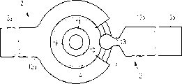
在图1a和1b中所示的芯片引线架2包括一个分成两个电连接部分12a,b的支承部分以及一个热连接部分4。两个电连接部分12a,b分别结束在一个焊接连接条3a,b中。The
一个电连接部分12a具有一个夹环形式的孔,热连接部分4嵌入该孔中。为此,热连接部分4例如可精配合嵌入电连接部分12a中,然后按铆接方式与电连接部分12a挤紧。热连接部分4和电连接部分12a之间的另一类周边连接例如也可通过铆接,钎焊或熔焊来实现。An
热连接部分4基本上是旋转对称的并具有凸起19,这些凸起可实现芯片引线架2牢固锚定在一个外壳中。此外,在热连接部分4中构成一个反射槽16形式的凹坑,在该凹坑的底面设置一个用来安装一个发射辐的芯片的芯片安装区11,而该凹坑的侧面则起反射面的作用。The
电连接部分12a的夹环具有一个空隙13,第二个电连接线12a的一个舌状的引线连接区10与该空隙重叠。这个引线连接区10与反射槽的辐射侧边缘在高度上错开布置。这样,在安装芯片时就可在芯片和引线连接区10之间进行短的引线连接,而无须在热连接部分中在反射槽的边缘上为此设置一个空隙。The clamping ring of the
图2表示本发明一个外壳的一个实施例的纵剖面透视图。该外壳具有一个用塑料模塑材料制成的基体1,该基体例如可周注塑法或压铸法制成。该模塑材料例如由一种以环氧树脂或丙烯酸树脂为基础的塑料材料组成,但了民可由适合于这个目的的别的任何一种材料组成。Figure 2 shows a perspective view in longitudinal section of one embodiment of a housing of the present invention. The housing has a
在基体1中,埋入了一个基本上相当于图1的芯片引线架2,该芯片引线架包括两个电连接部分12a,b和一个嵌入其中的热连接部分4以及焊接连接条,后者从该外壳基体中伸出。热连接部分4在芯片连接区11上构成基本上平面的没有反射槽的结构。In the
热连接部分4是这样布置在外壳基体1内的,使热连接部分4的底面6构成基体支承面7的一部分。该热连接部分在其周边设置有凸起19,以便机械牢固锚定在该外壳基体中。The
在支承面7的对面,在外壳基体中构成一个孔口8作为辐射出射窗口,该孔口通到热连接部分4,这样,一个要固定在其上的发出辐射的芯片便可位于辐射出射窗口8内。辐射发射窗口8的侧面9是倾斜的并作为由这个芯片运行时产生的辐射的反射器用。Opposite the
图3表示本发明一个外壳的另一实施例的支承面的透视图。象前述实施例那样,热连接部分4的底面6从外壳基体1伸出。其中热连接部分4的底面6从基体1稍微凸起,这样,在装配好的状态下,就可保证在热连接部分4和一个相应的支撑体例如一块印制电路板或一个冷却体之间的牢固支承和良好的导热。Figure 3 shows a perspective view of the bearing surface of another embodiment of a housing of the present invention. As in the preceding embodiments, the
与前述实施例不同的是,这个外壳基体1具有一个侧向的、从热连接部分4延伸到外壳基体1的侧面的槽20。当外壳安装到一个支撑体上时。在装配好的状态下,这个槽20也可用来检查该外壳和支撑体之间的连接。这样,就可特别是检查支撑体和热连接部分之间的焊接。In contrast to the preceding exemplary embodiments, this
图4表示本发明一个辐射元件的一个实施例的示意透视图。Figure 4 shows a schematic perspective view of an embodiment of a radiating element of the present invention.
象前述实施例那样,一个芯片引线架2用一个嵌入的热连接部分4几乎埋入外壳基体1中,所以只有焊接连接条3a,b从外壳基体1侧向伸出,热连接部分4以未示出的方式构成外壳基体的支承面7的一部分并由此可从外部进行热连接。Like the previous embodiment, a
在热连接部分4的芯片安装区11上,固定了一个发出辐射的芯片5例如一个发光二极管。最好这是一个半导体芯片,例如一个发光二极管芯片或激光器芯片,该芯片用一种硬焊料焊接到热连接部分4上。另一种方法是,该芯片可用一种粘接剂粘接到芯片安装区11上,该粘接剂应具有足够的导热性,而且最好也是导电的。On the
GaAs、GaP和GaN基的半导体材料例如GaAlAs、InGaAs、InGaAlAs、InGaAlP、GaN、GaAlN、InGaN和InGaAlN特别适合作有效的辐射源。GaAs, GaP and GaN based semiconductor materials such as GaAlAs, InGaAs, InGaAlAs, InGaAlP, GaN, GaAlN, InGaN and InGaAlN are particularly suitable as effective radiation sources.
元件的外壳基本上相当于图2和图3所示的外壳。唯一的区别是,热连接部分4具有一个包围芯片5的反射槽16,它的反射面基本上无缝过渡到辐射出射窗口8的侧面9,所以形成了一个分别由热连接部分4和由辐射出射窗口8构成的区段组成的整个反射器。The housing of the component basically corresponds to the housing shown in FIGS. 2 and 3 . The only difference is that the
此外,辐射出射窗口8在元件的纵向内进行了少许的扩展并包括一个引线连接区10,该连接区位于没有与热连接部分连接的芯片引线架2的电连接部分12b上。一根引线17从这个引线连接区10引到一个设置在芯片5上的接触面。Furthermore, the
引线连接区10与热连接部分的反射槽16的辐射侧的边缘在高度上是错开布置的。这样,在芯片5和引线连接区10之间就可建立短的,因而机械牢固的引线连接,因为后者可靠近芯片5延伸。此外,由此使所产生的引线拱起的高度保持很小,因而减少了短路的危险,这种短路例如在芯片用浇注材料包封时由于引线侧向重叠到热连接部分上而可产生。The lead
图5表示本发明一个元件的另一个实施例的横截面,该横截面相当于沿图4剖面线A-A剖开的轮廓。FIG. 5 shows a cross-section of another embodiment of an element of the invention corresponding to the profile taken along the section line A-A of FIG. 4 .
象图3所示的实施例那样,这里的芯片5的安装侧上的热连接部分也是中心凹入的,所以为芯片5产生的辐射形成了一个反射槽16,辐射出射窗口8的反射侧壁9与该反射槽连接。Like the embodiment shown in Figure 3, the thermal connection part on the mounting side of the
与上述实施例的区别在于,这样构成的整个反射器15在部分反射器9、16之间的过渡部分具有一个折点。通过这种造型使整个反射器15很接近于一个旋转抛物面,并由此达到了有利的辐射特性。与该反射槽的底面以一个较陡的角度从芯片辐射的光线较强地朝元件的主辐射方向偏转。The difference from the above-described exemplary embodiment is that the
为了保护芯片,辐射出射窗口8用一种浇注材料14例如环氧树脂或丙烯酸树脂之类的反应树脂填充。为了产生的辐射的聚束,浇注材料14可象透镜那样构成一个轻微拱起的表面18。To protect the chip, the
为了浇注材料14、外壳基体1和芯片引线架2达到牢固的机械连接,热连接部分的反射槽16的高度A最好选用小于芯片5的两倍高度H。由热连接部分4和外壳基体1构成的整个反射器15的高度B应小于芯片5的4倍高度H。最后,辐射出射窗口8最好这样造型,使浇注的体积V满足上述关系:In order to achieve a firm mechanical connection between the potting
V≤q·HV≤q·H
式中q约为7毫米2。由于满足了这个关系,便有利于增加机械稳定性并由此提高元件的容许负荷和寿命。为此,把热连接部分4用凸起19锚定在外壳基体1中同样有助于这个目的。In the formula, q is about 7 mm 2 . Since this relationship is satisfied, it is advantageous to increase the mechanical stability and thus the permissible load and life of the component. For this purpose, the anchoring of the
为了制作这种元件,首先要为芯片引线架2制备一个支承部分,该支承部分例如用一种支承带冲压而成并带有一个孔。然后将热连接部分4嵌入该支承部分的这个孔中并与该支承部分挤紧。In order to produce such a component, first a carrier part is prepared for the
在下一个步骤中,在热连接部分4上安装例如焊接或粘接发出辐射的芯片5。为了构成外壳基体1,由该支承部分和热连接部分4构成的芯片引线架2与预安装的芯片5用一种模塑材料进行包封,其中,芯片5周围的区域以及引线连接区10留有空隙。这种包封例如可用注塑法或压铸法来实现。最后,将一根引线17从引线连接区10引到芯片5的一个接触面。In a next step, a radiation-emitting
另一种办法是,在该支承部分和热连接部分4连接后,首先用上述模塑材料包封所构成的芯片引线架2,然后将芯片5固定最好粘接并键合到芯片连接区11上。Another way is, after the support part and the
当然,本发明结合实施例进行的说明并不表示本发明局限于这些实施例。本发明的芯片引线架和外壳在很大程度上可用于要求有效散热的其他元件,或作为芯片也可用其他的半导体。Of course, the description of the present invention in conjunction with the embodiments does not mean that the present invention is limited to these embodiments. The chip lead frame and housing of the present invention can be used to a large extent in other components requiring effective heat dissipation, or other semiconductors can also be used as chips.
上述方法包括制备一个芯片引线架的步骤和该芯片最好通过焊接固定是在芯片引线架用一种模塑材料包封之前进行的,其中芯片的周围留有空隙,也可应用到其他外壳结构型式上而不用热连接部分,这本身就已经是一种发明。The method described above includes the steps of preparing a chip lead frame and fixing the chip preferably by soldering before the chip lead frame is encapsulated with a molding material, wherein the chip is surrounded by voids, and can also be applied to other housing structures It is already an invention in itself to eliminate the need for thermal connection parts.
这种方法的诸多优点特别在于,芯片的固定可达到最佳化而几乎与模塑材料的性能无关。焊接过程例如可在一个扩展的温度区进行,而且焊料可用熔点最好超过260℃的例如硬焊料,这种焊料可在芯片和芯片引线架之间建立热阻很小的连接。这样,也就减少了在一个相应元件分离到一块印制电路板上时芯片可能松脱的危险。The advantages of this method are in particular that the fixation of the chips can be optimized almost independently of the properties of the molding material. The soldering process can be carried out, for example, in an extended temperature range, and the solder can preferably have a melting point above 260° C., such as hard solder, which can establish a connection with low thermal resistance between the chip and the chip lead frame. In this way, the risk that the chip may come loose when a corresponding component is separated onto a printed circuit board is reduced.
Claims (38)
Applications Claiming Priority (2)
| Application Number | Priority Date | Filing Date | Title |
|---|---|---|---|
| DE10117889A DE10117889A1 (en) | 2001-04-10 | 2001-04-10 | Leadframe used for a light emitting diode component comprises a chip assembly region, a wire connecting region, external electrical connecting strips, and a support part coupled with a thermal connecting part |
| DE10117889.1 | 2001-04-10 |
Related Child Applications (1)
| Application Number | Title | Priority Date | Filing Date |
|---|---|---|---|
| CN200710185051.6A Division CN100539225C (en) | 2001-04-10 | 2002-04-09 | Housing of radiating element, radiating element and manufacturing method thereof |
Publications (2)
| Publication Number | Publication Date |
|---|---|
| CN1602555A true CN1602555A (en) | 2005-03-30 |
| CN100359702C CN100359702C (en) | 2008-01-02 |
Family
ID=7681095
Family Applications (2)
| Application Number | Title | Priority Date | Filing Date |
|---|---|---|---|
| CNB028116631A Expired - Lifetime CN100359702C (en) | 2001-04-10 | 2002-04-09 | Chip lead frame of radiation element, radiation element and manufacturing method thereof |
| CN200710185051.6A Expired - Lifetime CN100539225C (en) | 2001-04-10 | 2002-04-09 | Housing of radiating element, radiating element and manufacturing method thereof |
Family Applications After (1)
| Application Number | Title | Priority Date | Filing Date |
|---|---|---|---|
| CN200710185051.6A Expired - Lifetime CN100539225C (en) | 2001-04-10 | 2002-04-09 | Housing of radiating element, radiating element and manufacturing method thereof |
Country Status (7)
| Country | Link |
|---|---|
| US (1) | US8097937B2 (en) |
| EP (1) | EP1378013B1 (en) |
| JP (2) | JP2004521506A (en) |
| CN (2) | CN100359702C (en) |
| DE (1) | DE10117889A1 (en) |
| TW (1) | TW550775B (en) |
| WO (1) | WO2002084749A2 (en) |
Cited By (7)
| Publication number | Priority date | Publication date | Assignee | Title |
|---|---|---|---|---|
| US8070316B2 (en) | 2005-12-22 | 2011-12-06 | Panasonic Electric Works Co., Ltd. | Lighting apparatus with LEDs |
| CN101300688B (en) * | 2005-08-30 | 2012-04-04 | 奥斯兰姆奥普托半导体有限责任公司 | Surface-mountable optoelectronic device and method of manufacturing the same |
| CN102714267A (en) * | 2009-11-19 | 2012-10-03 | 住友化学株式会社 | Package for semiconductor, and heat dissipating lead frame |
| CN102918669A (en) * | 2010-05-27 | 2013-02-06 | 欧司朗光电半导体有限公司 | Optoelectronic component and method for producing an optoelectronic component and a compound structure |
| CN103700635A (en) * | 2013-12-25 | 2014-04-02 | 北京必创科技有限公司 | Chip packaging structure with cavity and packaging method thereof |
| US10096756B2 (en) | 2005-11-25 | 2018-10-09 | Samsung Electronics Co., Ltd. | Side view light emitting diode package |
| TWI659510B (en) * | 2016-10-14 | 2019-05-11 | Omron Corporation | Electronic device and manufacturing method thereof |
Families Citing this family (163)
| Publication number | Priority date | Publication date | Assignee | Title |
|---|---|---|---|---|
| DE10131698A1 (en) * | 2001-06-29 | 2003-01-30 | Osram Opto Semiconductors Gmbh | Surface-mountable radiation-emitting component and method for its production |
| DE10243247A1 (en) * | 2002-09-17 | 2004-04-01 | Osram Opto Semiconductors Gmbh | Leadframe-based component housing, leadframe tape, surface-mountable electronic component and method of manufacture |
| US7692206B2 (en) * | 2002-12-06 | 2010-04-06 | Cree, Inc. | Composite leadframe LED package and method of making the same |
| EP1597764A1 (en) * | 2003-02-28 | 2005-11-23 | Osram Opto Semiconductors GmbH | Optoelectronic component comprising a housing body which is metallised in a structured manner, method for producing one such component, and method for the structured metallisation of a body containing plastic |
| FR2853200B1 (en) * | 2003-03-27 | 2005-10-07 | Valeo Vision | METHOD FOR FIXING A POWER LIGHT EMITTING DIODE ON A RADIATOR, AND A SIGNALING DEVICE COMPRISING SUCH A DIODE |
| USD509195S1 (en) * | 2003-04-08 | 2005-09-06 | Harvatek Corporation | Light emitting diode package |
| JP4599857B2 (en) * | 2003-04-24 | 2010-12-15 | 日亜化学工業株式会社 | Semiconductor device and manufacturing method thereof |
| JP4600404B2 (en) * | 2003-04-24 | 2010-12-15 | 日亜化学工業株式会社 | Semiconductor device and manufacturing method thereof |
| DE10323857A1 (en) | 2003-05-26 | 2005-01-27 | Osram Opto Semiconductors Gmbh | Housing for a laser diode device, laser diode device and method of manufacturing a laser diode device |
| JP4966656B2 (en) | 2003-05-28 | 2012-07-04 | ソウル半導体株式会社 | Light emitting diode package with multiple heat sinks |
| JP4645071B2 (en) | 2003-06-20 | 2011-03-09 | 日亜化学工業株式会社 | Package molded body and semiconductor device using the same |
| DE102004034166B4 (en) | 2003-07-17 | 2015-08-20 | Toyoda Gosei Co., Ltd. | Light-emitting device |
| DE10347737A1 (en) * | 2003-09-30 | 2005-05-04 | Osram Opto Semiconductors Gmbh | Optoelectronic structural element with a semiconductor body, including a substrate, a layer system deposited on the substrate and a metallized carrier useful in thin film, Flip-Chip and semiconductor technology |
| EP1521312A3 (en) * | 2003-09-30 | 2008-01-16 | Osram Opto Semiconductors GmbH | Optoelectronic device having a metallised carrier |
| EP1544923A3 (en) * | 2003-12-19 | 2007-03-14 | Osram Opto Semiconductors GmbH | Radiation emitting semiconductor device and method of mounting a semiconductor chip on a leadframe |
| US7321161B2 (en) * | 2003-12-19 | 2008-01-22 | Philips Lumileds Lighting Company, Llc | LED package assembly with datum reference feature |
| JP4274935B2 (en) * | 2003-12-26 | 2009-06-10 | トキコーポレーション株式会社 | Case for light emitting unit and method for manufacturing light emitting unit |
| DE102004003928B4 (en) * | 2004-01-26 | 2012-02-23 | Tay Kheng Chiong | A miniaturized SM-technology optoelectronic device and method of making this device |
| DE102004003929B8 (en) * | 2004-01-26 | 2016-03-10 | Dominant Opto Technologies Sdn Bhd | SM-technology optoelectronic component |
| DE102004009284A1 (en) | 2004-02-26 | 2005-09-15 | Osram Opto Semiconductors Gmbh | Light-emitting diode arrangement for a high-performance light-emitting diode and method for producing a light-emitting diode arrangement |
| JP4525193B2 (en) * | 2004-06-15 | 2010-08-18 | パナソニック株式会社 | Package for optical semiconductor element and light emitting device using the same |
| DE102004031685A1 (en) * | 2004-06-30 | 2006-01-19 | Osram Opto Semiconductors Gmbh | Housing for an optoelectronic component has central heat dissipating element with central thermal contact region surrounded by ring of chip mounting surfaces |
| KR100707958B1 (en) * | 2004-07-20 | 2007-04-18 | 두림시스템 주식회사 | Surface Mount Light Emitting Device, Package Structure and Manufacturing Method Thereof |
| DE102004051379A1 (en) * | 2004-08-23 | 2006-03-23 | Osram Opto Semiconductors Gmbh | Device for an optoelectronic component and component with an optoelectronic component and a device |
| DE102004042186B4 (en) * | 2004-08-31 | 2010-07-01 | Osram Opto Semiconductors Gmbh | Optoelectronic component |
| KR100587020B1 (en) | 2004-09-01 | 2006-06-08 | 삼성전기주식회사 | High power light emitting diode package |
| DE102004043516A1 (en) | 2004-09-08 | 2006-03-23 | Osram Opto Semiconductors Gmbh | Laterally emitting, radiation generating component with radiation source, whose optical axis extends orthogonally to assembly surface of component |
| WO2006059828A1 (en) * | 2004-09-10 | 2006-06-08 | Seoul Semiconductor Co., Ltd. | Light emitting diode package having multiple molding resins |
| TWI257992B (en) * | 2004-09-13 | 2006-07-11 | Neobulb Technologies Inc | Lighting device with highly efficient heat dissipation structure |
| DE102004045950A1 (en) | 2004-09-22 | 2006-03-30 | Osram Opto Semiconductors Gmbh | Housing for an optoelectronic component, optoelectronic component and method for producing an optoelectronic component |
| JP2006108333A (en) * | 2004-10-04 | 2006-04-20 | Toyoda Gosei Co Ltd | lamp |
| JP5060707B2 (en) * | 2004-11-10 | 2012-10-31 | 日立化成工業株式会社 | Thermosetting resin composition for light reflection |
| GB2420221B (en) * | 2004-11-12 | 2009-09-09 | Unity Opto Technology Co Ltd | Solid-state semiconductor light emitting device |
| WO2006098545A2 (en) * | 2004-12-14 | 2006-09-21 | Seoul Opto Device Co., Ltd. | Light emitting device having a plurality of light emitting cells and package mounting the same |
| WO2006065007A1 (en) * | 2004-12-16 | 2006-06-22 | Seoul Semiconductor Co., Ltd. | Leadframe having a heat sink supporting ring, fabricating method of a light emitting diodepackage using the same and light emitting diodepackage fabbricated by the method |
| US7777247B2 (en) * | 2005-01-14 | 2010-08-17 | Cree, Inc. | Semiconductor light emitting device mounting substrates including a conductive lead extending therein |
| JP4698234B2 (en) * | 2005-01-21 | 2011-06-08 | スタンレー電気株式会社 | Surface mount semiconductor device |
| DE102005019115B4 (en) * | 2005-01-24 | 2010-04-08 | Osram Opto Semiconductors Gmbh | Semiconductor laser device |
| KR100631901B1 (en) * | 2005-01-31 | 2006-10-11 | 삼성전기주식회사 | LED package frame and LED package employing the same |
| DE102005041065A1 (en) | 2005-02-16 | 2006-08-24 | Patent-Treuhand-Gesellschaft für elektrische Glühlampen mbH | lighting device |
| KR100631903B1 (en) * | 2005-02-17 | 2006-10-11 | 삼성전기주식회사 | High power LED housing and its manufacturing method |
| KR100665117B1 (en) | 2005-02-17 | 2007-01-09 | 삼성전기주식회사 | LED housing and manufacturing method thereof |
| DE102005020908A1 (en) | 2005-02-28 | 2006-08-31 | Osram Opto Semiconductors Gmbh | Lighting device for back lighting of liquid crystal display, has optical unit with radiation emission surface which has convex curved partial region that partially surrounds concave curved partial region in distance to optical axis |
| KR101161384B1 (en) * | 2005-03-29 | 2012-07-02 | 서울반도체 주식회사 | Led package mounting a led having an array of light emitting cells coupled in series |
| EP2280430B1 (en) | 2005-03-11 | 2020-01-01 | Seoul Semiconductor Co., Ltd. | LED package having an array of light emitting cells coupled in series |
| US7977698B2 (en) * | 2005-03-18 | 2011-07-12 | Avago Technologies Ecbu Ip (Singapore) Pte. Ltd. | System and method for surface mountable display |
| ATE410483T1 (en) * | 2005-05-26 | 2008-10-15 | Dow Corning | METHOD AND SILICONE ENCAPSULATING COMPOSITION FOR FORMING SMALL SHAPES |
| KR100593945B1 (en) * | 2005-05-30 | 2006-06-30 | 삼성전기주식회사 | High output LED package and manufacturing method |
| KR100616684B1 (en) * | 2005-06-03 | 2006-08-28 | 삼성전기주식회사 | High output LED package and manufacturing method |
| US20060289887A1 (en) * | 2005-06-24 | 2006-12-28 | Jabil Circuit, Inc. | Surface mount light emitting diode (LED) assembly with improved power dissipation |
| TWI287300B (en) * | 2005-06-30 | 2007-09-21 | Lite On Technology Corp | Semiconductor package structure |
| KR100631992B1 (en) * | 2005-07-19 | 2006-10-09 | 삼성전기주식회사 | Side-emitting dual lens structure LED package |
| DE102005034166A1 (en) * | 2005-07-21 | 2007-02-01 | Osram Opto Semiconductors Gmbh | Housing for an electromagnetic radiation-emitting optoelectronic component, electromagnetic radiation-emitting component and method for producing a housing or a component |
| DE102005036077A1 (en) * | 2005-08-01 | 2007-04-26 | Epcos Ag | Tranformator arrangement with a piezotransformer |
| KR100632003B1 (en) | 2005-08-08 | 2006-10-09 | 삼성전기주식회사 | LED package with recessed part in heat transfer part |
| KR100629496B1 (en) * | 2005-08-08 | 2006-09-28 | 삼성전자주식회사 | LED package and manufacturing method thereof |
| DE102006020529A1 (en) * | 2005-08-30 | 2007-03-01 | Osram Opto Semiconductors Gmbh | Optoelectronic component has semiconductor body emitting electromagnetic radiation that passes through an optical element comprising wavelength conversion material |
| DE102005046450A1 (en) | 2005-09-28 | 2007-04-05 | Osram Opto Semiconductors Gmbh | Optoelectronic semiconductor chip, method for its production and optoelectronic component |
| DE102005061208A1 (en) | 2005-09-30 | 2007-04-12 | Osram Opto Semiconductors Gmbh | lighting device |
| JP5303097B2 (en) * | 2005-10-07 | 2013-10-02 | 日立化成株式会社 | Thermosetting light reflecting resin composition, optical semiconductor mounting substrate using the same, manufacturing method thereof, and optical semiconductor device. |
| US8100567B2 (en) * | 2005-10-19 | 2012-01-24 | Rambus International Ltd. | Light-emitting devices and related systems |
| TW200729437A (en) | 2005-10-20 | 2007-08-01 | Creative Led Gmbh | Package casing for semiconductor chip and heat dissipation structure thereof |
| JP2007157940A (en) * | 2005-12-02 | 2007-06-21 | Nichia Chem Ind Ltd | Light emitting device and method for manufacturing light emitting device |
| DE102006010729A1 (en) | 2005-12-09 | 2007-06-14 | Osram Opto Semiconductors Gmbh | Optical component, e.g. for miniature opto-electronic semi-conductor chips, comprises a composite unit of lens and mounting part in different materials |
| WO2007069399A1 (en) | 2005-12-12 | 2007-06-21 | Nichia Corporation | Light emitting device, semiconductor device, and its manufacturing method |
| WO2007086987A1 (en) * | 2006-01-17 | 2007-08-02 | Dow Corning Corporation | Thermally stable transparent silicone resin compositions and methods for their preparation and use |
| CN101336383B (en) * | 2006-02-01 | 2012-05-09 | 陶氏康宁公司 | Impact resistant optical waveguide and method of making same |
| DE102006004581A1 (en) * | 2006-02-01 | 2007-08-09 | Patent-Treuhand-Gesellschaft für elektrische Glühlampen mbH | Light module, multiple light module and use of a light module or multiple light module for illumination or backlighting |
| US8258502B2 (en) * | 2006-02-24 | 2012-09-04 | Dow Corning Corporation | Light emitting device encapsulated with silicones and curable silicone compositions for preparing the silicones |
| US20070211182A1 (en) * | 2006-03-10 | 2007-09-13 | Luminus Devices, Inc. | Optical system thermal management methods and systems |
| WO2007106327A2 (en) * | 2006-03-10 | 2007-09-20 | Luminus Devices, Inc. | Lcd thermal management methods and systems |
| US20070211183A1 (en) * | 2006-03-10 | 2007-09-13 | Luminus Devices, Inc. | LCD thermal management methods and systems |
| US20070211184A1 (en) * | 2006-03-10 | 2007-09-13 | Luminus Devices, Inc. | Liquid crystal display systems including LEDs |
| WO2007135707A1 (en) | 2006-05-18 | 2007-11-29 | Nichia Corporation | Resin molded body and surface-mounted light emitting device, and manufacturing method thereof |
| DE602006010826D1 (en) | 2006-05-19 | 2010-01-14 | Osram Gmbh | Optoelectronic module and lighting device with such a module |
| KR100904152B1 (en) | 2006-06-30 | 2009-06-25 | 서울반도체 주식회사 | Leadframe having a heat sink supporting part, fabricating method of the light emitting diode package using the same and light emitting diode package fabricated by the method |
| DE102006035635A1 (en) | 2006-07-31 | 2008-02-07 | Osram Opto Semiconductors Gmbh | lighting arrangement |
| TWI418054B (en) * | 2006-08-08 | 2013-12-01 | Lg電子股份有限公司 | Light emitting device package and method of manufacturing the same |
| KR101163492B1 (en) | 2006-08-08 | 2012-07-18 | 엘지이노텍 주식회사 | LED package |
| DE102006046678A1 (en) * | 2006-09-29 | 2008-04-03 | Osram Opto Semiconductors Gmbh | Housing for use with semiconductor body of e.g. LED unit, has plastic-base body with plastic components, where one plastic component is made of material differing from that of other component in optical characteristic |
| KR101248514B1 (en) * | 2006-09-29 | 2013-04-04 | 서울반도체 주식회사 | Led package and its fabricating method, and dish reflector used for the same |
| US8497560B2 (en) * | 2006-10-06 | 2013-07-30 | Industrial Technology Research Institute | LED package and method of assembling the same |
| DE102006048230B4 (en) | 2006-10-11 | 2012-11-08 | Osram Ag | Light-emitting diode system, method for producing such and backlighting device |
| TW200820455A (en) * | 2006-10-18 | 2008-05-01 | Young Lighting Technology Corp | LED package and manufacture method thereof |
| JP4961978B2 (en) * | 2006-11-30 | 2012-06-27 | 日亜化学工業株式会社 | Light emitting device and manufacturing method thereof |
| DE102007001706A1 (en) | 2007-01-11 | 2008-07-17 | Osram Opto Semiconductors Gmbh | Housing for optoelectronic component and arrangement of an optoelectronic component in a housing |
| DE102007017113A1 (en) | 2007-01-31 | 2008-08-07 | Osram Opto Semiconductors Gmbh | Semiconductor device with an optically active layer, arrangement with a plurality of optically active layers and method for producing a semiconductor device |
| EP1953837A3 (en) | 2007-01-31 | 2014-01-15 | OSRAM Opto Semiconductors GmbH | Semiconductor component with an optically active layer, assembly with a number of optically active layers and method for producing a semiconductor component |
| US8604506B2 (en) * | 2007-02-22 | 2013-12-10 | Sharp Kabushiki Kaisha | Surface mounting type light emitting diode and method for manufacturing the same |
| US8092064B2 (en) * | 2007-02-23 | 2012-01-10 | Rambus International Ltd. | Tiled illumination assembly and related methods |
| DE102007021904A1 (en) * | 2007-02-28 | 2008-09-04 | Osram Opto Semiconductors Gmbh | Housing body for opto-electronic component, has main surface with surface area and another surface area, and both surface areas are adjoined together by outer edge |
| TW200843130A (en) * | 2007-04-17 | 2008-11-01 | Wen Lin | Package structure of a surface-mount high-power light emitting diode chip and method of making the same |
| DE102007023918A1 (en) | 2007-05-23 | 2008-11-27 | Siemens Ag Österreich | lighting unit |
| DE102007043904A1 (en) | 2007-09-14 | 2009-03-19 | Osram Gesellschaft mit beschränkter Haftung | Luminous device |
| DE102007043903A1 (en) | 2007-09-14 | 2009-03-26 | Osram Gesellschaft mit beschränkter Haftung | Luminous device |
| TWI352439B (en) * | 2007-09-21 | 2011-11-11 | Lite On Technology Corp | Light emitting diode packaging device, heat-dissip |
| DE102008021618A1 (en) * | 2007-11-28 | 2009-06-04 | Osram Opto Semiconductors Gmbh | Chip arrangement, connection arrangement, LED and method for producing a chip arrangement |
| US20090218588A1 (en) * | 2007-12-06 | 2009-09-03 | Paul Panaccione | Chip-scale packaged light-emitting devices |
| DE102008003971A1 (en) * | 2008-01-11 | 2009-07-16 | Ledon Lighting Jennersdorf Gmbh | Light-emitting diode arrangement with protective frame |
| JPWO2009090988A1 (en) * | 2008-01-16 | 2011-05-26 | 古河電気工業株式会社 | Optical module |
| DE102008029191A1 (en) | 2008-01-31 | 2009-08-06 | Osram Opto Semiconductors Gmbh | Illumination device for backlighting a display and a display with such a lighting device |
| TWI351777B (en) * | 2008-04-22 | 2011-11-01 | Silicon Base Dev Inc | Bade for light diode and its manufacturing method |
| JP5217800B2 (en) | 2008-09-03 | 2013-06-19 | 日亜化学工業株式会社 | Light emitting device, resin package, resin molded body, and manufacturing method thereof |
| DE102008045925A1 (en) * | 2008-09-04 | 2010-03-11 | Osram Opto Semiconductors Gmbh | Optoelectronic component and method for producing an optoelectronic component |
| KR100982994B1 (en) * | 2008-10-15 | 2010-09-17 | 삼성엘이디 주식회사 | LED Package Module |
| CN102077371B (en) | 2008-11-07 | 2012-10-31 | 凸版印刷株式会社 | Lead frame, manufacturing method thereof, and semiconductor light emitting device using lead frame |
| DE102008059552A1 (en) | 2008-11-28 | 2010-06-02 | Osram Opto Semiconductors Gmbh | Light-emitting diode module and light-emitting diode component |
| US8598602B2 (en) * | 2009-01-12 | 2013-12-03 | Cree, Inc. | Light emitting device packages with improved heat transfer |
| US7923739B2 (en) | 2009-06-05 | 2011-04-12 | Cree, Inc. | Solid state lighting device |
| US8860043B2 (en) | 2009-06-05 | 2014-10-14 | Cree, Inc. | Light emitting device packages, systems and methods |
| US8686445B1 (en) | 2009-06-05 | 2014-04-01 | Cree, Inc. | Solid state lighting devices and methods |
| US9111778B2 (en) | 2009-06-05 | 2015-08-18 | Cree, Inc. | Light emitting diode (LED) devices, systems, and methods |
| DE102009036621B4 (en) | 2009-08-07 | 2023-12-21 | OSRAM Opto Semiconductors Gesellschaft mit beschränkter Haftung | Optoelectronic semiconductor component |
| KR101014063B1 (en) | 2009-08-26 | 2011-02-10 | 엘지이노텍 주식회사 | Light emitting element and light unit using same |
| JP5936810B2 (en) | 2009-09-11 | 2016-06-22 | ローム株式会社 | Light emitting device |
| CN102034782A (en) * | 2009-09-30 | 2011-04-27 | 万国半导体有限公司 | Mixed alloy lead frame used for power semiconductors |
| DE102009047882A1 (en) | 2009-09-30 | 2011-03-31 | Osram Opto Semiconductors Gmbh | LED traffic signal |
| US8120056B2 (en) * | 2009-10-19 | 2012-02-21 | Avago Technologies Ecbu Ip (Singapore) Pte. Ltd. | Light emitting diode assembly |
| DE102009054474A1 (en) * | 2009-12-10 | 2011-06-16 | Osram Gesellschaft mit beschränkter Haftung | Light module and light chain |
| JP5010716B2 (en) | 2010-01-29 | 2012-08-29 | 株式会社東芝 | LED package |
| JP5010693B2 (en) | 2010-01-29 | 2012-08-29 | 株式会社東芝 | LED package |
| US8525213B2 (en) * | 2010-03-30 | 2013-09-03 | Lg Innotek Co., Ltd. | Light emitting device having multiple cavities and light unit having the same |
| KR101161399B1 (en) * | 2010-04-27 | 2012-07-02 | 서울반도체 주식회사 | Led package mounting a led chip |
| JP2010212717A (en) * | 2010-04-30 | 2010-09-24 | Hitachi Chem Co Ltd | Substrate for mounting optical semiconductor using light-reflecting thermosetting resin composition, method for manufacturing the same, and optical semiconductor device |
| US8269244B2 (en) | 2010-06-28 | 2012-09-18 | Cree, Inc. | LED package with efficient, isolated thermal path |
| US8648359B2 (en) | 2010-06-28 | 2014-02-11 | Cree, Inc. | Light emitting devices and methods |
| USD643819S1 (en) | 2010-07-16 | 2011-08-23 | Cree, Inc. | Package for light emitting diode (LED) lighting |
| CN102339941A (en) * | 2010-07-28 | 2012-02-01 | 展晶科技(深圳)有限公司 | Light emitting diode packaging structure and light emitting diode module |
| US8860209B1 (en) | 2010-08-16 | 2014-10-14 | NuLEDs, Inc. | LED luminaire having front and rear convective heat sinks |
| US8585248B1 (en) | 2010-08-16 | 2013-11-19 | NuLEDs, Inc. | LED luminaire having heat sinking panels |
| US8079139B1 (en) * | 2010-08-27 | 2011-12-20 | I-Chiun Precision Industry Co., Ltd. | Method for producing electro-thermal separation type light emitting diode support structure |
| KR101677105B1 (en) * | 2010-08-30 | 2016-11-17 | 삼성디스플레이 주식회사 | Electronic component and manufacturing method for the same |
| US9070851B2 (en) | 2010-09-24 | 2015-06-30 | Seoul Semiconductor Co., Ltd. | Wafer-level light emitting diode package and method of fabricating the same |
| TW201220555A (en) * | 2010-11-02 | 2012-05-16 | Hon Hai Prec Ind Co Ltd | Light emitting diode lead frame |
| JP2014038876A (en) * | 2010-12-15 | 2014-02-27 | Panasonic Corp | Semiconductor light-emitting device |
| US11101408B2 (en) | 2011-02-07 | 2021-08-24 | Creeled, Inc. | Components and methods for light emitting diode (LED) lighting |
| US8610140B2 (en) | 2010-12-15 | 2013-12-17 | Cree, Inc. | Light emitting diode (LED) packages, systems, devices and related methods |
| USD679842S1 (en) | 2011-01-03 | 2013-04-09 | Cree, Inc. | High brightness LED package |
| JP5714916B2 (en) * | 2011-01-12 | 2015-05-07 | ルネサスエレクトロニクス株式会社 | Semiconductor device and manufacturing method thereof |
| TW201251140A (en) | 2011-01-31 | 2012-12-16 | Cree Inc | High brightness light emitting diode (LED) packages, systems and methods with improved resin filling and high adhesion |
| DE102011013277A1 (en) * | 2011-03-07 | 2012-09-13 | Schott Ag | Housing for high-performance light-emitting diodes - "2-layer system" |
| KR101852388B1 (en) | 2011-04-28 | 2018-04-26 | 엘지이노텍 주식회사 | Light emitting device package |
| US20160277017A1 (en) * | 2011-09-13 | 2016-09-22 | Fsp Technology Inc. | Snubber circuit |
| KR101374899B1 (en) * | 2012-01-13 | 2014-03-17 | 서울반도체 주식회사 | Light emitting diode |
| JP5376014B2 (en) * | 2012-07-03 | 2013-12-25 | 日立化成株式会社 | A thermosetting resin composition for light reflection, an optical semiconductor mounting substrate using the same, a manufacturing method thereof, and an optical semiconductor device. |
| JP2013012763A (en) * | 2012-08-24 | 2013-01-17 | Hitachi Chem Co Ltd | Thermosetting resin composition for light reflection, optical semiconductor mounting substrate manufactured using the same, method for manufacturing the substrate, and optical semiconductor device |
| KR102029802B1 (en) * | 2013-01-14 | 2019-10-08 | 엘지이노텍 주식회사 | Light emitting device and light apparatus having thereof |
| CN104937326B (en) * | 2013-01-25 | 2018-10-26 | 亮锐控股有限公司 | Light fixture and method for manufacturing light fixture |
| US20140208689A1 (en) | 2013-01-25 | 2014-07-31 | Renee Joyal | Hypodermic syringe assist apparatus and method |
| KR102222580B1 (en) | 2014-07-30 | 2021-03-05 | 삼성전자주식회사 | Light emitting device package and display device including the same |
| JP6557968B2 (en) * | 2014-12-25 | 2019-08-14 | 日亜化学工業株式会社 | Package, light emitting device and manufacturing method thereof |
| CN105575921A (en) * | 2016-02-29 | 2016-05-11 | 卓广实业(上海)有限公司 | IC component for vertical heat conduction package structure |
| CN205944139U (en) | 2016-03-30 | 2017-02-08 | 首尔伟傲世有限公司 | Ultraviolet ray light -emitting diode spare and contain this emitting diode module |
| USD803795S1 (en) * | 2016-08-09 | 2017-11-28 | Rsm Electron Power, Inc. | Surface mount device |
| USD803796S1 (en) * | 2016-08-09 | 2017-11-28 | Rsm Electron Power, Inc. | Surface mount device |
| USD803798S1 (en) * | 2016-08-09 | 2017-11-28 | Rsm Electron Power, Inc. | Surface mount device |
| USD803797S1 (en) * | 2016-08-09 | 2017-11-28 | Rsm Electron Power, Inc. | Surface mount device |
| TWI713239B (en) * | 2016-12-01 | 2020-12-11 | 晶元光電股份有限公司 | Light-emitting device |
| CN108540086A (en) * | 2018-01-18 | 2018-09-14 | 浙江人和光伏科技有限公司 | A kind of conductive module of solar battery connecting box |
| TWI713237B (en) * | 2018-08-01 | 2020-12-11 | 大陸商光寶光電(常州)有限公司 | Led package structure |
| CN110798961B (en) * | 2018-08-01 | 2022-10-21 | 苏州旭创科技有限公司 | Circuit board and optical module with same |
| JP7337590B2 (en) * | 2019-08-05 | 2023-09-04 | ローム株式会社 | semiconductor light emitting device |
| DE102021108604A1 (en) | 2021-04-07 | 2022-10-13 | OSRAM Opto Semiconductors Gesellschaft mit beschränkter Haftung | DEVICE WITH STRUCTURED LEAD FRAME AND HOUSING BODY AND METHOD OF MAKING THE DEVICE |
Family Cites Families (57)
| Publication number | Priority date | Publication date | Assignee | Title |
|---|---|---|---|---|
| JPS518783B2 (en) * | 1971-11-10 | 1976-03-19 | ||
| US3780357A (en) * | 1973-02-16 | 1973-12-18 | Hewlett Packard Co | Electroluminescent semiconductor display apparatus and method of fabricating the same |
| DE2315709A1 (en) * | 1973-03-29 | 1974-10-10 | Licentia Gmbh | RADIATION-EMISSING SEMI-CONDUCTOR ARRANGEMENT WITH HIGH RADIATION POWER |
| JPS58218153A (en) * | 1982-06-14 | 1983-12-19 | Hitachi Cable Ltd | Lead frame for semiconductor |
| JPS6135576A (en) | 1984-07-27 | 1986-02-20 | Toshiba Corp | Semiconductor light-emitting device |
| JPH0414944Y2 (en) * | 1985-07-19 | 1992-04-03 | ||
| JPH0414945Y2 (en) * | 1985-07-29 | 1992-04-03 | ||
| JPH01129424A (en) | 1987-11-15 | 1989-05-22 | Omron Tateisi Electron Co | Resin sealing of electronic element |
| JPH0256956A (en) | 1988-08-22 | 1990-02-26 | Mitsui Petrochem Ind Ltd | Electronic part, sealing medium for electronic part and sealing method |
| JPH02187058A (en) * | 1989-01-13 | 1990-07-23 | Hitachi Ltd | Semiconductor device package |
| JPH03286588A (en) * | 1990-04-03 | 1991-12-17 | Sumitomo Metal Ind Ltd | Compound semiconductor device |
| DE4017697C2 (en) * | 1990-06-01 | 2003-12-11 | Bosch Gmbh Robert | Electronic component, process for its production and use |
| US5202288A (en) * | 1990-06-01 | 1993-04-13 | Robert Bosch Gmbh | Method of manufacturing an electronic circuit component incorporating a heat sink |
| US5218215A (en) * | 1990-12-19 | 1993-06-08 | Vlsi Technology, Inc. | Semiconductor device package having a thermal dissipation means that allows for lateral movement of the lead frame with respect to the housing without breakage of the thermal dissipation path |
| JPH0517680U (en) * | 1991-08-13 | 1993-03-05 | 日本信号株式会社 | Light emitting diode indicator |
| JP2989703B2 (en) * | 1991-10-08 | 1999-12-13 | シャープ株式会社 | Chip component type light emitting diode |
| US5608267A (en) * | 1992-09-17 | 1997-03-04 | Olin Corporation | Molded plastic semiconductor package including heat spreader |
| JP3227295B2 (en) * | 1993-12-28 | 2001-11-12 | 松下電工株式会社 | Light emitting diode manufacturing method |
| JP3269251B2 (en) * | 1994-03-31 | 2002-03-25 | 株式会社デンソー | Manufacturing method of stacked semiconductor device |
| JPH07283441A (en) | 1994-04-15 | 1995-10-27 | Toshiba Corp | Optical semiconductor device and manufacturing method thereof |
| JPH07307492A (en) | 1994-05-11 | 1995-11-21 | Mitsubishi Cable Ind Ltd | LED assembly module and manufacturing method thereof |
| US5542175A (en) * | 1994-12-20 | 1996-08-06 | International Business Machines Corporation | Method of laminating and circuitizing substrates having openings therein |
| KR100214463B1 (en) * | 1995-12-06 | 1999-08-02 | 구본준 | Lead frame of clip type and method manufacture of the package |
| US5650663A (en) * | 1995-07-03 | 1997-07-22 | Olin Corporation | Electronic package with improved thermal properties |
| DE19536454B4 (en) * | 1995-09-29 | 2006-03-09 | Osram Opto Semiconductors Gmbh | Optoelectronic semiconductor device |
| DE19549818B4 (en) * | 1995-09-29 | 2010-03-18 | Osram Opto Semiconductors Gmbh | Optoelectronic semiconductor device |
| DE19536463C2 (en) * | 1995-09-29 | 2002-02-07 | Infineon Technologies Ag | Method of manufacturing a plurality of laser diode devices |
| DE19545675A1 (en) * | 1995-12-07 | 1997-06-12 | Sel Alcatel Ag | Synchronous digital transmission system |
| JPH09260568A (en) * | 1996-03-27 | 1997-10-03 | Mitsubishi Electric Corp | Semiconductor device and manufacturing method thereof |
| DE19625384A1 (en) * | 1996-06-25 | 1998-01-02 | Siemens Ag | Compound lead frame |
| WO1998020718A1 (en) * | 1996-11-06 | 1998-05-14 | Siliconix Incorporated | Heat sink-lead frame structure |
| JP3856250B2 (en) * | 1997-04-23 | 2006-12-13 | シチズン電子株式会社 | SMD type LED |
| EP1004145B1 (en) * | 1997-07-29 | 2005-06-01 | Osram Opto Semiconductors GmbH | Optoelectronic component |
| EP0895287A3 (en) * | 1997-07-31 | 2006-04-05 | Matsushita Electric Industrial Co., Ltd. | Semiconductor device and lead frame for the same |
| DE19746893B4 (en) * | 1997-10-23 | 2005-09-01 | Siemens Ag | Optoelectronic component with heat sink in the base part and method for the production |
| US6129993A (en) * | 1998-02-13 | 2000-10-10 | Hitachi Metals, Ltd. | Heat spreader and method of making the same |
| JP3967459B2 (en) * | 1998-05-29 | 2007-08-29 | ローム株式会社 | Semiconductor device |
| JP2000012959A (en) * | 1998-06-22 | 2000-01-14 | Mitsubishi Electric Corp | Semiconductor light emitting device |
| DE19829197C2 (en) * | 1998-06-30 | 2002-06-20 | Siemens Ag | Component emitting and / or receiving radiation |
| US6215175B1 (en) * | 1998-07-06 | 2001-04-10 | Micron Technology, Inc. | Semiconductor package having metal foil die mounting plate |
| JP2000077686A (en) * | 1998-08-28 | 2000-03-14 | Sanyo Electric Co Ltd | Semiconductor device mounting structure |
| US6335548B1 (en) * | 1999-03-15 | 2002-01-01 | Gentex Corporation | Semiconductor radiation emitter package |
| US6274924B1 (en) | 1998-11-05 | 2001-08-14 | Lumileds Lighting, U.S. Llc | Surface mountable LED package |
| US6211462B1 (en) * | 1998-11-05 | 2001-04-03 | Texas Instruments Incorporated | Low inductance power package for integrated circuits |
| US6313527B1 (en) * | 1998-12-10 | 2001-11-06 | United Microelectronics Corp. | Dual-dies packaging structure and packaging method |
| US6271924B1 (en) * | 1998-12-29 | 2001-08-07 | Bryan Kok Ann Ngoi | Noncontact acoustic optic scanning laser vibrometer for determining the difference between an object and a reference surface |
| JP2000294832A (en) | 1999-04-05 | 2000-10-20 | Matsushita Electronics Industry Corp | Light emitting diode device and method of manufacturing the same |
| JP2000323731A (en) * | 1999-05-12 | 2000-11-24 | Furukawa Electric Co Ltd:The | Package for optical semiconductor device |
| JP4230056B2 (en) | 1999-06-28 | 2009-02-25 | デルタ工業株式会社 | Seat walk-in slider |
| JP3964590B2 (en) | 1999-12-27 | 2007-08-22 | 東芝電子エンジニアリング株式会社 | Optical semiconductor package |
| US6246111B1 (en) * | 2000-01-25 | 2001-06-12 | Siliconware Precision Industries Co., Ltd. | Universal lead frame type of quad flat non-lead package of semiconductor |
| US6517218B2 (en) * | 2000-03-31 | 2003-02-11 | Relume Corporation | LED integrated heat sink |
| US20030137032A1 (en) * | 2000-05-01 | 2003-07-24 | Abbott Donald C. | Pre-finished leadframe for semiconductor devices and method fo fabrication |
| US6614103B1 (en) * | 2000-09-01 | 2003-09-02 | General Electric Company | Plastic packaging of LED arrays |
| US6664649B2 (en) * | 2001-02-28 | 2003-12-16 | Siliconware Precision Industries Co., Ltd. | Lead-on-chip type of semiconductor package with embedded heat sink |
| JP2004281530A (en) * | 2003-03-13 | 2004-10-07 | Shinko Electric Ind Co Ltd | Semiconductor device and manufacturing method thereof |
| US6903380B2 (en) * | 2003-04-11 | 2005-06-07 | Weldon Technologies, Inc. | High power light emitting diode |
-
2001
- 2001-04-10 DE DE10117889A patent/DE10117889A1/en not_active Withdrawn
-
2002
- 2002-04-01 TW TW091106478A patent/TW550775B/en not_active IP Right Cessation
- 2002-04-09 WO PCT/DE2002/001306 patent/WO2002084749A2/en not_active Ceased
- 2002-04-09 JP JP2002581592A patent/JP2004521506A/en active Pending
- 2002-04-09 EP EP02761866.9A patent/EP1378013B1/en not_active Expired - Lifetime
- 2002-04-09 CN CNB028116631A patent/CN100359702C/en not_active Expired - Lifetime
- 2002-04-09 CN CN200710185051.6A patent/CN100539225C/en not_active Expired - Lifetime
-
2003
- 2003-10-10 US US10/683,712 patent/US8097937B2/en not_active Expired - Fee Related
-
2009
- 2009-06-09 JP JP2009138210A patent/JP5264624B2/en not_active Expired - Lifetime
Cited By (11)
| Publication number | Priority date | Publication date | Assignee | Title |
|---|---|---|---|---|
| CN101300688B (en) * | 2005-08-30 | 2012-04-04 | 奥斯兰姆奥普托半导体有限责任公司 | Surface-mountable optoelectronic device and method of manufacturing the same |
| US10096756B2 (en) | 2005-11-25 | 2018-10-09 | Samsung Electronics Co., Ltd. | Side view light emitting diode package |
| US8070316B2 (en) | 2005-12-22 | 2011-12-06 | Panasonic Electric Works Co., Ltd. | Lighting apparatus with LEDs |
| CN101846247B (en) * | 2005-12-22 | 2013-04-17 | 松下电器产业株式会社 | Lighting apparatus with LED |
| CN102714267A (en) * | 2009-11-19 | 2012-10-03 | 住友化学株式会社 | Package for semiconductor, and heat dissipating lead frame |
| CN102714267B (en) * | 2009-11-19 | 2015-05-20 | 住友化学株式会社 | Package for semiconductor, and heat dissipating lead frame |
| CN102918669A (en) * | 2010-05-27 | 2013-02-06 | 欧司朗光电半导体有限公司 | Optoelectronic component and method for producing an optoelectronic component and a compound structure |
| CN102918669B (en) * | 2010-05-27 | 2015-07-15 | 欧司朗光电半导体有限公司 | Optoelectronic component and method for producing an optoelectronic component and a compound structure |
| CN103700635A (en) * | 2013-12-25 | 2014-04-02 | 北京必创科技有限公司 | Chip packaging structure with cavity and packaging method thereof |
| CN103700635B (en) * | 2013-12-25 | 2017-01-18 | 北京必创科技有限公司 | Chip packaging structure with cavity and packaging method thereof |
| TWI659510B (en) * | 2016-10-14 | 2019-05-11 | Omron Corporation | Electronic device and manufacturing method thereof |
Also Published As
| Publication number | Publication date |
|---|---|
| JP2009200531A (en) | 2009-09-03 |
| JP2004521506A (en) | 2004-07-15 |
| WO2002084749A2 (en) | 2002-10-24 |
| TW550775B (en) | 2003-09-01 |
| DE10117889A1 (en) | 2002-10-24 |
| CN100539225C (en) | 2009-09-09 |
| EP1378013A2 (en) | 2004-01-07 |
| US20040075100A1 (en) | 2004-04-22 |
| JP5264624B2 (en) | 2013-08-14 |
| CN100359702C (en) | 2008-01-02 |
| US8097937B2 (en) | 2012-01-17 |
| EP1378013B1 (en) | 2015-09-30 |
| CN101154703A (en) | 2008-04-02 |
| WO2002084749A3 (en) | 2003-03-13 |
Similar Documents
| Publication | Publication Date | Title |
|---|---|---|
| CN100539225C (en) | Housing of radiating element, radiating element and manufacturing method thereof | |
| US8735930B2 (en) | Optoelectronic component with multi-part housing body | |
| CN100466312C (en) | Semiconductor light emitting device manufacturing method | |
| CN101471335B (en) | Method for manufacturing light emitting module | |
| US8178895B2 (en) | Semiconductor light-emiting device and method | |
| JP2006049442A (en) | Semiconductor light emitting device and manufacturing method thereof | |
| JP2003168829A (en) | Light emitting device | |
| JP2002094122A (en) | Light source device and manufacturing method thereof | |
| CN100452458C (en) | Light-emitting device, packaging structure thereof, and manufacturing method of the packaging structure | |
| US20110031525A1 (en) | Light emitting device and method of manufacturing light emitting device | |
| CN1992362A (en) | Luminescent semiconductor device and method for manufacturing the same | |
| JP2007250979A (en) | Semiconductor package | |
| JP2004259958A (en) | Light emitting element storage package and light emitting device | |
| JP2004228240A (en) | Light emitting element storage package and light emitting device | |
| JP2005079167A (en) | Light emitting element storage package and light emitting device | |
| US9312460B2 (en) | Light emitting device, method for manufacturing light emitting device, and package array | |
| US20210343917A1 (en) | Light emitting device | |
| KR100665182B1 (en) | High output LED package and manufacturing method | |
| JP5849691B2 (en) | Mounting method of light emitting element | |
| CN202042478U (en) | Semiconductor element capsulation and light emitting element using same | |
| JP2007173874A (en) | Light emitting device | |
| KR102684858B1 (en) | Heat emitting post bonded semiconductor package and method of fabricating the same | |
| JP2007329515A (en) | Semiconductor light emitting device | |
| JP2007123939A (en) | Light emitting device | |
| JP4084831B2 (en) | Light emitting device |
Legal Events
| Date | Code | Title | Description |
|---|---|---|---|
| C06 | Publication | ||
| PB01 | Publication | ||
| C10 | Entry into substantive examination | ||
| SE01 | Entry into force of request for substantive examination | ||
| C14 | Grant of patent or utility model | ||
| GR01 | Patent grant | ||
| C53 | Correction of patent of invention or patent application | ||
| CB03 | Change of inventor or designer information |
Inventor after: Bogner Georg Inventor after: Herbert Brunner Inventor after: Hiegler Michael Inventor after: R Heinze Inventor before: Bogner Georg Inventor before: Herbert Brunner Inventor before: Hiegler Michael |
|
| COR | Change of bibliographic data |
Free format text: CORRECT: INVENTOR; FROM: BOGNER GEORG BRUNNER HERBERT HIEGLER MICHAEL WAITL GUNTER TO: BOGNER GEORG BRUNNER HERBERT HIEGLER MICHAEL WAITL GUNTER HANGIE R. |
|
| CX01 | Expiry of patent term |
Granted publication date: 20080102 |
|
| CX01 | Expiry of patent term |