Disclosure of Invention
The display panel comprises a plurality of grid lines, a grid driving circuit electrically connected with the grid lines and 4N clock signal lines electrically connected with the grid driving circuit; the grid driving circuit comprises a plurality of shift registers which are arranged along the extending direction of the clock signal line, and each shift register is correspondingly and electrically connected with one grid line; wherein N is a positive integer;
the plurality of shift registers are divided into 4N register groups, one register group is electrically connected with the same clock signal line, the clock signal lines electrically connected with different register groups are different, and 4N-1 shift registers are arranged between adjacent shift registers in the same register group at intervals;
the 4N register banks are divided into a plurality of bank groups, one of the bank groups includes 2K adjacent register banks, and the register banks included in different bank groups are different; wherein K is more than or equal to 1 and less than or equal to N, and K is an integer;
the driving method includes:
at a first display frequency, loading different first clock signals to the 4N clock signal lines within one frame of scanning time, and controlling the plurality of shift registers in the gate driving circuit to work sequentially, so that each shift register outputs different signals to drive the gate lines line by line;
loading the same second clock signal to each clock signal line electrically connected with the same unit group and loading different second clock signals to the clock signal lines electrically connected with different unit groups within one frame scanning time at a second display frequency, so that the shift registers in different unit groups output different signals to the electrically connected gate lines, and the adjacent shift registers simultaneously drive at least two adjacent gate lines; wherein the second display frequency is an increasing frequency of the first display frequency.
In some examples, at the first display frequency, a phase difference of the first clock signal applied to the clock signal line to which the adjacent two register groups are electrically connected is T1/4N; t1 represents the period of the first clock signal.
In some examples, at the second display frequency, the phase difference of the second clock signal applied to the clock signal lines electrically connected to the adjacent two cell groups is T1/2N.
In some examples, a period of the first clock signal and a period of the second clock signal are the same.
In some examples, for a bank of cells, the timing of the second clock signal loaded by the bank of cells at the second display frequency is the same as the timing of the first clock signal loaded by a first register bank of the bank of cells that sequentially appears at the first display frequency.
In some examples, the plurality of shift registers are divided into 2N cascaded groups, and 2N-1 shift registers are arranged between adjacent shift registers in the same cascaded group;
in the same cascade group, the input signal end of the first stage shift register is electrically connected with the frame trigger signal end; in each adjacent two stages of shift registers, the output signal end of the shift register of the previous stage is electrically connected with the input signal end of the shift register of the next stage, and the output signal end of the shift register of the next stage is electrically connected with the reset signal end of the shift register of the previous stage.
In some examples, the display panel further comprises a data line;
the driving method further includes:
and loading corresponding display signals to the data lines while driving the gate lines to control the display panel to display a picture.
In some examples, at the second display frequency, when at least two adjacent gate lines are driven simultaneously, the display signals applied to the same data line are the same.
In some examples, the second display frequency is M times the first display frequency; wherein M >1 and M is an integer.
The disclosed embodiments also provide a driving circuit of a display panel configured to:
at a first display frequency, loading different first clock signals to the 4N clock signal lines within one frame of scanning time, and controlling the plurality of shift registers in the gate driving circuit to work sequentially, so that each shift register outputs different signals to drive the gate lines line by line;
loading the same second clock signal to each clock signal line electrically connected with the same unit group and loading different second clock signals to the clock signal lines electrically connected with different unit groups within one frame scanning time at a second display frequency, so that the shift registers in different unit groups output different signals to the electrically connected gate lines, and the adjacent shift registers simultaneously drive at least two adjacent gate lines; wherein the second display frequency is an increasing frequency of the first display frequency;
the display panel comprises a plurality of grid lines, a grid driving circuit electrically connected with the grid lines and 4N clock signal lines electrically connected with the grid driving circuit; the grid driving circuit comprises a plurality of shift registers which are arranged along the extending direction of the clock signal line, and each shift register is correspondingly and electrically connected with one grid line; wherein N is a positive integer;
the plurality of shift registers are divided into 4N register groups, one register group is electrically connected with the same clock signal line, the clock signal lines electrically connected with different register groups are different, and 4N-1 shift registers are arranged between adjacent shift registers in the same register group at intervals;
the 4N register banks are divided into a plurality of bank groups, the bank groups include adjacent 2K register banks, and the register banks included in different bank groups are different; wherein K is more than or equal to 1 and less than or equal to N, and K is an integer.
The embodiment of the disclosure also provides a display device, which comprises a display panel and a driving circuit electrically connected with the display panel;
the display panel comprises a plurality of grid lines, a grid driving circuit electrically connected with the grid lines and 4N clock signal lines electrically connected with the grid driving circuit; the grid driving circuit comprises a plurality of shift registers which are arranged along the extending direction of the clock signal line, and each shift register is correspondingly and electrically connected with one grid line; wherein N is a positive integer;
the plurality of shift registers are divided into 4N register groups, one register group is electrically connected with the same clock signal line, the clock signal lines electrically connected with different register groups are different, and 4N-1 shift registers are arranged between adjacent shift registers in the same register group at intervals;
the 4N register banks are divided into a plurality of bank groups, one of the bank groups includes 2K adjacent register banks, and the register banks included in different bank groups are different; wherein K is more than or equal to 1 and less than or equal to N, and K is an integer;
a drive circuit configured to:
at a first display frequency, loading different first clock signals to the 4N clock signal lines within one frame of scanning time, and controlling the plurality of shift registers in the gate driving circuit to work sequentially, so that each shift register outputs different signals to drive the gate lines line by line;
loading the same second clock signal to each clock signal line electrically connected with the same unit group and loading different second clock signals to the clock signal lines electrically connected with different unit groups within one frame scanning time at a second display frequency, so that the shift registers in different unit groups output different signals to the electrically connected gate lines, and the adjacent shift registers simultaneously drive at least two adjacent gate lines; wherein the second display frequency is an increasing frequency of the first display frequency.
Detailed Description
In order to make the objects, technical solutions and advantages of the embodiments of the present disclosure more apparent, the technical solutions of the embodiments of the present disclosure will be described clearly and completely with reference to the drawings of the embodiments of the present disclosure. It is to be understood that the described embodiments are only a few embodiments of the present disclosure, and not all embodiments. And the embodiments and features of the embodiments in the present disclosure may be combined with each other without conflict. All other embodiments, which can be derived by a person skilled in the art from the described embodiments of the disclosure without any inventive step, are within the scope of protection of the disclosure.
Unless otherwise defined, technical or scientific terms used herein shall have the ordinary meaning as understood by one of ordinary skill in the art to which this disclosure belongs. The use of "first," "second," and similar terms in this disclosure is not intended to indicate any order, quantity, or importance, but rather is used to distinguish one element from another. The word "comprising" or "comprises", and the like, means that the element or item listed before the word covers the element or item listed after the word and its equivalents, but does not exclude other elements or items. The terms "connected" or "coupled" and the like are not restricted to physical or mechanical connections, but may include electrical connections, whether direct or indirect.
It should be noted that the sizes and shapes of the various figures in the drawings are not to scale, but are merely intended to illustrate the present disclosure. And the same or similar reference numerals denote the same or similar elements or elements having the same or similar functions throughout.
The display panel provided in the embodiment of the present disclosure, as shown in fig. 1 to 3, may include: a plurality of pixel units PX located on the substrate 10, a plurality of gate lines GA-Q (Q is not less than 1 and not more than Q, Q and Q are integers; for example, Q is 8 in fig. 1 and 2, and Q is 16 in fig. 3), a gate driving circuit 100 electrically connected to each gate line GA-Q, and 4N clock signal lines (for example, 8 clock signal lines in fig. 1 to 3, that is, N is 2) electrically connected to the gate driving circuit 100; the gate driving circuit 100 includes a plurality of shift registers arranged along an extending direction of the clock signal line, each shift register being electrically connected to one gate line correspondingly; wherein N is a positive integer.
In some examples, as shown in fig. 1, each pixel cell includes a plurality of sub-pixels. Illustratively, the pixel unit may include a red sub-pixel R, a green sub-pixel G, and a blue sub-pixel B, so that color mixing may be performed by red, green, and blue to realize color display. Alternatively, the pixel unit may also include a red sub-pixel, a green sub-pixel, a blue sub-pixel, and a white sub-pixel, so that color display may be realized by performing color mixing of red, green, blue, and white. Of course, in practical applications, the light emitting color of the sub-pixels in the pixel unit may be determined according to practical application environments, and is not limited herein.
Illustratively, as shown in fig. 4, the shift register may include:
the control end and the first end of the 1 st first transistor M1-1, the 1 st first transistor M1-1 are electrically connected with the 1 st selection control signal end VN-1, and the second end of the 1 st first transistor M1-1 is electrically connected with the control end of the 1 st second transistor M2-1;
a1 st second transistor M2-1, a first terminal of the 1 st second transistor M2-1 being electrically connected to the 1 st selection control signal terminal VN-1, a second terminal of the 1 st second transistor M2-1 being electrically connected to the 1 st second sub-node N2-1;
a1 st third transistor M3-1, a control terminal of the 1 st third transistor M3-1 being electrically connected to the first node N1, a first terminal of the 1 st third transistor M3-1 being electrically connected to the reference signal terminal VREF, a second terminal of the 1 st third transistor M3-1 being electrically connected to the 1 st second sub-node N2-1;
a1 st fourth transistor M4-1, a control terminal of the 1 st fourth transistor M4-1 being electrically connected to the first node N1, a first terminal of the 1 st fourth transistor M4-1 being electrically connected to the reference signal terminal VREF, a second terminal of the 1 st fourth transistor M4-1 being electrically connected to a control terminal of the 1 st second transistor M2-1;
the 1 st fifth transistor M5-1, a control terminal of the 1 st fifth transistor M5-1 is electrically connected to the 1 st second sub-node N2-1, a first terminal of the 1 st fifth transistor M5-1 is electrically connected to the reference signal terminal VREF, and a second terminal of the 1 st fifth transistor M5-1 is electrically connected to the first node N1.
The 2 nd first transistor M1-2, the control terminal and the first terminal of the 2 nd first transistor M1-2 are electrically connected to the 2 nd selection control signal terminal VN-2, and the second terminal of the 2 nd first transistor M1-2 is electrically connected to the control terminal of the 2 nd second transistor M2-2;
a2 nd second transistor M2-2, a first terminal of the 2 nd second transistor M2-2 being electrically connected to the 2 nd selection control signal terminal VN-2, a second terminal of the 2 nd second transistor M2-2 being electrically connected to the 2 nd second sub-node N2-2;
a2 nd third transistor M3-2, a control terminal of the 2 nd third transistor M3-2 being electrically connected to the first node N1, a first terminal of the 2 nd third transistor M3-2 being electrically connected to the reference signal terminal VREF, a second terminal of the 2 nd third transistor M3-2 being electrically connected to the 2 nd second sub-node N2-2;
a2 nd fourth transistor M4-2, a control terminal of the 2 nd fourth transistor M4-2 is electrically connected to the first node N1, a first terminal of the 2 nd fourth transistor M4-2 is electrically connected to the reference signal terminal VREF, and a second terminal of the 2 nd fourth transistor M4-2 is electrically connected to a control terminal of the 2 nd second transistor M2-2;
a2 nd fifth transistor M5-2, a control terminal of the 2 nd fifth transistor M5-2 being electrically connected to the 2 nd second sub-node N2-2, a first terminal of the 2 nd fifth transistor M5-2 being electrically connected to the reference signal terminal VREF, a second terminal of the 2 nd fifth transistor M5-2 being electrically connected to the first node N1;
a sixth transistor M6, a control terminal of the sixth transistor M6 being electrically connected to the first node N1, a first terminal of the sixth transistor M6 being electrically connected to the clock signal terminal CLK, and a second terminal of the sixth transistor M6 being electrically connected to the output signal terminal GO;
the 1 st seventh transistor M7-1, the control terminal of the 1 st seventh transistor M7-1 is electrically connected to the 1 st second sub-node N2-1, the first terminal of the 1 st seventh transistor M7-1 is electrically connected to the reference signal terminal VREF, and the second terminal of the 1 st seventh transistor M7-1 is electrically connected to the output signal terminal GO;
the 2 nd seventh transistor M7-2, a control terminal of the 2 nd seventh transistor M7-2 is electrically connected to the 2 nd second sub-node N2-2, a first terminal of the 2 nd seventh transistor M7-2 is electrically connected to the reference signal terminal VREF, and a second terminal of the 2 nd seventh transistor M7-2 is electrically connected to the output signal terminal GO;
a first capacitor C1, wherein a first terminal of the first capacitor C1 is electrically connected to the first node N1, and a second terminal of the first capacitor C1 is electrically connected to the output signal terminal GO;
the 1 st ninth transistor M9-1, the control terminal of the 1 st ninth transistor M9-1 is electrically connected to the input signal terminal IP, the first terminal of the 1 st ninth transistor M9-1 is electrically connected to the reference signal terminal VREF, and the second terminal of the 1 st ninth transistor M9-1 is electrically connected to the 1 st second sub-node N2-1;
a2 nd ninth transistor M9-2, a control terminal of the 2 nd ninth transistor M9-2 being electrically connected to the input signal terminal IP, a first terminal of the 2 nd ninth transistor M9-2 being electrically connected to the reference signal terminal VREF, a second terminal of the 2 nd ninth transistor M9-2 being electrically connected to the 2 nd second sub-node N2-2;
a tenth transistor M10, a control terminal of the tenth transistor M10 and a first terminal thereof are electrically connected to the input signal terminal IP, and a second terminal of the tenth transistor M10 is electrically connected to the first node N1;
an eleventh transistor M11, a control terminal of the eleventh transistor M11 being electrically connected to the reset signal terminal RE, a second terminal of the eleventh transistor M11 being electrically connected to the first node N1;
a twelfth transistor M12, a control terminal of the twelfth transistor M12 being electrically connected to the initial reset signal terminal CRE, a first terminal of the twelfth transistor M12 being electrically connected to the reference signal terminal VREF, and the twelfth transistor M12 being electrically connected to the first node N1.
The control terminal may be a gate, and the first terminal and the second terminal may be selected from a source and a drain according to a flowing direction of a signal. The structure of each shift register in the gate driving circuit 100 can be as shown in fig. 4, and it is needless to say that, in practical applications, the structure of each shift register in the gate driving circuit 100 can also adopt other structures, which is not limited herein. In addition, as shown in fig. 5, the working process of the signal timing diagram corresponding to the shift register shown in fig. 4 may be substantially the same as that in the related art, and is not described herein again.
In some examples, as shown in fig. 2, the plurality of shift registers in the gate driving circuit 100 may be divided into 2N cascaded groups (divided into 4 cascaded groups as shown in fig. 2), and 2N-1 shift registers are spaced between adjacent shift registers in the same cascaded group (3 shift registers are spaced between adjacent shift registers in the same cascaded group as shown in fig. 2). In the same cascade group, the input signal end of the first stage shift register is electrically connected with the frame trigger signal end; in each adjacent two stages of shift registers, the output signal end of the shift register of the previous stage is electrically connected with the input signal end of the shift register of the next stage, and the output signal end of the shift register of the next stage is electrically connected with the reset signal end of the shift register of the previous stage.
Illustratively, as shown in fig. 2, the plurality of shift registers in the gate driving circuit 100 may be divided into 4 cascaded groups: 100-1, 100-2, 100-3 and 100-4. For example, in the cascade group 100-1, 3 shift registers are spaced between the first stage shift register SR (1) -1 and the second stage shift register SR (2) -1, and 3 shift registers are also spaced between the second stage shift register SR (2) -1 and the third stage shift register SR (3) -1 (not shown in fig. 2). Moreover, an input signal end IP of the first-stage shift register SR (1) -1 is electrically connected with the frame trigger signal end S-1, a reset signal end RE of the first-stage shift register SR (1) -1 is electrically connected with an output signal end GO of the second-stage shift register SR (2) -1, and the input signal end IP of the second-stage shift register SR (2) -1 is electrically connected with the output signal end GO of the first-stage shift register SR (1) -1. For the same reason, the description is omitted here.
For example, in the cascade group 100-2, 3 shift registers are spaced between the first stage shift register SR (1) -2 and the second stage shift register SR (2) -2, and 3 shift registers are also spaced between the second stage shift register SR (2) -2 and the third stage shift register SR (3) -2 (not shown in fig. 2). Moreover, an input signal end IP of the first-stage shift register SR (1) -2 is electrically connected with the frame trigger signal end S-2, a reset signal end RE of the first-stage shift register SR (1) -2 is electrically connected with an output signal end GO of the second-stage shift register SR (2) -2, and the input signal end IP of the second-stage shift register SR (2) -2 is electrically connected with the output signal end GO of the first-stage shift register SR (1) -2. For the same reason, the description is omitted here.
For example, in the cascade group 100-3, 3 shift registers are spaced between the first stage shift register SR (1) -3 and the second stage shift register SR (2) -3, and 3 shift registers are also spaced between the second stage shift register SR (2) -3 and the third stage shift register SR (3) -3 (not shown in fig. 2). Moreover, the input signal terminal IP of the first stage shift register SR (1) -3 is electrically connected with the frame trigger signal terminal S-3, the reset signal terminal RE of the first stage shift register SR (1) -3 is electrically connected with the output signal terminal GO of the second stage shift register SR (2) -3, and the input signal terminal IP of the second stage shift register SR (2) -3 is electrically connected with the output signal terminal GO of the first stage shift register SR (1) -3. For the same reason, the description is omitted here.
For example, in the cascade group 100-4, 3 shift registers are spaced between the first stage shift register SR (1) -4 and the second stage shift register SR (2) -4, and 3 shift registers are also spaced between the second stage shift register SR (2) -4 and the third stage shift register SR (3) -4 (not shown in fig. 2). Moreover, the input signal terminal IP of the first stage shift register SR (1) -4 is electrically connected with the frame trigger signal terminal S-4, the reset signal terminal RE of the first stage shift register SR (1) -4 is electrically connected with the output signal terminal GO of the second stage shift register SR (2) -4, and the input signal terminal IP of the second stage shift register SR (2) -4 is electrically connected with the output signal terminal GO of the first stage shift register SR (1) -4. For the same reason, the description is omitted here.
In some examples, as shown in fig. 3, the shift registers in the gate driving circuit 100 may be divided into 4N register groups (divided into 8 register groups as shown in fig. 3), one register group is electrically connected to the same clock signal line, the clock signal lines electrically connected to different register groups are different, and 4N-1 shift registers are spaced between adjacent shift registers in the same register group. The 4N register groups are divided into a plurality of unit groups, one unit group comprises adjacent 2K register groups, and the register groups in different unit groups are different; wherein K is more than or equal to 1 and less than or equal to N, and K is an integer. In addition, the present invention is not limited to the above-mentioned examples, and may be applied to the following embodiments.
For example, when N is 2, the plurality of shift registers in the gate driving circuit 100 may be divided into 8 register groups: JZ-1, JZ-2, JZ-3, JZ-4, JZ-5, JZ-6, JZ-7 and JZ-8. For example, the clock signal terminals of all the shift registers in the register set JZ-1 are electrically connected to the same clock signal line ck-1. The clock signal ends of all the shift registers in the register group JZ-2 are electrically connected with the same clock signal line ck-2. The clock signal ends of all the shift registers in the register group JZ-3 are electrically connected with the same clock signal line ck-3. The clock signal ends of all the shift registers in the register group JZ-4 are electrically connected with the same clock signal line ck-4. The clock signal ends of all the shift registers in the register group JZ-5 are electrically connected with the same clock signal line ck-5. The clock signal ends of all the shift registers in the register group JZ-6 are electrically connected with the same clock signal line ck-6. The clock signal ends of all the shift registers in the register group JZ-7 are electrically connected with the same clock signal line ck-7. The clock signal ends of all the shift registers in the register group JZ-8 are electrically connected with the same clock signal line ck-8.
It should be noted that, a unit group includes adjacent 2K register groups, which may be: as shown in fig. 3, for example, when K is 1, the register group in which two adjacent shift registers are located among the plurality of shift registers arranged in the extending direction of the clock signal line may be divided into 4 unit groups: DZ-1, DZ-2, DZ-3, DZ-4. For example, cell set DZ-1 includes adjacent register set JZ-1 and register set JZ-2; the shift registers in the register group JZ-1 and the register group JZ-2 are adjacent to each other in the extending direction of the clock signal line. The cell set DZ-2 includes a register set JZ-3 and a register set JZ-4; the shift registers in the register group JZ-3 and the register group JZ-4 are adjacent to each other in the extending direction of the clock signal line. The cell set DZ-3 includes a register set JZ-5 and a register set JZ-6; the shift registers in the register group JZ-5 and the register group JZ-6 are adjacent to each other in the extending direction of the clock signal line. The cell set DZ-4 includes a register set JZ-7 and a register set JZ-8; the shift registers in the register group JZ-7 and the register group JZ-8 are adjacent to each other in the extending direction of the clock signal line.
Based on the structure of the display panel, the embodiment of the disclosure provides a driving method of the display panel. The driving method includes:
at a first display frequency, different first clock signals are loaded to the 4N clock signal lines within one frame of scanning time, and the plurality of shift registers in the gate driving circuit 100 are controlled to sequentially operate, so that each shift register outputs different signals to drive the gate lines line by line;
loading the same second clock signal to each clock signal line electrically connected with the same unit group and loading different second clock signals to the clock signal lines electrically connected with different unit groups within one frame of scanning time at a second display frequency, so that the shift registers in different unit groups output different signals to the electrically connected grid lines, and the adjacent shift registers simultaneously drive at least two adjacent grid lines; the second display frequency is the frequency increase of the first display frequency.
In the driving method of the display panel provided by the embodiment of the present disclosure, at the first display frequency, different first clock signals are respectively loaded to 4N clock signal lines within one frame scanning time, and the plurality of shift registers in the gate driving circuit 100 are controlled to sequentially operate, so that each shift register outputs different signals, and thus, all the shift registers can be controlled to operate once, and all the gate lines are driven to scan one time line by line, thereby displaying one picture. When the frequency raising display, namely the second display frequency, is carried out, signals transmitted on the clock signal lines in each frame of scanning time are changed, so that the same second clock signals are loaded on the clock signal lines electrically connected with the same unit group in one frame of scanning time, different second clock signals are loaded on the clock signal lines electrically connected with different unit groups, all the shift registers are controlled to work in one frame of scanning time, the signals loaded on two adjacent grid lines in one frame of scanning time are the same, and the purpose of displaying one picture is achieved. Therefore, the display panel provided by the embodiment of the present disclosure can implement frequency-up (e.g., frequency-doubled) driving.
In some examples, as shown in fig. 1, the display panel further includes a data line DA; in an embodiment of the present disclosure, the driving method may further include: and loading corresponding display signals to the data lines while driving each gate line so as to control the display panel to display one picture. This allows the subpixels to be charged by the signal transmitted on the data line when the signal transmitted on the gate line drives the subpixels on.
In some examples, as shown in fig. 1, the display panel further includes a source driving circuit 200; the source driver circuit 200 is configured to drive the respective gate lines and apply corresponding display signals to the data lines.
In some examples, at the second display frequency, when at least two adjacent gate lines are driven simultaneously, the display signals applied to the same data line are the same. This can avoid display abnormality.
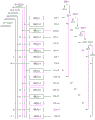
In some examples, the periods of the first clock signals are the same. When the first display frequency is adopted, the phase difference of the first clock signal loaded on the clock signal line electrically connected with the two adjacent register groups is T1/4N; t1 represents the period of the first clock signal. For example, as shown in fig. 6, when N is 2, at the first display frequency, the first clock signal ck1-1 is applied to the clock signal line ck-1, the first clock signal ck1-2 is applied to the clock signal line ck-2, the first clock signal ck1-3 is applied to the clock signal line ck-3, the first clock signal ck1-4 is applied to the clock signal line ck-4, the first clock signal ck1-5 is applied to the clock signal line ck-5, the first clock signal ck1-6 is applied to the clock signal line ck-6, the first clock signal ck1-7 is applied to the clock signal line ck-7, and the first clock signal ck1-8 is applied to the clock signal line ck-8. The shift register SR (1) -1 outputs a signal GA1-1 to the gate line GA-1, the shift register SR (1) -2 outputs a signal GA1-2 to the gate line GA-2, the shift register SR (1) -3 outputs a signal GA1-3 to the gate line GA-3, the shift register SR (1) -4 outputs a signal GA1-4 to the gate line GA-4, the shift register SR (2) -1 outputs a signal GA1-5 to the gate line GA-5, the shift register SR (2) -2 outputs a signal GA1-6 to the gate line GA-6, the shift register SR (2) -3 outputs a signal GA1-7 to the gate line GA-7, and the shift register SR (2) -4 outputs a signal GA1-8 to the gate line GA-8. The phase difference between the first clock signal ck1-1 and the first clock signal ck1-2 is T1/8, the phase difference between the first clock signal ck1-2 and the first clock signal ck1-3 is T1/8, and the phase difference between the first clock signal ck1-3 and the first clock signal ck1-4 is T1/8. For the same reason, the description is omitted here.
In some examples, the periods of the second clock signals are the same. At the second display frequency, the phase difference of the second clock signal applied to the clock signal lines electrically connected to the adjacent two cell groups is T1/2N. For example, as shown in fig. 7, when N is 2, at the second display frequency, the second clock signal ck2-1 is applied to the clock signal line ck-1, the second clock signal ck2-2 is applied to the clock signal line ck-2, the second clock signal ck2-3 is applied to the clock signal line ck-3, the second clock signal ck2-4 is applied to the clock signal line ck-4, the second clock signal ck2-5 is applied to the clock signal line ck-5, the second clock signal ck2-6 is applied to the clock signal line ck-6, the second clock signal ck2-7 is applied to the clock signal line ck-7, and the second clock signal ck2-8 is applied to the clock signal line ck-8. The shift register SR (1) -1 outputs a signal GA2-1 to the gate line GA-1, the shift register SR (1) -2 outputs a signal GA2-2 to the gate line GA-2, the shift register SR (1) -3 outputs a signal GA2-3 to the gate line GA-3, the shift register SR (1) -4 outputs a signal GA2-4 to the gate line GA-4, the shift register SR (2) -1 outputs a signal GA2-5 to the gate line GA-5, the shift register SR (2) -2 outputs a signal GA2-6 to the gate line GA-6, the shift register SR (2) -3 outputs a signal GA2-7 to the gate line GA-7, and the shift register SR (2) -4 outputs a signal GA2-8 to the gate line GA-8. The second clock signal ck2-1 is the same as the second clock signal ck2-2, the second clock signal ck2-3 is the same as the second clock signal ck2-4, the second clock signal ck2-5 is the same as the second clock signal ck2-6, and the second clock signal ck2-7 is the same as the second clock signal ck 2-8. Also, the phase difference between the second clock signal ck2-1 and the second clock signal ck2-3 is T1/4, the phase difference between the second clock signal ck2-3 and the second clock signal ck2-5 is T1/4, and the phase difference between the second clock signal ck2-5 and the second clock signal ck2-7 is T1/4. For the same reason, the description is omitted here.
In some examples, the period of the first clock signal and the period of the second clock signal are the same. Illustratively, as shown in FIG. 6 and FIG. 7, the first clock signal ck1-1 and the second clock signal ck2-1 have the same period. For the same reason, the description is omitted here.
In some examples, for a bank of cells, the timing of a second clock signal loaded by the bank of cells at the second display frequency is the same as the timing of a first clock signal loaded by a first register bank sequentially appearing in the bank of cells at the first display frequency. Illustratively, as shown in FIGS. 6 and 7, the timing of the second clock signals ck2-1 and ck2-2 is the same as the timing of the first clock signal ck 1-1. The timing of the second clock signal ck2-3 and ck2-4 is the same as the timing of the first clock signal ck 1-3. The timing of the second clock signals ck2-5 and ck2-6 is the same as the timing of the first clock signal ck 1-5. The timing of the second clock signals ck2-7 and ck2-8 is the same as the timing of the first clock signal ck 1-7.
In some examples, the second display frequency is M times the first display frequency; wherein M >1 and M is an integer. Illustratively, M may be 2, the first display frequency may be 60Hz, and correspondingly, the second display frequency is 2 times 60Hz, for example, may be 120 Hz. Of course, the first display frequency may be other frequencies such as 30Hz and 120Hz, and is not limited herein. In the following, the first display frequency is 60Hz, and the corresponding second display frequency is 120 Hz.
When the first display frequency is 60Hz, as shown in fig. 6, the first clock signal ck1-1 is applied to the clock signal line ck-1, the first clock signal ck1-2 is applied to the clock signal line ck-2, the first clock signal ck1-3 is applied to the clock signal line ck-3, the first clock signal ck1-4 is applied to the clock signal line ck-4, the first clock signal ck1-5 is applied to the clock signal line ck-5, the first clock signal ck1-6 is applied to the clock signal line ck-6, the first clock signal ck1-7 is applied to the clock signal line ck-7, and the first clock signal ck1-8 is applied to the clock signal line ck-8. The phase difference between the first clock signal ck1-1 and the first clock signal ck1-2 is T1/8, the phase difference between the first clock signal ck1-2 and the first clock signal ck1-3 is T1/8, and the phase difference between the first clock signal ck1-3 and the first clock signal ck1-4 is T1/8. The phase difference between the first clock signal ck1-4 and the first clock signal ck1-5 is T1/8. The phase difference between the first clock signal ck1-5 and the first clock signal ck1-6 is T1/8. The phase difference between the first clock signal ck1-6 and the first clock signal ck1-7 is T1/8. The phase difference between the first clock signal ck1-7 and the first clock signal ck1-8 is T1/8.
The shift register in operation of the gate driver circuit 100 operates sequentially, and the shift register SR (1) -1 outputs a signal GA1-1 to the gate line GA-1, the shift register SR (1) -2 outputs a signal GA1-2 to the gate line GA-2, the shift register SR (1) -3 outputs a signal GA1-3 to the gate line GA-3, the shift register SR (1) -4 outputs a signal GA1-4 to the gate line GA-4, the shift register SR (2) -1 outputs a signal GA1-5 to the gate line GA-5, the shift register SR (2) -2 outputs a signal GA1-6 to the gate line GA-6, the shift register SR (2) -3 outputs a signal GA1-7 to the gate line GA-7, and the shift register SR (2) -4 outputs a signal GA1-8 to the gate line GA-8. For the same reason, the description is omitted here. This enables all gate lines to be scan-driven line by line. And when each grid line is driven in a scanning way, corresponding display signals are loaded to the data lines DA, so that the display panel displays one picture.
When the second display frequency is 120Hz, as shown in fig. 7, the second clock signal ck2-1 is applied to the clock signal line ck-1, the second clock signal ck2-2 is applied to the clock signal line ck-2, the second clock signal ck2-3 is applied to the clock signal line ck-3, the second clock signal ck2-4 is applied to the clock signal line ck-4, the second clock signal ck2-5 is applied to the clock signal line ck-5, the second clock signal ck2-6 is applied to the clock signal line ck-6, the second clock signal ck2-7 is applied to the clock signal line ck-7, and the second clock signal ck2-8 is applied to the clock signal line ck-8. The second clock signal ck2-1 is the same as the second clock signal ck2-2, the second clock signal ck2-3 is the same as the second clock signal ck2-4, the second clock signal ck2-5 is the same as the second clock signal ck2-6, and the second clock signal ck2-7 is the same as the second clock signal ck 2-8. Also, the phase difference between the second clock signal ck2-1 and the second clock signal ck2-3 is T1/4, the phase difference between the second clock signal ck2-3 and the second clock signal ck2-5 is T1/4, and the phase difference between the second clock signal ck2-5 and the second clock signal ck2-7 is T1/4.
The shift register in operation of the gate driver circuit 100 is operable to output a signal GA2-1 from the shift register SR (1) -1 to the gate line GA-1, a signal GA2-2 from the shift register SR (1) -2 to the gate line GA-2, a signal GA2-3 from the shift register SR (1) -3 to the gate line GA-3, a signal GA2-4 from the shift register SR (1) -4 to the gate line GA-4, a signal GA2-5 from the shift register SR (2) -1 to the gate line GA-5, a signal GA2-6 from the shift register SR (2) -2 to the gate line GA-6, a signal GA2-7 from the shift register SR (2) -3 to the gate line GA-7, and a signal GA2-8 from the shift register SR (2) -4 to the gate line GA-8. For the same reason, the description is omitted here. This enables two adjacent gate lines to be scan-driven simultaneously. And when each grid line is driven in a scanning way, corresponding display signals are loaded to the data lines DA, so that the display panel displays one picture. When two adjacent grid lines are driven to scan simultaneously, the voltages of two data signals loaded on the same data line are the same. The voltages of the data signals that can be applied to different data lines may be different or the same, and are not limited herein.
The disclosed embodiments also provide a driving circuit of a display panel configured to:
at a first display frequency, different first clock signals are loaded to the 4N clock signal lines within one frame of scanning time, and the plurality of shift registers in the gate driving circuit 100 are controlled to sequentially operate, so that each shift register outputs different signals to drive the gate lines line by line;
loading the same second clock signal to each clock signal line electrically connected with the same unit group and loading different second clock signals to the clock signal lines electrically connected with different unit groups within one frame of scanning time at a second display frequency, so that the shift registers in different unit groups output different signals to the electrically connected grid lines, and the adjacent shift registers simultaneously drive at least two adjacent grid lines; wherein, the second display frequency is the frequency increase of the first display frequency;
the display panel comprises a plurality of grid lines, a grid driving circuit 100 electrically connected with the grid lines and 4N clock signal lines electrically connected with the grid driving circuit 100; the gate driving circuit 100 includes a plurality of shift registers arranged along an extending direction of the clock signal line, each shift register being electrically connected to one gate line correspondingly; wherein N is a positive integer;
the plurality of shift registers are divided into 4N register groups, one register group is electrically connected with the same clock signal line, the clock signal lines electrically connected with different register groups are different, and 4N-1 shift registers are arranged between adjacent shift registers in the same register group at intervals;
the 4N register groups are divided into a plurality of unit groups, one unit group comprises 2K adjacent register groups, and the register groups in different unit groups are different; wherein K is more than or equal to 1 and less than or equal to N, and K is an integer.
It should be noted that the driver circuit may take the form of an entirely hardware embodiment, an entirely software embodiment, or an embodiment combining software and hardware aspects. Moreover, the working process of the driving circuit can refer to the working process of the driving method, which is not described herein again.
The embodiment of the disclosure also provides a display device, which comprises a display panel and a driving circuit electrically connected with the display panel; the display panel includes a plurality of gate lines, a gate driving circuit 100 electrically connected to each gate line, and 4N clock signal lines electrically connected to the gate driving circuit 100; the gate driving circuit 100 includes a plurality of shift registers arranged along an extending direction of the clock signal line, each shift register being electrically connected to one gate line correspondingly; wherein N is a positive integer; the plurality of shift registers are divided into 4N register groups, one register group is electrically connected with the same clock signal line, the clock signal lines electrically connected with different register groups are different, and 4N-1 shift registers are arranged between adjacent shift registers in the same register group at intervals; the 4N register groups are divided into a plurality of unit groups, each unit group comprises 2K adjacent register groups, and the register groups in different unit groups are different; wherein K is more than or equal to 1 and less than or equal to N, and K is an integer. The structure of the display panel can be referred to the above description, and is not described herein.
And a drive circuit configured to:
at a first display frequency, different first clock signals are loaded to the 4N clock signal lines within one frame of scanning time, and the plurality of shift registers in the gate driving circuit 100 are controlled to sequentially operate, so that each shift register outputs different signals to drive the gate lines line by line;
loading the same second clock signal to each clock signal line electrically connected with the same unit group and loading different second clock signals to the clock signal lines electrically connected with different unit groups within one frame of scanning time at a second display frequency, so that the shift registers in different unit groups output different signals to the electrically connected grid lines, and the adjacent shift registers simultaneously drive at least two adjacent grid lines; the second display frequency is the frequency increase of the first display frequency.
In some examples, the display device may be: any product or component with a display function, such as a mobile phone, a tablet computer, a television, a display, a notebook computer, a digital photo frame, a navigator and the like. Other essential components of the display device are understood by those skilled in the art, and are not described herein nor should they be construed as limiting the present disclosure.
It will be apparent to those skilled in the art that various changes and modifications can be made in the present disclosure without departing from the spirit and scope of the disclosure. Thus, if such modifications and variations of the present disclosure fall within the scope of the claims of the present disclosure and their equivalents, the present disclosure is intended to include such modifications and variations as well.