CN113112949B - Gate driving circuit, display panel, display device and driving method - Google Patents
Gate driving circuit, display panel, display device and driving method Download PDFInfo
- Publication number
- CN113112949B CN113112949B CN202110460065.4A CN202110460065A CN113112949B CN 113112949 B CN113112949 B CN 113112949B CN 202110460065 A CN202110460065 A CN 202110460065A CN 113112949 B CN113112949 B CN 113112949B
- Authority
- CN
- China
- Prior art keywords
- control line
- clock control
- electrically connected
- voltage
- terminal
- Prior art date
- Legal status (The legal status is an assumption and is not a legal conclusion. Google has not performed a legal analysis and makes no representation as to the accuracy of the status listed.)
- Active
Links
Images


Classifications
-
- G—PHYSICS
- G09—EDUCATION; CRYPTOGRAPHY; DISPLAY; ADVERTISING; SEALS
- G09G—ARRANGEMENTS OR CIRCUITS FOR CONTROL OF INDICATING DEVICES USING STATIC MEANS TO PRESENT VARIABLE INFORMATION
- G09G3/00—Control arrangements or circuits, of interest only in connection with visual indicators other than cathode-ray tubes
- G09G3/20—Control arrangements or circuits, of interest only in connection with visual indicators other than cathode-ray tubes for presentation of an assembly of a number of characters, e.g. a page, by composing the assembly by combination of individual elements arranged in a matrix no fixed position being assigned to or needed to be assigned to the individual characters or partial characters
- G09G3/22—Control arrangements or circuits, of interest only in connection with visual indicators other than cathode-ray tubes for presentation of an assembly of a number of characters, e.g. a page, by composing the assembly by combination of individual elements arranged in a matrix no fixed position being assigned to or needed to be assigned to the individual characters or partial characters using controlled light sources
- G09G3/30—Control arrangements or circuits, of interest only in connection with visual indicators other than cathode-ray tubes for presentation of an assembly of a number of characters, e.g. a page, by composing the assembly by combination of individual elements arranged in a matrix no fixed position being assigned to or needed to be assigned to the individual characters or partial characters using controlled light sources using electroluminescent panels
- G09G3/32—Control arrangements or circuits, of interest only in connection with visual indicators other than cathode-ray tubes for presentation of an assembly of a number of characters, e.g. a page, by composing the assembly by combination of individual elements arranged in a matrix no fixed position being assigned to or needed to be assigned to the individual characters or partial characters using controlled light sources using electroluminescent panels semiconductive, e.g. using light-emitting diodes [LED]
- G09G3/3208—Control arrangements or circuits, of interest only in connection with visual indicators other than cathode-ray tubes for presentation of an assembly of a number of characters, e.g. a page, by composing the assembly by combination of individual elements arranged in a matrix no fixed position being assigned to or needed to be assigned to the individual characters or partial characters using controlled light sources using electroluminescent panels semiconductive, e.g. using light-emitting diodes [LED] organic, e.g. using organic light-emitting diodes [OLED]
- G09G3/3266—Details of drivers for scan electrodes
-
- G—PHYSICS
- G09—EDUCATION; CRYPTOGRAPHY; DISPLAY; ADVERTISING; SEALS
- G09G—ARRANGEMENTS OR CIRCUITS FOR CONTROL OF INDICATING DEVICES USING STATIC MEANS TO PRESENT VARIABLE INFORMATION
- G09G3/00—Control arrangements or circuits, of interest only in connection with visual indicators other than cathode-ray tubes
- G09G3/20—Control arrangements or circuits, of interest only in connection with visual indicators other than cathode-ray tubes for presentation of an assembly of a number of characters, e.g. a page, by composing the assembly by combination of individual elements arranged in a matrix no fixed position being assigned to or needed to be assigned to the individual characters or partial characters
-
- G—PHYSICS
- G11—INFORMATION STORAGE
- G11C—STATIC STORES
- G11C19/00—Digital stores in which the information is moved stepwise, e.g. shift registers
- G11C19/28—Digital stores in which the information is moved stepwise, e.g. shift registers using semiconductor elements
-
- G—PHYSICS
- G09—EDUCATION; CRYPTOGRAPHY; DISPLAY; ADVERTISING; SEALS
- G09G—ARRANGEMENTS OR CIRCUITS FOR CONTROL OF INDICATING DEVICES USING STATIC MEANS TO PRESENT VARIABLE INFORMATION
- G09G2300/00—Aspects of the constitution of display devices
- G09G2300/08—Active matrix structure, i.e. with use of active elements, inclusive of non-linear two terminal elements, in the pixels together with light emitting or modulating elements
- G09G2300/0809—Several active elements per pixel in active matrix panels
- G09G2300/0842—Several active elements per pixel in active matrix panels forming a memory circuit, e.g. a dynamic memory with one capacitor
- G09G2300/0861—Several active elements per pixel in active matrix panels forming a memory circuit, e.g. a dynamic memory with one capacitor with additional control of the display period without amending the charge stored in a pixel memory, e.g. by means of additional select electrodes
-
- G—PHYSICS
- G09—EDUCATION; CRYPTOGRAPHY; DISPLAY; ADVERTISING; SEALS
- G09G—ARRANGEMENTS OR CIRCUITS FOR CONTROL OF INDICATING DEVICES USING STATIC MEANS TO PRESENT VARIABLE INFORMATION
- G09G2310/00—Command of the display device
- G09G2310/02—Addressing, scanning or driving the display screen or processing steps related thereto
- G09G2310/0264—Details of driving circuits
- G09G2310/0283—Arrangement of drivers for different directions of scanning
-
- G—PHYSICS
- G09—EDUCATION; CRYPTOGRAPHY; DISPLAY; ADVERTISING; SEALS
- G09G—ARRANGEMENTS OR CIRCUITS FOR CONTROL OF INDICATING DEVICES USING STATIC MEANS TO PRESENT VARIABLE INFORMATION
- G09G2310/00—Command of the display device
- G09G2310/02—Addressing, scanning or driving the display screen or processing steps related thereto
- G09G2310/0264—Details of driving circuits
- G09G2310/0286—Details of a shift registers arranged for use in a driving circuit
-
- G—PHYSICS
- G09—EDUCATION; CRYPTOGRAPHY; DISPLAY; ADVERTISING; SEALS
- G09G—ARRANGEMENTS OR CIRCUITS FOR CONTROL OF INDICATING DEVICES USING STATIC MEANS TO PRESENT VARIABLE INFORMATION
- G09G2310/00—Command of the display device
- G09G2310/08—Details of timing specific for flat panels, other than clock recovery
-
- G—PHYSICS
- G09—EDUCATION; CRYPTOGRAPHY; DISPLAY; ADVERTISING; SEALS
- G09G—ARRANGEMENTS OR CIRCUITS FOR CONTROL OF INDICATING DEVICES USING STATIC MEANS TO PRESENT VARIABLE INFORMATION
- G09G2330/00—Aspects of power supply; Aspects of display protection and defect management
- G09G2330/02—Details of power systems and of start or stop of display operation
- G09G2330/028—Generation of voltages supplied to electrode drivers in a matrix display other than LCD
-
- G—PHYSICS
- G09—EDUCATION; CRYPTOGRAPHY; DISPLAY; ADVERTISING; SEALS
- G09G—ARRANGEMENTS OR CIRCUITS FOR CONTROL OF INDICATING DEVICES USING STATIC MEANS TO PRESENT VARIABLE INFORMATION
- G09G3/00—Control arrangements or circuits, of interest only in connection with visual indicators other than cathode-ray tubes
- G09G3/20—Control arrangements or circuits, of interest only in connection with visual indicators other than cathode-ray tubes for presentation of an assembly of a number of characters, e.g. a page, by composing the assembly by combination of individual elements arranged in a matrix no fixed position being assigned to or needed to be assigned to the individual characters or partial characters
- G09G3/22—Control arrangements or circuits, of interest only in connection with visual indicators other than cathode-ray tubes for presentation of an assembly of a number of characters, e.g. a page, by composing the assembly by combination of individual elements arranged in a matrix no fixed position being assigned to or needed to be assigned to the individual characters or partial characters using controlled light sources
- G09G3/30—Control arrangements or circuits, of interest only in connection with visual indicators other than cathode-ray tubes for presentation of an assembly of a number of characters, e.g. a page, by composing the assembly by combination of individual elements arranged in a matrix no fixed position being assigned to or needed to be assigned to the individual characters or partial characters using controlled light sources using electroluminescent panels
- G09G3/32—Control arrangements or circuits, of interest only in connection with visual indicators other than cathode-ray tubes for presentation of an assembly of a number of characters, e.g. a page, by composing the assembly by combination of individual elements arranged in a matrix no fixed position being assigned to or needed to be assigned to the individual characters or partial characters using controlled light sources using electroluminescent panels semiconductive, e.g. using light-emitting diodes [LED]
- G09G3/3208—Control arrangements or circuits, of interest only in connection with visual indicators other than cathode-ray tubes for presentation of an assembly of a number of characters, e.g. a page, by composing the assembly by combination of individual elements arranged in a matrix no fixed position being assigned to or needed to be assigned to the individual characters or partial characters using controlled light sources using electroluminescent panels semiconductive, e.g. using light-emitting diodes [LED] organic, e.g. using organic light-emitting diodes [OLED]
- G09G3/3225—Control arrangements or circuits, of interest only in connection with visual indicators other than cathode-ray tubes for presentation of an assembly of a number of characters, e.g. a page, by composing the assembly by combination of individual elements arranged in a matrix no fixed position being assigned to or needed to be assigned to the individual characters or partial characters using controlled light sources using electroluminescent panels semiconductive, e.g. using light-emitting diodes [LED] organic, e.g. using organic light-emitting diodes [OLED] using an active matrix
- G09G3/3233—Control arrangements or circuits, of interest only in connection with visual indicators other than cathode-ray tubes for presentation of an assembly of a number of characters, e.g. a page, by composing the assembly by combination of individual elements arranged in a matrix no fixed position being assigned to or needed to be assigned to the individual characters or partial characters using controlled light sources using electroluminescent panels semiconductive, e.g. using light-emitting diodes [LED] organic, e.g. using organic light-emitting diodes [OLED] using an active matrix with pixel circuitry controlling the current through the light-emitting element
-
- Y—GENERAL TAGGING OF NEW TECHNOLOGICAL DEVELOPMENTS; GENERAL TAGGING OF CROSS-SECTIONAL TECHNOLOGIES SPANNING OVER SEVERAL SECTIONS OF THE IPC; TECHNICAL SUBJECTS COVERED BY FORMER USPC CROSS-REFERENCE ART COLLECTIONS [XRACs] AND DIGESTS
- Y02—TECHNOLOGIES OR APPLICATIONS FOR MITIGATION OR ADAPTATION AGAINST CLIMATE CHANGE
- Y02B—CLIMATE CHANGE MITIGATION TECHNOLOGIES RELATED TO BUILDINGS, e.g. HOUSING, HOUSE APPLIANCES OR RELATED END-USER APPLICATIONS
- Y02B70/00—Technologies for an efficient end-user side electric power management and consumption
- Y02B70/10—Technologies improving the efficiency by using switched-mode power supplies [SMPS], i.e. efficient power electronics conversion e.g. power factor correction or reduction of losses in power supplies or efficient standby modes
Landscapes
- Engineering & Computer Science (AREA)
- Physics & Mathematics (AREA)
- Computer Hardware Design (AREA)
- General Physics & Mathematics (AREA)
- Theoretical Computer Science (AREA)
- Control Of Indicators Other Than Cathode Ray Tubes (AREA)
- Shift Register Type Memory (AREA)
- Liquid Crystal Display Device Control (AREA)
Abstract
本发明提供一种栅极驱动电路、显示面板、显示装置及驱动方法,栅极驱动电路包括多个级联的移位寄存器,移位寄存器包括输入单元、节点控制单元、第一输出单元和第二输出单元;输入单元的第一端与信号输入端电连接,控制端与第一信号端电连接,第二端与第一节点电连接;节点控制单元的第一端与第一节点电连接,第二端与第一信号端电连接,第三端与第一电源电压端电连接,第四端与第二电源电压端电连接,第一控制端与第一节点电连接,第二控制端与第二信号端电连接,第五端与第二节点电连接;本发明实施例以实现一个移位寄存器输出两个控制信号,从而减少栅极驱动电路中移位寄存器的数量,减小显示面板以及显示装置的边框。

The present invention provides a gate drive circuit, a display panel, a display device and a drive method. The gate drive circuit includes a plurality of cascaded shift registers, and the shift register includes an input unit, a node control unit, a first output unit and a second output unit. Two output units; the first end of the input unit is electrically connected to the signal input end, the control end is electrically connected to the first signal end, and the second end is electrically connected to the first node; the first end of the node control unit is electrically connected to the first node , the second end is electrically connected to the first signal end, the third end is electrically connected to the first power supply voltage end, the fourth end is electrically connected to the second power supply voltage end, the first control end is electrically connected to the first node, and the second control end terminal is electrically connected to the second signal terminal, and the fifth terminal is electrically connected to the second node; in the embodiment of the present invention, one shift register outputs two control signals, thereby reducing the number of shift registers in the gate drive circuit and reducing A frame of a display panel and a display device.
Description
技术领域technical field
本发明涉及显示技术领域,尤其涉及一种栅极驱动电路、显示面板、显示装置及驱动方法。The present invention relates to the field of display technology, in particular to a gate drive circuit, a display panel, a display device and a driving method.
背景技术Background technique
显示面板通常包括显示区和非显示区,显示区设置有多个像素驱动电路和发光元件,像素驱动电路用于驱动发光元件发光,以显示图像;非显示区设置有栅极驱动电路,用于为像素驱动电路提供控制信号,以使发光元件在像素驱动电路的驱动下逐行点亮。The display panel usually includes a display area and a non-display area. The display area is provided with a plurality of pixel drive circuits and light-emitting elements, and the pixel drive circuit is used to drive the light-emitting elements to emit light to display images; the non-display area is provided with a gate drive circuit for A control signal is provided for the pixel driving circuit, so that the light-emitting elements are illuminated row by row under the driving of the pixel driving circuit.
因此,栅极驱动电路一直以来都是显示领域的一大研究热点。Therefore, the gate drive circuit has always been a research hotspot in the field of display.
发明内容Contents of the invention
本发明提供一种栅极驱动电路、显示面板、显示装置及驱动方法,以实现一个移位寄存器输出两个控制信号,从而减少栅极驱动电路中移位寄存器的数量,减小显示面板以及显示装置的边框。The invention provides a gate driving circuit, a display panel, a display device and a driving method, so as to realize that one shift register outputs two control signals, thereby reducing the number of shift registers in the gate driving circuit, reducing the size of the display panel and display The border of the device.
第一方面,本发明实施例提供一种栅极驱动电路,包括多个级联的移位寄存器,所述移位寄存器包括输入单元、节点控制单元、第一输出单元和第二输出单元;In the first aspect, an embodiment of the present invention provides a gate drive circuit, including a plurality of cascaded shift registers, where the shift register includes an input unit, a node control unit, a first output unit, and a second output unit;
所述输入单元的第一端与信号输入端电连接,控制端与第一信号端电连接,第二端与第一节点电连接,被配置为根据所述第一信号端的电压以及所述信号输入端的电压控制第一节点的电压;The first terminal of the input unit is electrically connected to the signal input terminal, the control terminal is electrically connected to the first signal terminal, and the second terminal is electrically connected to the first node, and is configured to be based on the voltage of the first signal terminal and the signal the voltage at the input terminal controls the voltage at the first node;
所述节点控制单元的第一端与所述第一节点电连接,第二端与所述第一信号端电连接,第三端与第一电源电压端电连接,第四端与第二电源电压端电连接,第一控制端与所述第一节点电连接,第二控制端与第二信号端电连接,第五端与第二节点电连接,被配置为根据所述第一节点的电压、所述第一信号端的电压、所述第一电源电压端的电压、所述第二电源电压端的电压以及所述第二信号端的电压控制所述第二节点的电压;The first terminal of the node control unit is electrically connected to the first node, the second terminal is electrically connected to the first signal terminal, the third terminal is electrically connected to the first power supply voltage terminal, and the fourth terminal is electrically connected to the second power supply The voltage terminal is electrically connected, the first control terminal is electrically connected to the first node, the second control terminal is electrically connected to the second signal terminal, and the fifth terminal is electrically connected to the second node, configured to voltage, the voltage of the first signal terminal, the voltage of the first power supply voltage terminal, the voltage of the second power supply voltage terminal and the voltage of the second signal terminal control the voltage of the second node;
所述第一输出单元的第一端与所述第二电源电压端电连接,第二端与第三信号端电连接,第三端与第一输出端电连接,第一控制端与所述第二节点电连接,第二控制端与所述第一节点电连接,被配置根据所述第二电源电压端的电压、所述第三信号端的电压、所述第一节点的电压以及所述第二节点的电压,控制所述第一输出端的电压;The first terminal of the first output unit is electrically connected to the second power supply voltage terminal, the second terminal is electrically connected to the third signal terminal, the third terminal is electrically connected to the first output terminal, and the first control terminal is electrically connected to the The second node is electrically connected, the second control terminal is electrically connected to the first node, and configured according to the voltage of the second power supply voltage terminal, the voltage of the third signal terminal, the voltage of the first node, and the first node. The voltage of the two nodes controls the voltage of the first output terminal;
所述第二输出单元的第一端与所述第二电源电压端电连接,第二端与第四信号端电连接,第三端与第二输出端电连接,第一控制端与所述第二节点电连接,第二控制端与所述第一节点电连接,被配置根据所述第二电源电压端的电压、所述第四信号端的电压、所述第一节点的电压以及所述第二节点的电压,控制所述第二输出端的电压。The first terminal of the second output unit is electrically connected to the second power supply voltage terminal, the second terminal is electrically connected to the fourth signal terminal, the third terminal is electrically connected to the second output terminal, and the first control terminal is electrically connected to the The second node is electrically connected, the second control terminal is electrically connected to the first node, and configured according to the voltage of the second power supply voltage terminal, the voltage of the fourth signal terminal, the voltage of the first node, and the first node. The voltage of the second node controls the voltage of the second output terminal.
第二方面,本发明实施例提供一种显示面板,包括第一方面所述的栅极驱动电路。In a second aspect, an embodiment of the present invention provides a display panel, including the gate driving circuit described in the first aspect.
第三方面,本发明实施例提供一种显示装置,包括第二方面所述的显示面板。In a third aspect, an embodiment of the present invention provides a display device, including the display panel described in the second aspect.
第四方面,本发明实施例提供一种第一方面所述栅极驱动电路的驱动方法,包括:In a fourth aspect, an embodiment of the present invention provides a method for driving the gate drive circuit described in the first aspect, including:
在输入阶段,向信号输入端施加导通电压,向第一信号端施加导通电压,向第二信号端施加截止电压,输入单元响应于所述第一信号端的导通电压,将所述信号输入端的导通电压传递至第一节点;In the input stage, a conduction voltage is applied to the signal input terminal, a conduction voltage is applied to the first signal terminal, and a cut-off voltage is applied to the second signal terminal, and the input unit responds to the conduction voltage of the first signal terminal, and the signal passing the turn-on voltage of the input terminal to the first node;
在第一输出阶段,向所述第一信号端施加截止电压,向所述第二信号端施加截止电压,向第三信号端施加导通电压,向第四信号端施加截止电压,节点控制单元的第一控制端响应于所述第一节点的导通电压,将所述第一信号端的截止电压传递至第二节点,所述第一输出单元的第二控制端响应于所述第一节点保持的所述导通电压,将所述第三信号端的导通电压传递至第一输出端;In the first output stage, a cut-off voltage is applied to the first signal terminal, a cut-off voltage is applied to the second signal terminal, a conduction voltage is applied to the third signal terminal, and a cut-off voltage is applied to the fourth signal terminal, the node control unit The first control end of the first output unit responds to the turn-on voltage of the first node, and transmits the cut-off voltage of the first signal end to the second node, and the second control end of the first output unit responds to the first node maintaining the conduction voltage, passing the conduction voltage of the third signal terminal to the first output terminal;
在第二输出阶段,向所述第一信号端施加截止电压,向所述第二信号端施加截止电压,向所述第三信号端施加截止电压,向所述第四信号端施加导通电压,所述节点控制单元的第一控制端响应于所述第一节点的导通电压,将所述第一信号端的截止电压传递至所述第二节点,所述第二输出单元的第二控制端响应于所述第一节点保持的所述导通电压,将所述第四信号端的导通电压传递至第二输出端;In the second output stage, a cut-off voltage is applied to the first signal terminal, a cut-off voltage is applied to the second signal terminal, a cut-off voltage is applied to the third signal terminal, and a turn-on voltage is applied to the fourth signal terminal , the first control terminal of the node control unit transmits the cut-off voltage of the first signal terminal to the second node in response to the turn-on voltage of the first node, and the second control terminal of the second output unit The terminal transmits the conduction voltage of the fourth signal terminal to the second output terminal in response to the conduction voltage held by the first node;
在维持阶段,向所述第一信号端施加截止电压,向所述第二信号端施加导通电压,所述节点控制单元的第二控制端响应于所述所述第二信号端的导通电压,将第一电源电压端输入的电压传递至所述第二节点,将第二电源电压端输入的电压传递至第一节点,所述第一输出端和所述第二输出端输出非有效电平。In the maintenance phase, a cut-off voltage is applied to the first signal terminal, a conduction voltage is applied to the second signal terminal, and the second control terminal of the node control unit responds to the conduction voltage of the second signal terminal , the voltage input from the first power supply voltage terminal is transmitted to the second node, the voltage input from the second power supply voltage terminal is transmitted to the first node, and the first output terminal and the second output terminal output a non-effective voltage flat.
本发明实施例提供一种栅极驱动电路,在输入阶段,通过输入单元将导通电压传递至第一节点。在第一输出阶段,通过节点控制单元控制第二节点的电压,第一输出单元响应于第一节点、第二节点的电压,将第三信号端的导通电压传递至第一输出端。在第二输出阶段,通过节点控制单元控制第二节点的电压,第二输出单元响应于第一节点、第二节点的电压,将第四信号端的导通电压传递至第二输出端。由于栅极驱动电路的第一输出端和第二输出端可以分别输出控制信号,故而一个移位寄存器可以输出两个控制信号,从而减少栅极驱动电路中移位寄存器的数量,减小显示面板以及显示装置的边框。An embodiment of the present invention provides a gate driving circuit. In an input phase, the conduction voltage is transmitted to the first node through the input unit. In the first output stage, the voltage of the second node is controlled by the node control unit, and the first output unit transmits the conduction voltage of the third signal terminal to the first output terminal in response to the voltages of the first node and the second node. In the second output stage, the voltage of the second node is controlled by the node control unit, and the second output unit transmits the conduction voltage of the fourth signal terminal to the second output terminal in response to the voltages of the first node and the second node. Since the first output terminal and the second output terminal of the gate drive circuit can respectively output control signals, one shift register can output two control signals, thereby reducing the number of shift registers in the gate drive circuit and reducing the size of the display panel. and the frame of the display device.
附图说明Description of drawings
图1为本发明实施例提供的一种栅极驱动电路的结构示意图;FIG. 1 is a schematic structural diagram of a gate drive circuit provided by an embodiment of the present invention;
图2为本发明实施例提供的一种移位寄存器的电路示意图;2 is a schematic circuit diagram of a shift register provided by an embodiment of the present invention;
图3为本发明实施例提供的另一种移位寄存器的电路示意图;FIG. 3 is a schematic circuit diagram of another shift register provided by an embodiment of the present invention;
图4为本发明实施例提供的另一种移位寄存器的电路示意图;FIG. 4 is a schematic circuit diagram of another shift register provided by an embodiment of the present invention;
图5为本发明实施例提供的另一种移位寄存器的电路示意图;FIG. 5 is a schematic circuit diagram of another shift register provided by an embodiment of the present invention;
图6为本发明实施例提供的另一种栅极驱动电路的结构示意图;FIG. 6 is a schematic structural diagram of another gate drive circuit provided by an embodiment of the present invention;
图7为本发明实施例提供的另一种栅极驱动电路的结构示意图;FIG. 7 is a schematic structural diagram of another gate drive circuit provided by an embodiment of the present invention;
图8为本发明实施例提供的另一种栅极驱动电路的结构示意图;FIG. 8 is a schematic structural diagram of another gate drive circuit provided by an embodiment of the present invention;
图9为本发明实施例提供的另一种移位寄存器的电路示意图;FIG. 9 is a schematic circuit diagram of another shift register provided by an embodiment of the present invention;
图10为本发明实施例提供的另一种栅极驱动电路的结构示意图;FIG. 10 is a schematic structural diagram of another gate drive circuit provided by an embodiment of the present invention;
图11为本发明实施例提供的另一种栅极驱动电路的结构示意图;FIG. 11 is a schematic structural diagram of another gate drive circuit provided by an embodiment of the present invention;
图12为本发明实施例提供的另一种栅极驱动电路的结构示意图;FIG. 12 is a schematic structural diagram of another gate drive circuit provided by an embodiment of the present invention;
图13为本发明实施例提供的另一种栅极驱动电路的结构示意图;FIG. 13 is a schematic structural diagram of another gate drive circuit provided by an embodiment of the present invention;
图14为本发明实施例提供的一种显示面板的结构示意图;FIG. 14 is a schematic structural diagram of a display panel provided by an embodiment of the present invention;
图15为本发明实施例提供的一种像素驱动电路的电路示意图;FIG. 15 is a schematic circuit diagram of a pixel driving circuit provided by an embodiment of the present invention;
图16为本发明实施例提供的另一种显示面板的结构示意图;FIG. 16 is a schematic structural diagram of another display panel provided by an embodiment of the present invention;
图17为本发明实施例提供的一种显示装置的结构示意图;FIG. 17 is a schematic structural diagram of a display device provided by an embodiment of the present invention;
图18为本发明实施例提供的一种栅极驱动电路的驱动方法流程图;FIG. 18 is a flowchart of a driving method of a gate driving circuit provided by an embodiment of the present invention;
图19为本发明实施例提供的一种栅极驱动电路的驱动时序图;FIG. 19 is a driving timing diagram of a gate driving circuit provided by an embodiment of the present invention;
图20为栅极驱动电路在输入阶段的示意图;20 is a schematic diagram of the gate drive circuit in the input stage;
图21为栅极驱动电路在第一输出阶段的示意图;21 is a schematic diagram of the gate drive circuit in the first output stage;
图22为栅极驱动电路在第二输出阶段的示意图;22 is a schematic diagram of the gate drive circuit in the second output stage;
图23为栅极驱动电路在维持阶段的示意图;23 is a schematic diagram of the gate drive circuit in the maintenance phase;
图24为本发明实施例提供的另一种栅极驱动电路的驱动时序图;FIG. 24 is a driving timing diagram of another gate driving circuit provided by an embodiment of the present invention;
图25为本发明实施例提供的另一种栅极驱动电路的驱动时序图;FIG. 25 is a driving timing diagram of another gate driving circuit provided by an embodiment of the present invention;
图26为本发明实施例提供的另一种栅极驱动电路的驱动时序图;FIG. 26 is a driving timing diagram of another gate driving circuit provided by an embodiment of the present invention;
图27为本发明实施例提供的另一种栅极驱动电路的驱动时序图;FIG. 27 is a driving timing diagram of another gate driving circuit provided by an embodiment of the present invention;
图28为本发明实施例提供的另一种栅极驱动电路的驱动时序图;FIG. 28 is a driving timing diagram of another gate driving circuit provided by an embodiment of the present invention;
图29为本发明实施例提供的另一种栅极驱动电路的驱动时序图。FIG. 29 is a driving timing diagram of another gate driving circuit provided by an embodiment of the present invention.
具体实施方式Detailed ways
下面结合附图和实施例对本发明作进一步的详细说明。可以理解的是,此处所描述的具体实施例仅仅用于解释本发明,而非对本发明的限定。另外还需要说明的是,为了便于描述,附图中仅示出了与本发明相关的部分而非全部结构。The present invention will be further described in detail below in conjunction with the accompanying drawings and embodiments. It should be understood that the specific embodiments described here are only used to explain the present invention, but not to limit the present invention. In addition, it should be noted that, for the convenience of description, only some structures related to the present invention are shown in the drawings but not all structures.
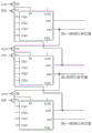
图1为本发明实施例提供的一种栅极驱动电路的结构示意图,图2为本发明实施例提供的一种移位寄存器的电路示意图,参考图1和图2,栅极驱动电路包括多个级联的移位寄存器VSR,移位寄存器VSR包括输入单元10、节点控制单元20、第一输出单元40和第二输出单元50。其中,输入单元10的第一端与信号输入端IN电连接,输入单元10的控制端与第一信号端CK1电连接,输入单元10的第二端与第一节点N1电连接,输入单元10被配置为根据第一信号端CK1的电压以及信号输入端IN的电压控制第一节点N1的电压。节点控制单元20的第一端与第一节点N1电连接,节点控制单元20的第二端与第一信号端CK1电连接,节点控制单元20的第三端与第一电源电压端VGL电连接,节点控制单元20的第四端与第二电源电压端VGH电连接,节点控制单元20的第一控制端与第一节点N1电连接,节点控制单元20的第二控制端与第二信号端CK2电连接,节点控制单元20的第五端与第二节点N2电连接,节点控制单元20被配置为根据第一节点N1的电压、第一信号端CK1的电压、第一电源电压端VGL的电压、第二电源电压端VGH的电压以及第二信号端CK2的电压控制第二节点N2的电压。第一输出单元40的第一端与第二电源电压端VGH电连接,第一输出单元40的第二端与第三信号端CK3电连接,第一输出单元40的第三端与第一输出端out1电连接,第一输出单元40的第一控制端与第二节点N2电连接,第一输出单元40的第二控制端与第一节点N1电连接,第一输出单元40被配置根据第二电源电压端VGH的电压、第三信号端CK3的电压、第一节点N1的电压以及第二节点N2的电压,控制第一输出端out1的电压。第二输出单元50的第一端与第二电源电压端VGH电连接,第二输出单元50的第二端与第四信号端CK4电连接,第二输出单元50的第三端与第二输出端out2电连接,第二输出单元50的第一控制端与第二节点N2电连接,第二输出单元50的第二控制端与第一节点N1电连接,第二输出单元50被配置根据第二电源电压端VGH的电压、第四信号端CK4的电压、第一节点N1的电压以及第二节点N2的电压,控制第二输出端out2的电压。Figure 1 is a schematic structural diagram of a gate drive circuit provided by an embodiment of the present invention, and Figure 2 is a schematic circuit diagram of a shift register provided by an embodiment of the present invention, referring to Figures 1 and 2, the gate drive circuit includes multiple A cascaded shift register VSR, the shift register VSR includes an
本发明实施例提供一种栅极驱动电路,在输入阶段,通过输入单元10将导通电压传递至第一节点N1。在第一输出阶段,通过节点控制单元20控制第二节点N2的电压,第一输出单元40响应于第一节点N1、第二节点N2的电压,将第三信号端CK3的导通电压传递至第一输出端out1。在第二输出阶段,通过节点控制单元20控制第二节点N2的电压,第二输出单元50响应于第一节点N1、第二节点N2的电压,将第四信号端CK4的导通电压传递至第二输出端out2。由于栅极驱动电路的第一输出端out1和第二输出端out2可以分别输出控制信号,故而一个移位寄存器VSR可以输出两个控制信号,从而减少栅极驱动电路中移位寄存器VSR的数量,减小显示面板以及显示装置的边框。An embodiment of the present invention provides a gate driving circuit. In an input phase, the conduction voltage is transmitted to the first node N1 through the
需要说明的是,在一实施方式中,第一节点N1和第二节点N2可以为实际的连接点。在另一实施方式中,第一节点N1和第二节点N2也可以为虚拟的连接点。总之,第一节点N1、输入单元10的第二端、节点控制单元20的第一端以及节点控制单元20的第一控制端同电位,第二节点N2、节点控制单元20的第五端、第一输出单元40的第一控制端以及第二输出单元50的第一控制端同电位。It should be noted that, in an implementation manner, the first node N1 and the second node N2 may be actual connection points. In another implementation manner, the first node N1 and the second node N2 may also be virtual connection points. In short, the first node N1, the second terminal of the
可选地,参考图2,栅极驱动电路还可以包括存储单元30,存储单元30的第一端与第二电源电压端VGH电连接,存储单元30的第二端与第二节点N2电连接。存储单元30被配置为存储第二节点N2的电位。Optionally, referring to FIG. 2, the gate drive circuit may further include a
图3为本发明实施例提供的另一种移位寄存器的电路示意图,参考图3,输入单元10包括第一晶体管T1,第一晶体管T1的栅极与第一信号端CK1电连接,第一晶体管T1的第一极与信号输入端IN电连接,第一晶体管T1的第二极与第一节点N1电连接。也就是说,第一晶体管T1的第二极与节点控制单元20的第一端电连接。FIG. 3 is a schematic circuit diagram of another shift register provided by an embodiment of the present invention. Referring to FIG. 3 , the
可选地,参考图3,节点控制单元20包括第二晶体管T2、第三晶体管T3和第四晶体管T4。第二晶体管T2的栅极与第一节点N1电连接,第二晶体管T2的第一极与第一信号端CK1电连接,第二晶体管T2的第二极与第二节点N2电连接。也就是说,第二晶体管T2的第二极与第一输出单元40的第一控制端电连接。第三晶体管T3的栅极与第二信号端CK2电连接,第三晶体管T3的第一极与第一节点N1电连接,第三晶体管T3的第二极与第二电源电压端VGH电连接。第四晶体管T4的栅极与第二信号端CK2电连接,第四晶体管T4的第一极与第一电源电压端VGL电连接,第四晶体管T4的第二极与第二节点N2电连接。Optionally, referring to FIG. 3 , the
可选地,参考图3,存储单元30包括第一电容C1,第一电容C1的第一极板与第二电源电压端VGH电连接,第一电容C1的第二极板与第二节点N2电连接。也就是说,第一电容C1的第二极板与第一输出单元40的第一控制端电连接。Optionally, referring to FIG. 3 , the
可选地,参考图3,第一输出单元40包括第五晶体管T5和第六晶体管T6。第五晶体管T5的栅极与第二节点N2电连接,也就是说,第五晶体管T5的栅极与节点控制单元20的第五端电连接。第五晶体管T5的第一极与第二电源电压端VGH电连接,第五晶体管T5的第二极与第一输出端out1电连接。第六晶体管T6的栅极与第一节点N1电连接,也就是说,第六晶体管T6的栅极与输入单元10的第二端电连接。第六晶体管T6的第一极与第一输出端out1电连接,第六晶体管T6的第二极与第三信号端CK3电连接。第二输出单元50包括第七晶体管T7和第八晶体管T8。第七晶体管T7的栅极与第二节点N2电连接,也就是说,第七晶体管T7的栅极与节点控制单元20的第五端电连接。第七晶体管T7的第一极与第二电源电压端VGH电连接,第七晶体管T7的第二极与第二输出端out2电连接。第八晶体管T8的栅极与第一节点N1电连接,也就是说,第八晶体管T8的栅极与输入单元10的第二端电连接。第八晶体管T8的第一极与第二输出端out2电连接,第八晶体管T8的第二极与第四信号端CK4电连接。Optionally, referring to FIG. 3 , the
图4为本发明实施例提供的另一种移位寄存器的电路示意图,参考图4,第一输出单元40还包括第二电容C2,第二电容C2的第一极板与第一节点N1电连接,即,第二电容C2的第一极板与第六晶体管T6的栅极电连接。第二电容C2的第二极板与第一输出端out1电连接,即第二电容C2的第二极板与第六晶体管T6的第一极电连接,从而第二电容C2串接于第六晶体管T6的栅极与第六晶体管T6的第一极之间,起到自举作用。第二输出单元50还包括第三电容C3,第三电容C3的第一极板与第一节点N1电连接,即,第三电容C3的第一极板与第八晶体管T8的栅极电连接。第三电容C3的第二极板与第二输出端out2电连接,即第三电容C3的第二极板与第八晶体管T8的第一极电连接,从而第三电容C3串接于第八晶体管T8的栅极与第八晶体管T8的第一极之间,起到自举作用。FIG. 4 is a schematic circuit diagram of another shift register provided by an embodiment of the present invention. Referring to FIG. 4 , the
图5为本发明实施例提供的另一种移位寄存器的电路示意图,参考图5,栅极驱动电路还包括第九晶体管T9,第九晶体管T9的栅极与第一电源电压端VGL电连接,第九晶体管T9的第一极与第一节点N1电连接,第九晶体管T9的第二极与第一输出单元40的第二控制端以及第二输出单元50的第二控制端电连接。本发明实施例中,第九晶体管T9的栅极与第一电源电压端VGL电连接,第九晶体管T9始终处于导通状态,第一节点N1控制第一输出单元40的第二控制端以及第二输出单元50的第二控制端。设置第九晶体管T9的优点在于,第一节点N1的电压过低时,第九晶体管T9处于截止状态,从而可以防止将过低的电压施加到第一输出单元40的第二控制端以及第二输出单元50的第二控制端。FIG. 5 is a schematic circuit diagram of another shift register provided by an embodiment of the present invention. Referring to FIG. 5 , the gate drive circuit further includes a ninth transistor T9, the gate of the ninth transistor T9 is electrically connected to the first power supply voltage terminal VGL , the first pole of the ninth transistor T9 is electrically connected to the first node N1, and the second pole of the ninth transistor T9 is electrically connected to the second control terminal of the
示例性地,参考图3-图5,第一晶体管T1、第三晶体管T3和第四晶体管T4可以为双栅晶体管,双栅晶体管可以降低漏电流。For example, referring to FIGS. 3-5 , the first transistor T1 , the third transistor T3 and the fourth transistor T4 may be double-gate transistors, and the double-gate transistors may reduce leakage current.
图6为本发明实施例提供的另一种栅极驱动电路的结构示意图,图7为本发明实施例提供的另一种栅极驱动电路的结构示意图,参考图6和图7,栅极驱动电路还包括多条时钟控制线,移位寄存器VSR的第一信号端CK1、第二信号端CK2、第三信号端CK3和第四信号端CK4分别与四条时钟控制线电连接。本发明实施例中,同一个移位寄存器VSR的第一信号端CK1、第二信号端CK2、第三信号端CK3和第四信号端CK4分别与四条不同的时钟控制线电连接,从而可以通过四条不同的时钟控制线为同一个移位寄存器VSR的第一信号端CK1、第二信号端CK2、第三信号端CK3和第四信号端CK4分别施加电信号。FIG. 6 is a schematic structural diagram of another gate driving circuit provided by an embodiment of the present invention, and FIG. 7 is a schematic structural diagram of another gate driving circuit provided by an embodiment of the present invention. Referring to FIG. 6 and FIG. 7 , the gate driving The circuit also includes a plurality of clock control lines. The first signal terminal CK1, the second signal terminal CK2, the third signal terminal CK3 and the fourth signal terminal CK4 of the shift register VSR are respectively electrically connected to the four clock control lines. In the embodiment of the present invention, the first signal terminal CK1, the second signal terminal CK2, the third signal terminal CK3 and the fourth signal terminal CK4 of the same shift register VSR are respectively electrically connected to four different clock control lines, so that the Four different clock control lines respectively apply electrical signals to the first signal terminal CK1 , the second signal terminal CK2 , the third signal terminal CK3 and the fourth signal terminal CK4 of the same shift register VSR.
可选地,参考图6,第i级移位寄存器的信号输入端IN与第i-1级移位寄存器的第二输出端out2电连接,第i+1级移位寄存器的信号输入端IN与第i级移位寄存器的第二输出端out2电连接。其中,i为大于1的正整数。Optionally, referring to FIG. 6, the signal input terminal IN of the i-th stage shift register is electrically connected to the second output terminal out2 of the i-1-th stage shift register, and the signal input terminal IN of the i+1-th stage shift register It is electrically connected with the second output terminal out2 of the i-th stage shift register. Wherein, i is a positive integer greater than 1.
示例性地,第2级移位寄存器的信号输入端IN与第1级移位寄存器的第二输出端out2电连接,第3级移位寄存器的信号输入端IN与第2级移位寄存器的第二输出端out2电连接,依次类推。Exemplarily, the signal input end IN of the second-stage shift register is electrically connected to the second output end out2 of the first-stage shift register, and the signal input end IN of the third-stage shift register is connected to the second output end of the second-stage shift register. The second output terminal out2 is electrically connected, and so on.
可选地,参考图7,栅极驱动电路包括依次级联的第一移位寄存器VSR1、第二移位寄存器VSR2和第三移位寄存器VSR3。由于第一移位寄存器VSR1、第二移位寄存器VSR2和第三移位寄存器VSR3依次级联,因此第二移位寄存器VSR2的信号输入端IN与第一移位寄存器VSR1的第二输出端out2电连接,第三移位寄存器VSR3的信号输入端IN与第二移位寄存器VSR2的第二输出端out2电连接。多条时钟控制线包括第一时钟控制线CLK1、第二时钟控制线CLK2、第三时钟控制线CLK3、第四时钟控制线CLK4、第五时钟控制线CLK5、第六时钟控制线CLK6和第七时钟控制线CLK7。第一移位寄存器VSR1的第一信号端CK1与第五时钟控制线CLK5电连接,第一移位寄存器VSR1的第二信号端CK2与第七时钟控制线CLK7电连接,第一移位寄存器VSR1的第三信号端CK3与第一时钟控制线CLK1电连接,第一移位寄存器VSR1的第四信号端CK4与第二时钟控制线CLK2电连接。第二移位寄存器VSR2的第一信号端CK1与第六时钟控制线CLK6电连接,第二移位寄存器VSR2的第二信号端CK2与第五时钟控制线CLK5电连接,第二移位寄存器VSR2的第三信号端CK3与第三时钟控制线CLK3电连接,第二移位寄存器VSR2的第四信号端CK4与第四时钟控制线CLK4电连接。第三移位寄存器VSR3的第一信号端CK1与第七时钟控制线CLK7电连接,第三移位寄存器VSR3的第二信号端CK2与第六时钟控制线CLK6电连接,第三移位寄存器VSR3的第三信号端CK3与第一时钟控制线CLK1电连接,第三移位寄存器VSR3的第四信号端CK4与第二时钟控制线CLK2电连接。Optionally, referring to FIG. 7 , the gate drive circuit includes a first shift register VSR1 , a second shift register VSR2 and a third shift register VSR3 cascaded in sequence. Since the first shift register VSR1, the second shift register VSR2 and the third shift register VSR3 are sequentially cascaded, the signal input terminal IN of the second shift register VSR2 is connected to the second output terminal out2 of the first shift register VSR1 The signal input terminal IN of the third shift register VSR3 is electrically connected with the second output terminal out2 of the second shift register VSR2. Multiple clock control lines include first clock control line CLK1, second clock control line CLK2, third clock control line CLK3, fourth clock control line CLK4, fifth clock control line CLK5, sixth clock control line CLK6 and seventh clock control line Clock control line CLK7. The first signal terminal CK1 of the first shift register VSR1 is electrically connected to the fifth clock control line CLK5, the second signal terminal CK2 of the first shift register VSR1 is electrically connected to the seventh clock control line CLK7, and the first shift register VSR1 The third signal terminal CK3 of the first shift register VSR1 is electrically connected to the first clock control line CLK1, and the fourth signal terminal CK4 of the first shift register VSR1 is electrically connected to the second clock control line CLK2. The first signal end CK1 of the second shift register VSR2 is electrically connected to the sixth clock control line CLK6, the second signal end CK2 of the second shift register VSR2 is electrically connected to the fifth clock control line CLK5, and the second shift register VSR2 The third signal terminal CK3 of the second shift register VSR2 is electrically connected to the third clock control line CLK3, and the fourth signal terminal CK4 of the second shift register VSR2 is electrically connected to the fourth clock control line CLK4. The first signal terminal CK1 of the third shift register VSR3 is electrically connected to the seventh clock control line CLK7, the second signal terminal CK2 of the third shift register VSR3 is electrically connected to the sixth clock control line CLK6, and the third shift register VSR3 The third signal terminal CK3 of the third shift register VSR3 is electrically connected to the first clock control line CLK1, and the fourth signal terminal CK4 of the third shift register VSR3 is electrically connected to the second clock control line CLK2.
示例性地,参考图7,第1级移位寄存器可以为第一移位寄存器VSR1,第2级移位寄存器可以为第二移位寄存器VSR2,第3级移位寄存器可以为第三移位寄存器VSR3。进一步地,第4级移位寄存器可以为第一移位寄存器VSR1,第5级移位寄存器可以为第二移位寄存器VSR2,第6级移位寄存器可以为第三移位寄存器VSR3,依次类推。则,第一移位寄存器VSR1的信号输入端IN可以与第三移位寄存器VSR3的第二输出端out2电连接。Exemplarily, referring to FIG. 7, the shift register of the first stage may be the first shift register VSR1, the shift register of the second stage may be the second shift register VSR2, and the shift register of the third stage may be the third shift register. Register VSR3. Further, the 4th stage shift register can be the first shift register VSR1, the 5th stage shift register can be the second shift register VSR2, the 6th stage shift register can be the third shift register VSR3, and so on . Then, the signal input terminal IN of the first shift register VSR1 can be electrically connected with the second output terminal out2 of the third shift register VSR3.
图8为本发明实施例提供的另一种栅极驱动电路的结构示意图,参考图8,栅极驱动电路包括依次级联的第一移位寄存器VSR1和第二移位寄存器VSR2,由于第一移位寄存器VSR1和第二移位寄存器VSR2依次级联,因此第二移位寄存器VSR2的信号输入端IN与第一移位寄存器VSR1的第二输出端out2电连接。多条时钟控制线包括第一时钟控制线CLK1、第二时钟控制线CLK2、第三时钟控制线CLK3和第四时钟控制线CLK4。第一移位寄存器VSR1的第一信号端CK1与第四时钟控制线CLK4电连接,第一移位寄存器VSR1的第二信号端CK2与第三时钟控制线CLK3电连接,第一移位寄存器VSR1的第三信号端CK3与第一时钟控制线CLK1电连接,第一移位寄存器VSR1的第四信号端CK4与第二时钟控制线CLK2电连接。第二移位寄存器VSR2的第一信号端CK1与第二时钟控制线CLK2电连接,第二移位寄存器VSR2的第二信号端CK2与第一时钟控制线CLK1电连接,第二移位寄存器VSR2的第三信号端CK3与第三时钟控制线CLK3电连接,第二移位寄存器VSR2的第四信号端CK4与第四时钟控制线CLK4电连接。FIG. 8 is a schematic structural diagram of another gate drive circuit provided by an embodiment of the present invention. Referring to FIG. 8, the gate drive circuit includes a first shift register VSR1 and a second shift register VSR2 cascaded in sequence. The shift register VSR1 and the second shift register VSR2 are cascaded in sequence, so the signal input terminal IN of the second shift register VSR2 is electrically connected to the second output terminal out2 of the first shift register VSR1 . The plurality of clock control lines include a first clock control line CLK1, a second clock control line CLK2, a third clock control line CLK3, and a fourth clock control line CLK4. The first signal terminal CK1 of the first shift register VSR1 is electrically connected to the fourth clock control line CLK4, the second signal terminal CK2 of the first shift register VSR1 is electrically connected to the third clock control line CLK3, and the first shift register VSR1 The third signal terminal CK3 of the first shift register VSR1 is electrically connected to the first clock control line CLK1, and the fourth signal terminal CK4 of the first shift register VSR1 is electrically connected to the second clock control line CLK2. The first signal end CK1 of the second shift register VSR2 is electrically connected to the second clock control line CLK2, the second signal end CK2 of the second shift register VSR2 is electrically connected to the first clock control line CLK1, and the second shift register VSR2 The third signal terminal CK3 of the second shift register VSR2 is electrically connected to the third clock control line CLK3, and the fourth signal terminal CK4 of the second shift register VSR2 is electrically connected to the fourth clock control line CLK4.
示例性地,参考图8,第1级移位寄存器可以为第一移位寄存器VSR1,第2级移位寄存器可以为第二移位寄存器VSR2,第3级移位寄存器可以为第一移位寄存器VSR1。进一步地,第4级移位寄存器可以为第二移位寄存器VSR2,第5级移位寄存器可以为第一移位寄存器VSR1,第6级移位寄存器可以为第二移位寄存器VSR2,依次类推。则,第一移位寄存器VSR1的信号输入端IN可以与第二移位寄存器VSR2的第二输出端out2电连接。Exemplarily, referring to FIG. 8, the shift register of the first stage may be the first shift register VSR1, the shift register of the second stage may be the second shift register VSR2, and the shift register of the third stage may be the first shift register VSR2. Register VSR1. Further, the 4th stage shift register can be the second shift register VSR2, the 5th stage shift register can be the first shift register VSR1, the 6th stage shift register can be the second shift register VSR2, and so on . Then, the signal input terminal IN of the first shift register VSR1 can be electrically connected to the second output terminal out2 of the second shift register VSR2.
图9为本发明实施例提供的另一种移位寄存器的电路示意图,参考图9,移位寄存器VSR还包括正反控制单元60,正反控制单元60包括第十晶体管T10和第十一晶体管T11。第十晶体管T10的栅极与第一正反信号端U2D电连接,第十一晶体管T11的栅极与第二正反信号端D2U电连接,第十晶体管T10的第一极以及第十一晶体管T11的第一极均与信号输入端IN电连接。也就是说,第十晶体管T10的第一极与输入单元10的第一端电连接,第十一晶体管T11的第一极与输入单元10的第一端电连接。本发明实施例中,移位寄存器VSR还包括正反控制单元60,从而提供一种具有正反向扫描功能的栅极驱动电路,来实现正向显示和反向显示。FIG. 9 is a schematic circuit diagram of another shift register provided by an embodiment of the present invention. Referring to FIG. 9, the shift register VSR also includes a forward and reverse
图10为本发明实施例提供的另一种栅极驱动电路的结构示意图,参考图10,第i级移位寄存器中第十晶体管T10的第二极与第i-1级移位寄存器的第一输出端out1电连接。第i-1级移位寄存器中第十一晶体管T11的第二极与第i级移位寄存器的第二输出端out2电连接。第i+1级移位寄存器中第十晶体管T10的第二极与第i级移位寄存器的第一输出端out1电连接。第i级移位寄存器中第十一晶体管T11的第二极与第i+1级移位寄存器的第二输出端out2电连接。其中,i为大于1的正整数。FIG. 10 is a schematic structural diagram of another gate drive circuit provided by an embodiment of the present invention. Referring to FIG. 10 , the second pole of the tenth transistor T10 in the i-th stage shift register is connected to the An output terminal out1 is electrically connected. The second pole of the eleventh transistor T11 in the i-1th stage shift register is electrically connected to the second output terminal out2 of the i-th stage shift register. The second pole of the tenth transistor T10 in the (i+1)th stage shift register is electrically connected to the first output terminal out1 of the i-th stage shift register. The second pole of the eleventh transistor T11 in the i-th shift register is electrically connected to the second output terminal out2 of the i+1-th shift register. Wherein, i is a positive integer greater than 1.
示例性地,第2级移位寄存器中第十晶体管T10的第二极与第1级移位寄存器的第一输出端out1电连接。第1级移位寄存器中第十一晶体管T11的第二极与第2级移位寄存器的第二输出端out2电连接。第3级移位寄存器中第十晶体管T10的第二极与第2级移位寄存器的第一输出端out1电连接。第2级移位寄存器中第十一晶体管T11的第二极与第3级移位寄存器的第二输出端out2电连接,依次类推。Exemplarily, the second pole of the tenth transistor T10 in the second-stage shift register is electrically connected to the first output terminal out1 of the first-stage shift register. The second pole of the eleventh transistor T11 in the first-stage shift register is electrically connected to the second output terminal out2 of the second-stage shift register. The second pole of the tenth transistor T10 in the third-stage shift register is electrically connected to the first output terminal out1 of the second-stage shift register. The second pole of the eleventh transistor T11 in the second-stage shift register is electrically connected to the second output terminal out2 of the third-stage shift register, and so on.
图11为本发明实施例提供的另一种栅极驱动电路的结构示意图,参考图10和图11,栅极驱动电路包括依次级联的第一移位寄存器VSR1、第二移位寄存器VSR2、第三移位寄存器VSR3和第四移位寄存器VSR4。由于第一移位寄存器VSR1、第二移位寄存器VSR2、第三移位寄存器VSR3和第四移位寄存器VSR4依次级联,因此,第二移位寄存器VSR2中第十晶体管T10的第二极与第一移位寄存器VSR1的第一输出端out1电连接。第一移位寄存器VSR1中第十一晶体管T11的第二极与第二移位寄存器VSR2的第二输出端out2电连接。第三移位寄存器VSR3中第十晶体管T10的第二极与第二移位寄存器VSR2的第一输出端out1电连接。第二移位寄存器VSR2中第十一晶体管T11的第二极与第三移位寄存器VSR3的第二输出端out2电连接。第四移位寄存器VSR4中第十晶体管T10的第二极与第三移位寄存器VSR3的第一输出端out1电连接。第三移位寄存器VSR3中第十一晶体管T11的第二极与第四移位寄存器VSR4的第二输出端out2电连接。多条时钟控制线包括第一时钟控制线CLK1、第二时钟控制线CLK2、第三时钟控制线CLK3、第四时钟控制线CLK4、第五时钟控制线CLK5、第六时钟控制线CLK6、第七时钟控制线CLK7和第八时钟控制线CLK8。第一移位寄存器VSR1的第一信号端CK1与第四时钟控制线CLK4电连接,第一移位寄存器VSR1的第二信号端CK2与第三时钟控制线CLK3电连接,第一移位寄存器VSR1的第三信号端CK3与第一时钟控制线CLK1电连接,第一移位寄存器VSR1的第四信号端CK4与第二时钟控制线CLK2电连接。第二移位寄存器VSR2的第一信号端CK1与第七时钟控制线CLK7电连接,第二移位寄存器VSR2的第二信号端CK2与第六时钟控制线CLK6电连接,第二移位寄存器VSR2的第三信号端CK3与第八时钟控制线CLK8电连接,第二移位寄存器VSR2的第四信号端CK4与第五时钟控制线CLK5电连接。第三移位寄存器VSR3的第一信号端CK1与第二时钟控制线CLK2电连接,第三移位寄存器VSR3的第二信号端CK2与第一时钟控制线CLK1电连接,第三移位寄存器VSR3的第三信号端CK3与第三时钟控制线CLK3电连接,第三移位寄存器VSR3的第四信号端CK4与第四时钟控制线CLK4电连接。第四移位寄存器VSR4的第一信号端CK1与第五时钟控制线CLK5电连接,第四移位寄存器VSR4的第二信号端CK2与第八时钟控制线CLK8电连接,第四移位寄存器VSR4的第三信号端CK3与第六时钟控制线CLK6电连接,第四移位寄存器VSR4的第四信号端CK4与第七时钟控制线CLK7电连接。Fig. 11 is a schematic structural diagram of another gate driving circuit provided by an embodiment of the present invention. Referring to Fig. 10 and Fig. 11 , the gate driving circuit includes sequentially cascaded first shift register VSR1, second shift register VSR2, The third shift register VSR3 and the fourth shift register VSR4. Since the first shift register VSR1, the second shift register VSR2, the third shift register VSR3 and the fourth shift register VSR4 are sequentially cascaded, therefore, the second pole of the tenth transistor T10 in the second shift register VSR2 and The first output terminal out1 of the first shift register VSR1 is electrically connected. The second pole of the eleventh transistor T11 in the first shift register VSR1 is electrically connected to the second output terminal out2 of the second shift register VSR2. The second pole of the tenth transistor T10 in the third shift register VSR3 is electrically connected to the first output terminal out1 of the second shift register VSR2. The second pole of the eleventh transistor T11 in the second shift register VSR2 is electrically connected to the second output terminal out2 of the third shift register VSR3. The second pole of the tenth transistor T10 in the fourth shift register VSR4 is electrically connected to the first output terminal out1 of the third shift register VSR3. The second pole of the eleventh transistor T11 in the third shift register VSR3 is electrically connected to the second output terminal out2 of the fourth shift register VSR4. Multiple clock control lines include first clock control line CLK1, second clock control line CLK2, third clock control line CLK3, fourth clock control line CLK4, fifth clock control line CLK5, sixth clock control line CLK6, seventh clock control line A clock control line CLK7 and an eighth clock control line CLK8. The first signal terminal CK1 of the first shift register VSR1 is electrically connected to the fourth clock control line CLK4, the second signal terminal CK2 of the first shift register VSR1 is electrically connected to the third clock control line CLK3, and the first shift register VSR1 The third signal terminal CK3 of the first shift register VSR1 is electrically connected to the first clock control line CLK1, and the fourth signal terminal CK4 of the first shift register VSR1 is electrically connected to the second clock control line CLK2. The first signal end CK1 of the second shift register VSR2 is electrically connected to the seventh clock control line CLK7, the second signal end CK2 of the second shift register VSR2 is electrically connected to the sixth clock control line CLK6, and the second shift register VSR2 The third signal terminal CK3 of the second shift register VSR2 is electrically connected to the eighth clock control line CLK8, and the fourth signal terminal CK4 of the second shift register VSR2 is electrically connected to the fifth clock control line CLK5. The first signal end CK1 of the third shift register VSR3 is electrically connected to the second clock control line CLK2, the second signal end CK2 of the third shift register VSR3 is electrically connected to the first clock control line CLK1, and the third shift register VSR3 The third signal terminal CK3 of the third shift register VSR3 is electrically connected to the third clock control line CLK3, and the fourth signal terminal CK4 of the third shift register VSR3 is electrically connected to the fourth clock control line CLK4. The first signal end CK1 of the fourth shift register VSR4 is electrically connected to the fifth clock control line CLK5, the second signal end CK2 of the fourth shift register VSR4 is electrically connected to the eighth clock control line CLK8, and the fourth shift register VSR4 The third signal terminal CK3 of the fourth shift register VSR4 is electrically connected to the sixth clock control line CLK6, and the fourth signal terminal CK4 of the fourth shift register VSR4 is electrically connected to the seventh clock control line CLK7.
示例性地,参考图11,第1级移位寄存器可以为第一移位寄存器VSR1,第2级移位寄存器可以为第二移位寄存器VSR2,第3级移位寄存器可以为第三移位寄存器VSR3,第4级移位寄存器可以为第四移位寄存器VSR4。进一步地,第5级移位寄存器可以为第一移位寄存器VSR1,第6级移位寄存器可以为第二移位寄存器VSR2,第7级移位寄存器可以为第三移位寄存器VSR3,第8级移位寄存器可以为第四移位寄存器VSR4,依次类推。则,第一移位寄存器VSR1中第十晶体管T10的第二极与第四移位寄存器VSR4的第一输出端out1电连接。第四移位寄存器VSR4中第十一晶体管T11的第二极与第一移位寄存器VSR1的第二输出端out2电连接。Exemplarily, referring to FIG. 11 , the shift register of the first stage can be the first shift register VSR1, the shift register of the second stage can be the second shift register VSR2, and the shift register of the third stage can be the third shift register. The register VSR3, the 4th stage shift register may be the fourth shift register VSR4. Further, the shift register of the 5th stage can be the first shift register VSR1, the shift register of the 6th stage can be the second shift register VSR2, the shift register of the 7th stage can be the third shift register VSR3, and the shift register of the 8th stage can be the third shift register VSR3. The stage shift register can be the fourth shift register VSR4, and so on. Then, the second pole of the tenth transistor T10 in the first shift register VSR1 is electrically connected to the first output terminal out1 of the fourth shift register VSR4. The second pole of the eleventh transistor T11 in the fourth shift register VSR4 is electrically connected to the second output terminal out2 of the first shift register VSR1 .
图12为本发明实施例提供的另一种栅极驱动电路的结构示意图,参考图12,第i级移位寄存器中第十晶体管T10的第二极与第i-1级移位寄存器的第二输出端out2电连接,第i-1级移位寄存器中第十一晶体管T11的第二极与第i级移位寄存器的第一输出端out1电连接。第i+1级移位寄存器中第十晶体管T10的第二极与第i级移位寄存器的第二输出端out2电连接,第i级移位寄存器中第十一晶体管T11的第二极与第i+1级移位寄存器的第一输出端out1电连接。其中,i为大于1的正整数。FIG. 12 is a schematic structural diagram of another gate drive circuit provided by an embodiment of the present invention. Referring to FIG. 12 , the second pole of the tenth transistor T10 in the i-th stage shift register is connected to the The two output terminals out2 are electrically connected, and the second pole of the eleventh transistor T11 in the i-1th stage shift register is electrically connected to the first output terminal out1 of the i-th stage shift register. The second pole of the tenth transistor T10 in the i+1 shift register is electrically connected to the second output terminal out2 of the i shift register, and the second pole of the eleventh transistor T11 in the i shift register is connected to The first output terminal out1 of the i+1th stage shift register is electrically connected. Wherein, i is a positive integer greater than 1.
示例性地,第2级移位寄存器中第十晶体管T10的第二极与第1级移位寄存器的第二输出端out2电连接,第1级移位寄存器中第十一晶体管T11的第二极与第2级移位寄存器的第一输出端out1电连接。第3级移位寄存器中第十晶体管T10的第二极与第2级移位寄存器的第二输出端out2电连接,第2级移位寄存器中第十一晶体管T11的第二极与第3级移位寄存器的第一输出端out1电连接。依次类推。Exemplarily, the second pole of the tenth transistor T10 in the second-stage shift register is electrically connected to the second output terminal out2 of the first-stage shift register, and the second pole of the eleventh transistor T11 in the first-stage shift register The pole is electrically connected to the first output terminal out1 of the second-stage shift register. The second pole of the tenth transistor T10 in the third-stage shift register is electrically connected to the second output terminal out2 of the second-stage shift register, and the second pole of the eleventh transistor T11 in the second-stage shift register is connected to the second pole of the third-stage shift register. The first output terminal out1 of the stage shift register is electrically connected. And so on.
图13为本发明实施例提供的另一种栅极驱动电路的结构示意图,参考图12和图13,栅极驱动电路包括依次级联的第一移位寄存器VSR1和第二移位寄存器VSR2,由于第一移位寄存器VSR1和第二移位寄存器VSR2依次级联,因此,第二移位寄存器VSR2中第十晶体管T10的第二极与第一移位寄存器VSR1的第二输出端out2电连接,第1级移位寄存器中第十一晶体管T11的第二极与第2级移位寄存器的第一输出端out1电连接。多条时钟控制线包括第一时钟控制线CLK1、第二时钟控制线CLK2、第三时钟控制线CLK3、第四时钟控制线CLK4、第五时钟控制线CLK5、第六时钟控制线CLK6、第七时钟控制线CLK7和第八时钟控制线CLK8。第一移位寄存器VSR1的第一信号端CK1与第四时钟控制线CLK4电连接,第一移位寄存器VSR1的第二信号端CK2与第三时钟控制线CLK3电连接,第一移位寄存器VSR1的第三信号端CK3与第五时钟控制线CLK5电连接,第一移位寄存器VSR1的第四信号端CK4与第六时钟控制线CLK6电连接。第二移位寄存器VSR2的第一信号端CK1与第二时钟控制线CLK2电连接,第二移位寄存器VSR2的第二信号端CK2与第一时钟控制线CLK1电连接,第二移位寄存器VSR2的第三信号端CK3与第七时钟控制线CLK7电连接,第二移位寄存器VSR2的第四信号端CK4与第八时钟控制线CLK8电连接。FIG. 13 is a schematic structural diagram of another gate drive circuit provided by an embodiment of the present invention. Referring to FIG. 12 and FIG. 13 , the gate drive circuit includes a first shift register VSR1 and a second shift register VSR2 cascaded in sequence, Since the first shift register VSR1 and the second shift register VSR2 are sequentially cascaded, the second pole of the tenth transistor T10 in the second shift register VSR2 is electrically connected to the second output terminal out2 of the first shift register VSR1 , the second pole of the eleventh transistor T11 in the first-stage shift register is electrically connected to the first output terminal out1 of the second-stage shift register. Multiple clock control lines include first clock control line CLK1, second clock control line CLK2, third clock control line CLK3, fourth clock control line CLK4, fifth clock control line CLK5, sixth clock control line CLK6, seventh clock control line A clock control line CLK7 and an eighth clock control line CLK8. The first signal terminal CK1 of the first shift register VSR1 is electrically connected to the fourth clock control line CLK4, the second signal terminal CK2 of the first shift register VSR1 is electrically connected to the third clock control line CLK3, and the first shift register VSR1 The third signal terminal CK3 of the first shift register VSR1 is electrically connected to the fifth clock control line CLK5, and the fourth signal terminal CK4 of the first shift register VSR1 is electrically connected to the sixth clock control line CLK6. The first signal end CK1 of the second shift register VSR2 is electrically connected to the second clock control line CLK2, the second signal end CK2 of the second shift register VSR2 is electrically connected to the first clock control line CLK1, and the second shift register VSR2 The third signal terminal CK3 of the second shift register VSR2 is electrically connected to the seventh clock control line CLK7, and the fourth signal terminal CK4 of the second shift register VSR2 is electrically connected to the eighth clock control line CLK8.
示例性地,参考图13,第1级移位寄存器可以为第一移位寄存器VSR1,第2级移位寄存器可以为第二移位寄存器VSR2,第3级移位寄存器可以为第一移位寄存器VSR1。进一步地,第4级移位寄存器可以为第二移位寄存器VSR2。依次类推。则,第一移位寄存器VSR1中第十晶体管T10的第二极与第二移位寄存器VSR2的第二输出端out2电连接,第二移位寄存器VSR2中第十一晶体管T11的第二极与第一移位寄存器VSR1的第一输出端out1电连接。Exemplarily, referring to FIG. 13, the shift register of the first stage may be the first shift register VSR1, the shift register of the second stage may be the second shift register VSR2, and the shift register of the third stage may be the first shift register VSR2. Register VSR1. Further, the fourth stage shift register may be the second shift register VSR2. And so on. Then, the second pole of the tenth transistor T10 in the first shift register VSR1 is electrically connected to the second output terminal out2 of the second shift register VSR2, and the second pole of the eleventh transistor T11 in the second shift register VSR2 is electrically connected to the second pole of the eleventh transistor T11 in the second shift register VSR2. The first output terminal out1 of the first shift register VSR1 is electrically connected.
可选地,继续参考图5,第一电源电压端VGL提供低电平,第二电源电压端VGH提供高电平。Optionally, continuing to refer to FIG. 5 , the first power supply voltage terminal VGL provides a low level, and the second power supply voltage terminal VGH provides a high level.
可选地,继续参考图5,同一个移位寄存器VSR中,第一输出端out1与第二输出端out2顺次输出有效电平信号。在一实施方式中,同一个移位寄存器VSR的第一输出端out1先输出有效电平信号,之后,同一个移位寄存器VSR的第二输出端out2再输出有效电平信号。在另一实施方式中,同一个移位寄存器VSR的第二输出端out2先输出有效电平信号,之后,同一个移位寄存器VSR的第一输出端out1再输出有效电平信号。Optionally, continuing to refer to FIG. 5 , in the same shift register VSR, the first output terminal out1 and the second output terminal out2 sequentially output active level signals. In one embodiment, the first output terminal out1 of the same shift register VSR first outputs a valid level signal, and then the second output terminal out2 of the same shift register VSR outputs a valid level signal. In another embodiment, the second output terminal out2 of the same shift register VSR first outputs a valid level signal, and then the first output terminal out1 of the same shift register VSR outputs a valid level signal.
示例性地,继续参考图5,本发明各实施例中以P型晶体管为例,例如,第一晶体管T1、第二晶体管T2、第三晶体管T3、第四晶体管T4、第五晶体管T5、第六晶体管T6、第七晶体管T7、第八晶体管T8、第九晶体管T9均为P型晶体管。对P型晶体管而言,有效电平为低电平,非有效电平为高电平,即,P型晶体管低电平导通,高电平截止。在其他实施方式中,栅极驱动电路中晶体管还可以采用N型晶体管,此时,对N型晶体管而言,有效电平为高电平,非有效电平为低电平。Exemplarily, continuing to refer to FIG. 5, P-type transistors are taken as an example in various embodiments of the present invention, for example, the first transistor T1, the second transistor T2, the third transistor T3, the fourth transistor T4, the fifth transistor T5, the The sixth transistor T6, the seventh transistor T7, the eighth transistor T8, and the ninth transistor T9 are all P-type transistors. For a P-type transistor, the active level is a low level, and the inactive level is a high level, that is, the P-type transistor is turned on at a low level and turned off at a high level. In other implementation manners, the transistors in the gate driving circuit may also be N-type transistors. At this time, for the N-type transistors, the active level is high level, and the inactive level is low level.
图14为本发明实施例提供的一种显示面板的结构示意图,参考图14,显示面板包括上述实施例中的栅极驱动电路110。由于本发明实施例提供的显示面板包括上述实施例中的栅极驱动电路110,因此栅极驱动电路110中一个移位寄存器VSR可以输出两个控制信号,从而减少栅极驱动电路110中移位寄存器VSR的数量,减小显示面板的边框。FIG. 14 is a schematic structural diagram of a display panel provided by an embodiment of the present invention. Referring to FIG. 14 , the display panel includes the
可选地,参考图14,显示面板还包括多个阵列排布的像素驱动电路130。像素驱动电路130包括第一扫描信号端131和第二扫描信号端132(图14中以圆点突出示意第一扫描信号端131和第二扫描信号端132),第j级移位寄存器VSR的第一输出端out1与第j行像素驱动电路130的第一扫描信号端131电连接,第j级移位寄存器VSR的第二输出端out2与第j行像素驱动电路130的第二扫描信号端132电连接。其中,j为大于或者等于1的正整数。本发明实施例中,第一输出端out1与第一扫描信号端131电连接,第二输出端out2与第二扫描信号端132电连接,从而每一个移位寄存器VSR可以为一行像素驱动电路130提供控制信号。Optionally, referring to FIG. 14 , the display panel further includes a plurality of
示例性地,第1级移位寄存器VSR的第一输出端out1与第1行像素驱动电路130的第一扫描信号端131电连接,第1级移位寄存器VSR的第二输出端out2与第1行像素驱动电路130的第二扫描信号端132电连接。第2级移位寄存器VSR的第一输出端out1与第2行像素驱动电路130的第一扫描信号端131电连接,第2级移位寄存器VSR的第二输出端out2与第2行像素驱动电路130的第二扫描信号端132电连接。Exemplarily, the first output terminal out1 of the first-stage shift register VSR is electrically connected to the first
示例性地,参考图14,显示面板包括显示区AA和非显示区NAA,栅极驱动电路110位于非显示区NAA,像素驱动电路130位于显示区AA,多个像素驱动电路130沿第一方向和第二方向阵列排布。显示面板还包括多条扫描线121和多条数据线122,多条扫描线121沿第一方向延伸并沿第二方向排列。多条数据线122沿第二方向延伸并沿第一方向排列。第一输出端out1与一条扫描线121电连接,第二输出端out2与一条扫描线121电连接,每一个移位寄存器VSR与两条扫描线121电连接。Exemplarily, referring to FIG. 14 , the display panel includes a display area AA and a non-display area NAA, the
图15为本发明实施例提供的一种像素驱动电路的电路示意图,参考图14和图15,像素驱动电路130包括第一开关管M1、第二开关管M2、第三开关管M3、第四开关管M4、第五开关管M5、第六开关管M6和驱动晶体管M0,第一开关管M1的栅极与第一扫描信号端131电连接,第一开关管M1的第一极与参考电压端VREF电连接,第一开关管M1的第二极与驱动晶体管M0的栅极电连接。第二开关管M2的栅极与第二扫描信号端132电连接,第二开关管M2的第一极与数据端DATA电连接,第二开关管M2的第二极与驱动晶体管M0的第一极电连接。第三开关管M3的栅极与第二扫描信号端132电连接,第三开关管M3的第一极与驱动晶体管M0的栅极电连接,第三开关管M3的第二极与驱动晶体管M0的第二极电连接。第四开关管M4的栅极与第二扫描信号端132电连接,第四开关管M4的第一极与参考电压端VREF电连接,第四开关管M4的第二极与发光元件OLED的阳极电连接。第五开关管M5的栅极与发光控制端EMIT电连接。第五开关管M5的第一极与第一电源端PVDD电连接,第五开关管M5的第二极与驱动晶体管M0的第一极电连接。第六开关管M6的栅极与发光控制端EMIT电连接。第六开关管M6的第一极与驱动晶体管M0的第二极电连接。第六开关管M6的第一极与发光元件OLED的阳极电连接。发光元件OLED的阴极与第二电源端PVEE电连接。示例性地,第一扫描信号端131用于对像素驱动电路进行初始化控制,第二扫描信号端132用于对像素驱动电路进行补偿控制。数据端DATA与数据线122电连接,第一电源端PVDD与第二电源电压端VGH电连接,第二电源端PVEE与第一电源电压端VGL电连接。本发明实施例中,发光元件OLED为有机发光元件,显示面板为有机发光显示面板。在其他实施方式中,像素驱动电路130还可以用于驱动液晶显示面板、量子点显示面板、微发光二极管显示面板等。Fig. 15 is a schematic circuit diagram of a pixel driving circuit provided by an embodiment of the present invention. Referring to Fig. 14 and Fig. 15, the
图16为本发明实施例提供的一种显示面板的结构示意图,参考图16,显示面板还包括多个阵列排布的像素驱动电路130(图16中以圆点突出示意扫描信号端133)。像素驱动电路130包括扫描信号端133,第j级移位寄存器VSR的第一输出端out1与第2j-1行像素驱动电路130的扫描信号端133电连接,第j级移位寄存器VSR的第二输出端out2与第2j行像素驱动电路130的扫描信号端133电连接。其中,j为大于或者等于1的正整数。本发明实施例中,第一输出端out1和第二输出端out2分别与两行扫描信号端133电连接,从而每一个移位寄存器VSR可以为两行像素驱动电路130提供控制信号。FIG. 16 is a schematic structural diagram of a display panel provided by an embodiment of the present invention. Referring to FIG. 16 , the display panel further includes a plurality of
示例性地,第1级移位寄存器VSR的第一输出端out1与第1行像素驱动电路130的扫描信号端133电连接,第1级移位寄存器VSR的第二输出端out2与第2行像素驱动电路130的扫描信号端133电连接。第2级移位寄存器VSR的第一输出端out1与第3行像素驱动电路130的扫描信号端133电连接,第2级移位寄存器VSR的第二输出端out2与第4行像素驱动电路130的扫描信号端133电连接。依次类推。本发明实施例中的像素驱动电路130例如可以采用2T1C或者7T1C等本领域公知的像素驱动电路,在此不再赘述。Exemplarily, the first output terminal out1 of the first-stage shift register VSR is electrically connected to the
本发明实施例还提供了一种显示装置。图17为本发明实施例提供的一种显示装置的示意图,参考图17,显示装置包括本发明实施例提供的任意一种显示面板。显示装置具体可以为手机、平板电脑、车载显示装置以及智能可穿戴设备等。The embodiment of the present invention also provides a display device. FIG. 17 is a schematic diagram of a display device provided by an embodiment of the present invention. Referring to FIG. 17 , the display device includes any display panel provided by an embodiment of the present invention. Specifically, the display device may be a mobile phone, a tablet computer, a vehicle-mounted display device, and a smart wearable device.
图18为本发明实施例提供的一种栅极驱动电路的驱动方法流程图,图19为本发明实施例提供的一种栅极驱动电路的驱动时序图,图20为栅极驱动电路在输入阶段的示意图,图21为栅极驱动电路在第一输出阶段的示意图,图22为栅极驱动电路在第二输出阶段的示意图,图23为栅极驱动电路在维持阶段的示意图,参考图18-图23,栅极驱动电路的驱动方法包括:FIG. 18 is a flowchart of a driving method of a gate driving circuit provided by an embodiment of the present invention, FIG. 19 is a driving timing diagram of a gate driving circuit provided by an embodiment of the present invention, and FIG. 21 is a schematic diagram of the gate drive circuit in the first output stage, FIG. 22 is a schematic diagram of the gate drive circuit in the second output stage, and FIG. 23 is a schematic diagram of the gate drive circuit in the maintenance stage. Refer to FIG. 18 - Figure 23, the driving method of the gate driving circuit includes:
S101、在输入阶段,向信号输入端IN施加导通电压,向第一信号端CK1施加导通电压,向第二信号端CK2施加截止电压,输入单元10响应于第一信号端CK1的导通电压,将信号输入端IN的导通电压传递至第一节点N1。S101. In the input stage, apply a conduction voltage to the signal input terminal IN, apply a conduction voltage to the first signal terminal CK1, and apply a cut-off voltage to the second signal terminal CK2, and the
示例性地,参考图19和图20,在输入阶段,向第一信号端CK1施加低电平,从而将第一晶体管T1导通。向信号输入端IN施加低电平,信号输入端IN的低电平传递至第一节点N1,使第一节点N1为低电平。第一节点N1连接至第二晶体管T2的栅极,将第二晶体管T2导通,第一信号端CK1的低电平传递至第二节点N2。第二节点N2连接至第五晶体管T5和第七晶体管T7的栅极,将第五晶体管T5和第七晶体管T7导通,第二电源电压端VGH的高电平经过第五晶体管T5传递至第一输出端out1,第二电源电压端VGH的高电平经过第七晶体管T7传递至第二输出端out2。向第二信号端CK2施加高电平,从而将第三晶体管T3和第四晶体管T4截止。For example, referring to FIG. 19 and FIG. 20 , in the input stage, a low level is applied to the first signal terminal CK1 , so as to turn on the first transistor T1 . A low level is applied to the signal input terminal IN, and the low level of the signal input terminal IN is transmitted to the first node N1, so that the first node N1 is at a low level. The first node N1 is connected to the gate of the second transistor T2, the second transistor T2 is turned on, and the low level of the first signal terminal CK1 is transmitted to the second node N2. The second node N2 is connected to the gates of the fifth transistor T5 and the seventh transistor T7, and turns on the fifth transistor T5 and the seventh transistor T7, and the high level of the second power supply voltage terminal VGH is transmitted to the fifth transistor T5 through the fifth transistor T5. An output terminal out1, the high level of the second power supply voltage terminal VGH is transmitted to the second output terminal out2 through the seventh transistor T7. A high level is applied to the second signal terminal CK2, thereby turning off the third transistor T3 and the fourth transistor T4.
S102、在第一输出阶段,向第一信号端CK1施加截止电压,向第二信号端CK2施加截止电压,向第三信号端CK3施加导通电压,向第四信号端CK4施加截止电压,节点控制单元20的第一控制端响应于第一节点N1的导通电压,将第一信号端CK1的截止电压传递至第二节点N2,第一输出单元40的第二控制端响应于第一节点N1保持的导通电压,将第三信号端CK3的导通电压传递至第一输出端out1。S102. In the first output stage, apply a cut-off voltage to the first signal terminal CK1, apply a cut-off voltage to the second signal terminal CK2, apply a turn-on voltage to the third signal terminal CK3, and apply a cut-off voltage to the fourth signal terminal CK4, the node The first control terminal of the
示例性地,参考图19和图21,在第一输出阶段,向第一信号端CK1施加高电平,从而将第一晶体管T1截止。第一节点N1维持输入阶段的低电平,从而第一节点N1的低电平将第二晶体管T2导通。向第一信号端CK1施加的高电平经第二晶体管T2传递到第二节点N2,第二节点N2的高电平将第五晶体管T5和第七晶体管T7截止。向第二信号端CK2施加高电平,从而将第三晶体管T3和第四晶体管T4截止。第一电源电压端VGL的低电平将第九晶体管T9始终导通。第一节点N1的低电平将第六晶体管T6和第八晶体管T8导通。向第三信号端CK3施加低电平,从而第三信号端CK3的低电平经第六晶体管T6传递至第一输出端out1,第一输出端out1输出低电平信号,即有效电平。向第四信号端CK4施加高电平,第四信号端CK4的高电平经第八晶体管T8传递至第二输出端out2,第二输出端out2输出高电平信号,即非有效电平。For example, referring to FIG. 19 and FIG. 21 , in the first output stage, a high level is applied to the first signal terminal CK1 , thereby turning off the first transistor T1 . The first node N1 maintains the low level of the input phase, so the low level of the first node N1 turns on the second transistor T2. The high level applied to the first signal terminal CK1 is transmitted to the second node N2 through the second transistor T2, and the high level of the second node N2 turns off the fifth transistor T5 and the seventh transistor T7. A high level is applied to the second signal terminal CK2, thereby turning off the third transistor T3 and the fourth transistor T4. The low level of the first power supply voltage terminal VGL turns on the ninth transistor T9 all the time. The low level of the first node N1 turns on the sixth transistor T6 and the eighth transistor T8. A low level is applied to the third signal terminal CK3, so that the low level of the third signal terminal CK3 is transmitted to the first output terminal out1 through the sixth transistor T6, and the first output terminal out1 outputs a low level signal, that is, an active level. A high level is applied to the fourth signal terminal CK4, and the high level of the fourth signal terminal CK4 is transmitted to the second output terminal out2 through the eighth transistor T8, and the second output terminal out2 outputs a high level signal, that is, an inactive level.
S103、在第二输出阶段,向第一信号端CK1施加截止电压,向第二信号端CK2施加截止电压,向第三信号端CK3施加截止电压,向第四信号端CK4施加导通电压,节点控制单元20的第一控制端响应于第一节点N1的导通电压,将第一信号端CK1的截止电压传递至第二节点N2,第二输出单元50的第二控制端响应于第一节点N1保持的导通电压,将第四信号端CK4的导通电压传递至第二输出端out2。S103. In the second output stage, apply a cut-off voltage to the first signal terminal CK1, apply a cut-off voltage to the second signal terminal CK2, apply a cut-off voltage to the third signal terminal CK3, and apply a turn-on voltage to the fourth signal terminal CK4, the node The first control terminal of the
示例性地,参考图19和图22,在第二输出阶段,向第一信号端CK1施加高电平,从而将第一晶体管T1截止。第一节点N1维持输入阶段的低电平,从而第一节点N1的低电平将第二晶体管T2导通。向第一信号端CK1施加的高电平经第二晶体管T2传递到第二节点N2,第二节点N2的高电平将第五晶体管T5和第七晶体管T7截止。向第二信号端CK2施加高电平,从而将第三晶体管T3和第四晶体管T4截止。第一电源电压端VGL的低电平将第九晶体管T9始终导通。第一节点N1的低电平将第六晶体管T6和第八晶体管T8导通。向第三信号端CK3施加高电平,从而第三信号端CK3的高电平经第六晶体管T6传递至第一输出端out1,第一输出端out1输出高电平信号,即非有效电平。向第四信号端CK4施加低电平,第四信号端CK4的低电平经第八晶体管T8传递至第二输出端out2,第二输出端out2输出低电平信号,即有效电平。For example, referring to FIG. 19 and FIG. 22 , in the second output stage, a high level is applied to the first signal terminal CK1 , thereby turning off the first transistor T1 . The first node N1 maintains the low level of the input phase, so the low level of the first node N1 turns on the second transistor T2. The high level applied to the first signal terminal CK1 is transmitted to the second node N2 through the second transistor T2, and the high level of the second node N2 turns off the fifth transistor T5 and the seventh transistor T7. A high level is applied to the second signal terminal CK2, thereby turning off the third transistor T3 and the fourth transistor T4. The low level of the first power supply voltage terminal VGL turns on the ninth transistor T9 all the time. The low level of the first node N1 turns on the sixth transistor T6 and the eighth transistor T8. Apply a high level to the third signal terminal CK3, so that the high level of the third signal terminal CK3 is transmitted to the first output terminal out1 through the sixth transistor T6, and the first output terminal out1 outputs a high level signal, that is, an inactive level . A low level is applied to the fourth signal terminal CK4, and the low level of the fourth signal terminal CK4 is transmitted to the second output terminal out2 through the eighth transistor T8, and the second output terminal out2 outputs a low level signal, that is, an effective level.
S104、在维持阶段,向第一信号端CK1施加截止电压,向第二信号端CK2施加导通电压,节点控制单元20的第二控制端响应于第二信号端CK2的导通电压,将第一电源电压端VGL输入的电压传递至第二节点N2,将第二电源电压端VGH输入的电压传递至第一节点N1,第一输出端out1和第二输出端out2输出非有效电平。S104. In the maintenance phase, apply a cut-off voltage to the first signal terminal CK1, and apply a turn-on voltage to the second signal terminal CK2, and the second control terminal of the
示例性地,参考图19和图22,在维持阶段,向第一信号端CK1施加高电平,从而将第一晶体管T1截止。向第二信号端CK2施加低电平,第二信号端CK2的低电平控制第三晶体管T3和第四晶体管T4导通,从而第二电源电压端VGH的高电平传递至第一节点N1。第一电源电压端VGL的低电平将第九晶体管T9始终导通。第一节点N1的高电平将第六晶体管T6和第八晶体管T8截止。由于第二信号端CK2的低电平将第四晶体管T4导通,第一电源电压端VGL的低电平传递至第二节点N2,第二节点N2的低电平将第五晶体管T5和第七晶体管T7导通,第二电源电压端VGH的高电平经过第五晶体管T5传递至第一输出端out1,第二电源电压端VGH的高电平经过第七晶体管T7传递至第二输出端out2。For example, referring to FIG. 19 and FIG. 22 , in the sustain phase, a high level is applied to the first signal terminal CK1 , thereby turning off the first transistor T1 . A low level is applied to the second signal terminal CK2, and the low level of the second signal terminal CK2 controls the conduction of the third transistor T3 and the fourth transistor T4, so that the high level of the second power supply voltage terminal VGH is transmitted to the first node N1 . The low level of the first power supply voltage terminal VGL turns on the ninth transistor T9 all the time. The high level of the first node N1 turns off the sixth transistor T6 and the eighth transistor T8. Since the low level of the second signal terminal CK2 turns on the fourth transistor T4, the low level of the first power supply voltage terminal VGL is transmitted to the second node N2, and the low level of the second node N2 turns on the fifth transistor T5 and the second node N2. The seven transistors T7 are turned on, the high level of the second power supply voltage terminal VGH is transmitted to the first output terminal out1 through the fifth transistor T5, and the high level of the second power supply voltage terminal VGH is transmitted to the second output terminal through the seventh transistor T7 out2.
本发明实施例提供一种栅极驱动电路的驱动方法,用于驱动上述实施例中的栅极驱动电路,在输入阶段,通过输入单元10将导通电压传递至第一节点N1。在第一输出阶段,通过节点控制单元20控制第二节点N2的电压,第一输出单元40响应于第一节点N1、第二节点N2的电压,将第三信号端CK3的导通电压传递至第一输出端out1。在第二输出阶段,通过节点控制单元20控制第二节点N2的电压,第二输出单元50响应于第一节点N1、第二节点N2的电压,将第四信号端CK4的导通电压传递至第二输出端out2。由于栅极驱动电路的第一输出端out1和第二输出端out2可以分别输出控制信号,故而一个移位寄存器VSR可以输出两个控制信号,从而减少栅极驱动电路中移位寄存器VSR的数量,减小显示面板以及显示装置的边框。An embodiment of the present invention provides a driving method for a gate driving circuit, which is used to drive the gate driving circuit in the above embodiment. In the input stage, the conduction voltage is transmitted to the first node N1 through the
上述驱动方法为栅极驱动电路中一个移位寄存器的驱动方法,通常地,栅极驱动电路包括多个级联的移位寄存器,栅极驱动电路中任一移位寄存器可以采用上述的驱动方法。本发明实施例还对栅极驱动电路中多个移位寄存器级联之后的驱动方法做进一步的介绍。The above-mentioned driving method is a driving method of a shift register in the gate driving circuit. Generally, the gate driving circuit includes a plurality of cascaded shift registers, and any shift register in the gate driving circuit can adopt the above-mentioned driving method . The embodiment of the present invention further introduces the driving method after multiple shift registers are cascaded in the gate driving circuit.
图24为本发明实施例提供的另一种栅极驱动电路的驱动时序图,图24所示驱动时序用于驱动如图7所示栅极驱动电路,参考图7和图24,栅极驱动电路的驱动方法包括如下步骤:FIG. 24 is a driving timing diagram of another gate driving circuit provided by an embodiment of the present invention. The driving timing shown in FIG. 24 is used to drive the gate driving circuit shown in FIG. 7. Referring to FIG. 7 and FIG. The driving method of the circuit comprises the following steps:
第一步:在第一时段L1,向信号输入端IN施加导通电压,向第一时钟控制线CLK1、第二时钟控制线CLK2、第三时钟控制线CLK3、第六时钟控制线CLK6和第七时钟控制线CLK7均施加截止电压,向第四时钟控制线CLK4和第五时钟控制线均施加导通电压。Step 1: In the first period L1, apply a conduction voltage to the signal input terminal IN, and supply the first clock control line CLK1, the second clock control line CLK2, the third clock control line CLK3, the sixth clock control line CLK6 and the Cut-off voltages are applied to the seven clock control lines CLK7, and turn-on voltages are applied to both the fourth clock control line CLK4 and the fifth clock control line.
示例性地,参考图7和图24,在第一时段L1,向第1级移位寄存器VSR的信号输入端IN(记为IN_UP)施加导通电压。Exemplarily, referring to FIG. 7 and FIG. 24 , in the first period L1 , a turn-on voltage is applied to the signal input terminal IN (denoted as IN_UP) of the first-stage shift register VSR.
示例性地,参考图5、图7和图24,以第一移位寄存器VSR1为例,在第一时段L1,向第五时钟控制线CLK5施加低电平,即向第一信号端CK1施加低电平,从而将第一晶体管T1导通。向第1级移位寄存器VSR的信号输入端IN(记为IN_UP)施加低电平,信号输入端IN的低电平传递至第一节点N1,使第一节点N1为低电平。第一节点N1将第二晶体管T2导通,第一信号端CK1的低电平传递至第二节点N2。第二节点N2将第五晶体管T5和第七晶体管T7导通,第二电源电压端VGH的高电平经过第五晶体管T5传递至第一输出端out1,第二电源电压端VGH的高电平经过第七晶体管T7传递至第二输出端out2。向第七时钟控制线CLK7施加高电平,即向第二信号端CK2施加高电平,从而将第三晶体管T3和第四晶体管T4截止。第一时段L1为第一移位寄存器VSR1的输入阶段。Exemplarily, referring to FIG. 5 , FIG. 7 and FIG. 24 , taking the first shift register VSR1 as an example, in the first period L1, a low level is applied to the fifth clock control line CLK5 , that is, a low level is applied to the first signal terminal CK1. low level, thereby turning on the first transistor T1. A low level is applied to the signal input terminal IN (denoted as IN_UP) of the first-stage shift register VSR, and the low level of the signal input terminal IN is transmitted to the first node N1, so that the first node N1 is low level. The first node N1 turns on the second transistor T2, and the low level of the first signal terminal CK1 is transmitted to the second node N2. The second node N2 turns on the fifth transistor T5 and the seventh transistor T7, the high level of the second power supply voltage terminal VGH is transmitted to the first output terminal out1 through the fifth transistor T5, and the high level of the second power supply voltage terminal VGH It is transmitted to the second output terminal out2 through the seventh transistor T7. A high level is applied to the seventh clock control line CLK7 , that is, a high level is applied to the second signal terminal CK2 , thereby turning off the third transistor T3 and the fourth transistor T4 . The first period L1 is an input stage of the first shift register VSR1.
第二步:在第二时段L2,向信号输入端IN施加截止电压,向第一时钟控制线CLK1施加导通电压,向第二时钟控制线CLK2、第三时钟控制线CLK3、第四时钟控制线CLK4、第五时钟控制线CLK5、第六时钟控制线CLK6和第七时钟控制线CLK7均施加截止电压。Step 2: In the second period L2, apply a cut-off voltage to the signal input terminal IN, apply a turn-on voltage to the first clock control line CLK1, and apply a turn-on voltage to the second clock control line CLK2, the third clock control line CLK3, and the fourth clock control line. The line CLK4 , the fifth clock control line CLK5 , the sixth clock control line CLK6 , and the seventh clock control line CLK7 are all applied with an off voltage.
示例性地,参考图5、图7和图24,以第一移位寄存器VSR1为例,在第二时段L2,向第五时钟控制线CLK5施加高电平,即向第一信号端CK1施加高电平,从而将第一晶体管T1截止。第一节点N1维持第一时段L1的低电平,第二晶体管T2导通。向第一信号端CK1施加的高电平经第二晶体管T2传递到第二节点N2,第五晶体管T5和第七晶体管T7截止。向第七时钟控制线CLK7施加高电平,即向第二信号端CK2施加高电平,从而将第三晶体管T3和第四晶体管T4截止。第一电源电压端VGL的低电平将第九晶体管T9始终导通。第一节点N1的低电平将第六晶体管T6和第八晶体管T8导通。向第一时钟控制线CLK1施加低电平,即向第三信号端CK3施加低电平,从而第三信号端CK3的低电平经第六晶体管T6传递至第一输出端out1,第一输出端out1输出低电平信号。向第二时钟控制线CLK2施加高电平,即向第四信号端CK4施加高电平,第四信号端CK4的高电平经第八晶体管T8传递至第二输出端out2,第二输出端out2输出高电平信号。第二时段L2为第一移位寄存器VSR1的第一输出阶段。Exemplarily, referring to FIG. 5, FIG. 7 and FIG. 24, taking the first shift register VSR1 as an example, in the second period L2, a high level is applied to the fifth clock control line CLK5, that is, a high level is applied to the first signal terminal CK1. high level, thereby turning off the first transistor T1. The first node N1 maintains a low level for the first period L1, and the second transistor T2 is turned on. The high level applied to the first signal terminal CK1 is transmitted to the second node N2 through the second transistor T2, and the fifth transistor T5 and the seventh transistor T7 are turned off. A high level is applied to the seventh clock control line CLK7 , that is, a high level is applied to the second signal terminal CK2 , thereby turning off the third transistor T3 and the fourth transistor T4 . The low level of the first power supply voltage terminal VGL turns on the ninth transistor T9 all the time. The low level of the first node N1 turns on the sixth transistor T6 and the eighth transistor T8. Apply a low level to the first clock control line CLK1, that is, apply a low level to the third signal terminal CK3, so that the low level of the third signal terminal CK3 is transmitted to the first output terminal out1 through the sixth transistor T6, and the first output Terminal out1 outputs a low level signal. Apply a high level to the second clock control line CLK2, that is, apply a high level to the fourth signal terminal CK4, and the high level of the fourth signal terminal CK4 is transmitted to the second output terminal out2 through the eighth transistor T8, and the second output terminal out2 outputs a high level signal. The second period L2 is the first output stage of the first shift register VSR1.
第三步:在第三时段L3,向信号输入端IN施加截止电压,向第二时钟控制线CLK2和第六时钟控制线CLK6均施加导通电压,向第一时钟控制线CLK1、第三时钟控制线CLK3、第四时钟控制线CLK4、第五时钟控制线CLK5和第七时钟控制线CLK7均施加截止电压。Step 3: In the third period L3, apply a cut-off voltage to the signal input terminal IN, apply a turn-on voltage to both the second clock control line CLK2 and the sixth clock control line CLK6, and apply a turn-on voltage to the first clock control line CLK1, the third clock control line The control line CLK3 , the fourth clock control line CLK4 , the fifth clock control line CLK5 and the seventh clock control line CLK7 are all applied with cut-off voltages.
示例性地,参考图5、图7和图24,以第一移位寄存器VSR1为例,在第三时段L3,向第五时钟控制线CLK5施加高电平,即向第一信号端CK1施加高电平,从而将第一晶体管T1截止。第一节点N1维持第一时段L1的低电平,第二晶体管T2导通。向第一信号端CK1施加的高电平经第二晶体管T2传递到第二节点N2,第五晶体管T5和第七晶体管T7截止。向第七时钟控制线CLK7施加高电平,即向第二信号端CK2施加高电平,从而将第三晶体管T3和第四晶体管T4截止。第一电源电压端VGL的低电平将第九晶体管T9始终导通。第一节点N1的低电平将第六晶体管T6和第八晶体管T8导通。向第一时钟控制线CLK1施加高电平,即向第三信号端CK3施加高电平,从而第三信号端CK3的高电平经第六晶体管T6传递至第一输出端out1,第一输出端out1输出高电平信号。向第二时钟控制线CLK2施加低电平,即向第四信号端CK4施加低电平,第四信号端CK4的低电平经第八晶体管T8传递至第二输出端out2,第二输出端out2输出低电平信号。第三时段L3为第一移位寄存器VSR1的第二输出阶段。Exemplarily, referring to FIG. 5 , FIG. 7 and FIG. 24 , taking the first shift register VSR1 as an example, in the third period L3, a high level is applied to the fifth clock control line CLK5 , that is, a high level is applied to the first signal terminal CK1 high level, thereby turning off the first transistor T1. The first node N1 maintains a low level for the first period L1, and the second transistor T2 is turned on. The high level applied to the first signal terminal CK1 is transmitted to the second node N2 through the second transistor T2, and the fifth transistor T5 and the seventh transistor T7 are turned off. A high level is applied to the seventh clock control line CLK7 , that is, a high level is applied to the second signal terminal CK2 , thereby turning off the third transistor T3 and the fourth transistor T4 . The low level of the first power supply voltage terminal VGL turns on the ninth transistor T9 all the time. The low level of the first node N1 turns on the sixth transistor T6 and the eighth transistor T8. Apply a high level to the first clock control line CLK1, that is, apply a high level to the third signal terminal CK3, so that the high level of the third signal terminal CK3 is transmitted to the first output terminal out1 through the sixth transistor T6, and the first output Terminal out1 outputs a high level signal. Apply a low level to the second clock control line CLK2, that is, apply a low level to the fourth signal terminal CK4, and the low level of the fourth signal terminal CK4 is transmitted to the second output terminal out2 through the eighth transistor T8, and the second output terminal out2 outputs a low level signal. The third period L3 is the second output stage of the first shift register VSR1.
第四步:在第四时段L4,向信号输入端IN施加截止电压,向第三时钟控制线CLK3施加导通电压,向第一时钟控制线CLK1、第二时钟控制线CLK2、第四时钟控制线CLK4、第五时钟控制线CLK5、第六时钟控制线CLK6和第七时钟控制线CLK7均施加截止电压。Step 4: In the fourth period L4, apply a cut-off voltage to the signal input terminal IN, apply a turn-on voltage to the third clock control line CLK3, and apply a turn-on voltage to the first clock control line CLK1, the second clock control line CLK2, and the fourth clock control line. The line CLK4 , the fifth clock control line CLK5 , the sixth clock control line CLK6 , and the seventh clock control line CLK7 are all applied with an off voltage.
第五步:在第五时段L5,向信号输入端IN施加截止电压,向第四时钟控制线CLK4和第七时钟控制线CLK7均施加导通电压,向第一时钟控制线CLK1、第二时钟控制线CLK2、第三时钟控制线CLK3、第五时钟控制线CLK5和第六时钟控制线CLK6均施加截止电压。Step 5: In the fifth period L5, apply a cut-off voltage to the signal input terminal IN, apply a turn-on voltage to both the fourth clock control line CLK4 and the seventh clock control line CLK7, and apply a turn-on voltage to the first clock control line CLK1, the second clock control line The control line CLK2 , the third clock control line CLK3 , the fifth clock control line CLK5 and the sixth clock control line CLK6 are all applied with cut-off voltages.
示例性地,参考图5、图7和图24,以第一移位寄存器VSR1为例,在第五时段L5,向第五时钟控制线CLK5施加高电平,即向第一信号端CK1施加高电平,从而将第一晶体管T1截止。向第七时钟控制线CLK7施加低电平,即向第二信号端CK2施加低电平,第二信号端CK2的低电平控制第三晶体管T3和第四晶体管T4导通,从而第二电源电压端VGH的高电平传递至第一节点N1。第一电源电压端VGL的低电平将第九晶体管T9始终导通。第一节点N1的高电平将第六晶体管T6和第八晶体管T8截止。由于第二信号端CK2的低电平将第四晶体管T4导通,第一电源电压端VGL的低电平传递至第二节点N2,第二节点N2的低电平将第五晶体管T5和第七晶体管T7导通,第二电源电压端VGH的高电平经过第五晶体管T5传递至第一输出端out1,第二电源电压端VGH的高电平经过第七晶体管T7传递至第二输出端out2。第五时段L5为第一移位寄存器VSR1的维持阶段。Exemplarily, referring to FIG. 5, FIG. 7 and FIG. 24, taking the first shift register VSR1 as an example, in the fifth period L5, a high level is applied to the fifth clock control line CLK5, that is, a high level is applied to the first signal terminal CK1. high level, thereby turning off the first transistor T1. Apply a low level to the seventh clock control line CLK7, that is, apply a low level to the second signal terminal CK2, and the low level of the second signal terminal CK2 controls the conduction of the third transistor T3 and the fourth transistor T4, so that the second power supply The high level of the voltage terminal VGH is transmitted to the first node N1. The low level of the first power supply voltage terminal VGL turns on the ninth transistor T9 all the time. The high level of the first node N1 turns off the sixth transistor T6 and the eighth transistor T8. Since the low level of the second signal terminal CK2 turns on the fourth transistor T4, the low level of the first power supply voltage terminal VGL is transmitted to the second node N2, and the low level of the second node N2 turns on the fifth transistor T5 and the second node N2. The seven transistors T7 are turned on, the high level of the second power supply voltage terminal VGH is transmitted to the first output terminal out1 through the fifth transistor T5, and the high level of the second power supply voltage terminal VGH is transmitted to the second output terminal through the seventh transistor T7 out2. The fifth period L5 is the maintenance period of the first shift register VSR1.
可选地,参考图24,栅极驱动电路的驱动方法还可以包括如下步骤:Optionally, referring to FIG. 24, the driving method of the gate driving circuit may further include the following steps:
在第六时段L6,向信号输入端IN施加截止电压,向第二时钟控制线CLK2、第三时钟控制线CLK3、第四时钟控制线CLK4、第五时钟控制线CLK5、第六时钟控制线CLK6和第七时钟控制线CLK7均施加截止电压,向第一时钟控制线CLK1施加导通电压。In the sixth period L6, the cut-off voltage is applied to the signal input terminal IN, and the second clock control line CLK2, the third clock control line CLK3, the fourth clock control line CLK4, the fifth clock control line CLK5, and the sixth clock control line CLK6 An off voltage is applied to the seventh clock control line CLK7, and an on voltage is applied to the first clock control line CLK1.
在第七时段L7,向信号输入端IN施加截止电压,向第一时钟控制线CLK1、第三时钟控制线CLK3、第四时钟控制线CLK4、第六时钟控制线CLK6和第七时钟控制线CLK7均施加截止电压,向第二时钟控制线CLK2和第五时钟控制线CLK5均施加导通电压。In the seventh period L7, the cut-off voltage is applied to the signal input terminal IN, and the first clock control line CLK1, the third clock control line CLK3, the fourth clock control line CLK4, the sixth clock control line CLK6 and the seventh clock control line CLK7 An off voltage is applied to both, and an on voltage is applied to both the second clock control line CLK2 and the fifth clock control line CLK5 .
在第八时段L8,向信号输入端IN施加截止电压,向第一时钟控制线CLK1、第二时钟控制线CLK2、第四时钟控制线CLK4、第五时钟控制线CLK5、第六时钟控制线CLK6和第七时钟控制线CLK7均施加截止电压,向第三时钟控制线CLK3施加导通电压。In the eighth period L8, the cut-off voltage is applied to the signal input terminal IN, and the first clock control line CLK1, the second clock control line CLK2, the fourth clock control line CLK4, the fifth clock control line CLK5, and the sixth clock control line CLK6 An off voltage is applied to the seventh clock control line CLK7, and an on voltage is applied to the third clock control line CLK3.
在第九时段L9,向信号输入端IN施加截止电压,向第一时钟控制线CLK1、第二时钟控制线CLK2、第三时钟控制线CLK3、第五时钟控制线CLK5和第七时钟控制线CLK7均施加截止电压,向第四时钟控制线CLK4和第六时钟控制线CLK6施加导通电压。In the ninth period L9, the cut-off voltage is applied to the signal input terminal IN, and the first clock control line CLK1, the second clock control line CLK2, the third clock control line CLK3, the fifth clock control line CLK5 and the seventh clock control line CLK7 An off voltage is applied to both, and an on voltage is applied to the fourth clock control line CLK4 and the sixth clock control line CLK6 .
在第十时段L10,向信号输入端IN施加截止电压,向第二时钟控制线CLK2、第三时钟控制线CLK3、第四时钟控制线CLK4、第五时钟控制线CLK5、第六时钟控制线CLK6和第七时钟控制线CLK7均施加截止电压,向第一时钟控制线CLK1施加导通电压。In the tenth period L10, the cut-off voltage is applied to the signal input terminal IN, and the second clock control line CLK2, the third clock control line CLK3, the fourth clock control line CLK4, the fifth clock control line CLK5, and the sixth clock control line CLK6 An off voltage is applied to the seventh clock control line CLK7, and an on voltage is applied to the first clock control line CLK1.
参考图5、图7和图24,以第二移位寄存器VSR2为例,在第三时段L3,向第六时钟控制线CLK6施加低电平,即向第一信号端CK1施加低电平,从而将第一晶体管T1导通。第二移位寄存器VSR2的信号输入端IN与第一移位寄存器VSR1的第二输出端out2电连接,第二移位寄存器VSR2的信号输入端IN施加低电平,信号输入端IN的低电平传递至第一节点N1,使第一节点N1为低电平。第一节点N1将第二晶体管T2导通,第一信号端CK1的低电平传递至第二节点N2。第二节点N2将第五晶体管T5和第七晶体管T7导通,第二电源电压端VGH的高电平经过第五晶体管T5传递至第一输出端out1,第二电源电压端VGH的高电平经过第七晶体管T7传递至第二输出端out2。向第五时钟控制线CLK5施加高电平,即向第二信号端CK2施加高电平,从而将第三晶体管T3和第四晶体管T4截止。第三时段L3为第二移位寄存器VSR2的输入阶段。在第四时段L4,向第六时钟控制线CLK6施加高电平,即向第一信号端CK1施加高电平,从而将第一晶体管T1截止。第一节点N1维持第一时段L1的低电平,第二晶体管T2导通。向第一信号端CK1施加的高电平经第二晶体管T2传递到第二节点N2,第五晶体管T5和第七晶体管T7截止。向第五时钟控制线CLK5施加高电平,即向第二信号端CK2施加高电平,从而将第三晶体管T3和第四晶体管T4截止。第一电源电压端VGL的低电平将第九晶体管T9始终导通。第一节点N1的低电平将第六晶体管T6和第八晶体管T8导通。向第三时钟控制线CLK3施加低电平,即向第三信号端CK3施加低电平,从而第三信号端CK3的低电平经第六晶体管T6传递至第一输出端out1,第一输出端out1输出低电平信号。向第四时钟控制线CLK4施加高电平,即向第四信号端CK4施加高电平,第四信号端CK4的高电平经第八晶体管T8传递至第二输出端out2,第二输出端out2输出高电平信号。第四时段L4为第二移位寄存器VSR2的第一输出阶段。在第五时段L5,向第六时钟控制线CLK6施加高电平,即向第一信号端CK1施加高电平,从而将第一晶体管T1截止。第一节点N1维持第一时段L1的低电平,第二晶体管T2导通。向第一信号端CK1施加的高电平经第二晶体管T2传递到第二节点N2,第五晶体管T5和第七晶体管T7截止。向第五时钟控制线CLK5施加高电平,即向第二信号端CK2施加高电平,从而将第三晶体管T3和第四晶体管T4截止。第一电源电压端VGL的低电平将第九晶体管T9始终导通。第一节点N1的低电平将第六晶体管T6和第八晶体管T8导通。向第三时钟控制线CLK3施加高电平,即向第三信号端CK3施加高电平,从而第三信号端CK3的高电平经第六晶体管T6传递至第一输出端out1,第一输出端out1输出高电平信号。向第四时钟控制线CLK4施加低电平,即向第四信号端CK4施加低电平,第四信号端CK4的低电平经第八晶体管T8传递至第二输出端out2,第二输出端out2输出低电平信号。第五时段L5为第二移位寄存器VSR2的第二输出阶段。在第七时段L7,向第六时钟控制线CLK6施加高电平,即向第一信号端CK1施加高电平,从而将第一晶体管T1截止。向第五时钟控制线CLK5施加低电平,即向第二信号端CK2施加低电平,第二信号端CK2的低电平控制第三晶体管T3和第四晶体管T4导通,从而第二电源电压端VGH的高电平传递至第一节点N1。第一电源电压端VGL的低电平将第九晶体管T9始终导通。第一节点N1的高电平将第六晶体管T6和第八晶体管T8截止。由于第二信号端CK2的低电平将第四晶体管T4导通,第一电源电压端VGL的低电平传递至第二节点N2,第二节点N2的低电平将第五晶体管T5和第七晶体管T7导通,第二电源电压端VGH的高电平经过第五晶体管T5传递至第一输出端out1,第二电源电压端VGH的高电平经过第七晶体管T7传递至第二输出端out2。第七时段L7为第二移位寄存器VSR2的维持阶段。Referring to FIG. 5, FIG. 7 and FIG. 24, taking the second shift register VSR2 as an example, in the third period L3, a low level is applied to the sixth clock control line CLK6, that is, a low level is applied to the first signal terminal CK1, Therefore, the first transistor T1 is turned on. The signal input terminal IN of the second shift register VSR2 is electrically connected to the second output terminal out2 of the first shift register VSR1, the signal input terminal IN of the second shift register VSR2 is applied with a low level, and the low level of the signal input terminal IN is The level is transmitted to the first node N1, so that the first node N1 is at a low level. The first node N1 turns on the second transistor T2, and the low level of the first signal terminal CK1 is transmitted to the second node N2. The second node N2 turns on the fifth transistor T5 and the seventh transistor T7, the high level of the second power supply voltage terminal VGH is transmitted to the first output terminal out1 through the fifth transistor T5, and the high level of the second power supply voltage terminal VGH It is transmitted to the second output terminal out2 through the seventh transistor T7. A high level is applied to the fifth clock control line CLK5, that is, a high level is applied to the second signal terminal CK2, thereby turning off the third transistor T3 and the fourth transistor T4. The third period L3 is the input stage of the second shift register VSR2. In the fourth period L4, a high level is applied to the sixth clock control line CLK6, that is, a high level is applied to the first signal terminal CK1, thereby turning off the first transistor T1. The first node N1 maintains a low level for the first period L1, and the second transistor T2 is turned on. The high level applied to the first signal terminal CK1 is transmitted to the second node N2 through the second transistor T2, and the fifth transistor T5 and the seventh transistor T7 are turned off. A high level is applied to the fifth clock control line CLK5, that is, a high level is applied to the second signal terminal CK2, thereby turning off the third transistor T3 and the fourth transistor T4. The low level of the first power supply voltage terminal VGL turns on the ninth transistor T9 all the time. The low level of the first node N1 turns on the sixth transistor T6 and the eighth transistor T8. Apply a low level to the third clock control line CLK3, that is, apply a low level to the third signal terminal CK3, so that the low level of the third signal terminal CK3 is transmitted to the first output terminal out1 through the sixth transistor T6, and the first output Terminal out1 outputs a low level signal. Apply a high level to the fourth clock control line CLK4, that is, apply a high level to the fourth signal terminal CK4, and the high level of the fourth signal terminal CK4 is transmitted to the second output terminal out2 through the eighth transistor T8, and the second output terminal out2 outputs a high level signal. The fourth period L4 is the first output stage of the second shift register VSR2. In the fifth period L5, a high level is applied to the sixth clock control line CLK6, that is, a high level is applied to the first signal terminal CK1, thereby turning off the first transistor T1. The first node N1 maintains a low level for the first period L1, and the second transistor T2 is turned on. The high level applied to the first signal terminal CK1 is transmitted to the second node N2 through the second transistor T2, and the fifth transistor T5 and the seventh transistor T7 are turned off. A high level is applied to the fifth clock control line CLK5, that is, a high level is applied to the second signal terminal CK2, thereby turning off the third transistor T3 and the fourth transistor T4. The low level of the first power supply voltage terminal VGL turns on the ninth transistor T9 all the time. The low level of the first node N1 turns on the sixth transistor T6 and the eighth transistor T8. Apply a high level to the third clock control line CLK3, that is, apply a high level to the third signal terminal CK3, so that the high level of the third signal terminal CK3 is transmitted to the first output terminal out1 through the sixth transistor T6, and the first output Terminal out1 outputs a high level signal. Applying a low level to the fourth clock control line CLK4, that is, applying a low level to the fourth signal terminal CK4, the low level of the fourth signal terminal CK4 is transmitted to the second output terminal out2 through the eighth transistor T8, and the second output terminal out2 outputs a low level signal. The fifth period L5 is the second output stage of the second shift register VSR2. In the seventh period L7, a high level is applied to the sixth clock control line CLK6, that is, a high level is applied to the first signal terminal CK1, thereby turning off the first transistor T1. Apply a low level to the fifth clock control line CLK5, that is, apply a low level to the second signal terminal CK2, and the low level of the second signal terminal CK2 controls the conduction of the third transistor T3 and the fourth transistor T4, so that the second power supply The high level of the voltage terminal VGH is transmitted to the first node N1. The low level of the first power supply voltage terminal VGL turns on the ninth transistor T9 all the time. The high level of the first node N1 turns off the sixth transistor T6 and the eighth transistor T8. Since the low level of the second signal terminal CK2 turns on the fourth transistor T4, the low level of the first power supply voltage terminal VGL is transmitted to the second node N2, and the low level of the second node N2 turns on the fifth transistor T5 and the second node N2. The seven transistors T7 are turned on, the high level of the second power supply voltage terminal VGH is transmitted to the first output terminal out1 through the fifth transistor T5, and the high level of the second power supply voltage terminal VGH is transmitted to the second output terminal through the seventh transistor T7 out2. The seventh period L7 is the maintenance period of the second shift register VSR2.
进一步地,参考图5、图7和图24,第三移位寄存器VSR3的驱动过程与第二移位寄存器VSR2的驱动过程类似,在此不再赘述。第五时段L5为第三移位寄存器VSR3的输入阶段。第六时段L6为第三移位寄存器VSR3的第一输出阶段。第七时段L7为第三移位寄存器VSR3的第二输出阶段。第九时段L9为第三移位寄存器VSR3的维持阶段。Further, referring to FIG. 5 , FIG. 7 and FIG. 24 , the driving process of the third shift register VSR3 is similar to the driving process of the second shift register VSR2 , which will not be repeated here. The fifth period L5 is the input stage of the third shift register VSR3. The sixth period L6 is the first output stage of the third shift register VSR3. The seventh period L7 is the second output stage of the third shift register VSR3. The ninth period L9 is the maintenance period of the third shift register VSR3.
示例性地,参考图7、图16和图24,第1级移位寄存器VSR为第一移位寄存器VSR1,第2级移位寄存器VSR为第二移位寄存器VSR2,第3级移位寄存器VSR为第三移位寄存器VSR3。第1级移位寄存器VSR的第一输出端out1与第一扫描线S1电连接,第1级移位寄存器VSR的第二输出端out2与第二扫描线S2电连接,第2级移位寄存器VSR的第一输出端out1与第三扫描线S3电连接,第2级移位寄存器VSR的第二输出端out2与第四扫描线S4电连接,第3级移位寄存器VSR的第一输出端out1与第五扫描线S5电连接,第3级移位寄存器VSR的第二输出端out2与第六扫描线S6电连接。栅极驱动电路依次施加有效电平至第一扫描线S1、第二扫描线S2、第三扫描线S3、第四扫描线S4、第五扫描线S5和第六扫描线S6。Exemplarily, referring to Fig. 7, Fig. 16 and Fig. 24, the shift register VSR of the first stage is the first shift register VSR1, the shift register VSR of the second stage is the second shift register VSR2, and the shift register of the third stage VSR is the third shift register VSR3. The first output terminal out1 of the first-stage shift register VSR is electrically connected to the first scan line S1, the second output end out2 of the first-stage shift register VSR is electrically connected to the second scan line S2, and the second-stage shift register The first output terminal out1 of the VSR is electrically connected to the third scan line S3, the second output terminal out2 of the second-stage shift register VSR is electrically connected to the fourth scan line S4, and the first output end of the third-stage shift register VSR out1 is electrically connected to the fifth scan line S5, and the second output terminal out2 of the third-stage shift register VSR is electrically connected to the sixth scan line S6. The gate driving circuit sequentially applies active levels to the first scan line S1 , the second scan line S2 , the third scan line S3 , the fourth scan line S4 , the fifth scan line S5 and the sixth scan line S6 .
图25为本发明实施例提供的另一种栅极驱动电路的驱动时序图,图25所示驱动时序用于驱动如图8所示栅极驱动电路,参考图8和图25,栅极驱动电路的驱动方法包括如下步骤:FIG. 25 is a driving timing diagram of another gate driving circuit provided by an embodiment of the present invention. The driving timing shown in FIG. 25 is used to drive the gate driving circuit shown in FIG. 8. Referring to FIG. 8 and FIG. 25, the gate driving The driving method of the circuit comprises the following steps:
第一步:在第一时段L1,向信号输入端IN施加导通电压,向第一时钟控制线CLK1、第二时钟控制线CLK2和第三时钟控制线CLK3均施加截止电压,向第四时钟控制线CLK4施加导通电压。Step 1: In the first period L1, apply a turn-on voltage to the signal input terminal IN, apply a cut-off voltage to the first clock control line CLK1, the second clock control line CLK2 and the third clock control line CLK3, and apply a cut-off voltage to the fourth clock control line CLK1, the second clock control line CLK2 and the third clock control line CLK3 The control line CLK4 applies a turn-on voltage.
示例性地,参考图5、图8和图25,以第一移位寄存器VSR1为例,在第一时段L1,向第四时钟控制线CLK4施加低电平,即向第一信号端CK1施加低电平,从而将第一晶体管T1导通。向第1级移位寄存器VSR的信号输入端IN(记为IN_UP)施加低电平,信号输入端IN的低电平传递至第一节点N1,使第一节点N1为低电平。第一节点N1将第二晶体管T2导通,第一信号端CK1的低电平传递至第二节点N2。第二节点N2将第五晶体管T5和第七晶体管T7导通,第二电源电压端VGH的高电平经过第五晶体管T5传递至第一输出端out1,第二电源电压端VGH的高电平经过第七晶体管T7传递至第二输出端out2。向第三时钟控制线CLK3施加高电平,即向第二信号端CK2施加高电平,从而将第三晶体管T3和第四晶体管T4截止。第一时段L1为第一移位寄存器VSR1的输入阶段。Exemplarily, referring to FIG. 5, FIG. 8 and FIG. 25, taking the first shift register VSR1 as an example, in the first period L1, a low level is applied to the fourth clock control line CLK4, that is, a low level is applied to the first signal terminal CK1. low level, thereby turning on the first transistor T1. A low level is applied to the signal input terminal IN (denoted as IN_UP) of the first-stage shift register VSR, and the low level of the signal input terminal IN is transmitted to the first node N1, so that the first node N1 is low level. The first node N1 turns on the second transistor T2, and the low level of the first signal terminal CK1 is transmitted to the second node N2. The second node N2 turns on the fifth transistor T5 and the seventh transistor T7, the high level of the second power supply voltage terminal VGH is transmitted to the first output terminal out1 through the fifth transistor T5, and the high level of the second power supply voltage terminal VGH It is transmitted to the second output terminal out2 through the seventh transistor T7. A high level is applied to the third clock control line CLK3, that is, a high level is applied to the second signal terminal CK2, thereby turning off the third transistor T3 and the fourth transistor T4. The first period L1 is an input stage of the first shift register VSR1.
第二步:在第二时段L2,向信号输入端IN施加截止电压,向第一时钟控制线CLK1施加导通电压,向第二时钟控制线CLK2、第三时钟控制线CLK3和第四时钟控制线CLK4均施加截止电压。Step 2: In the second period L2, apply a cut-off voltage to the signal input terminal IN, apply a turn-on voltage to the first clock control line CLK1, and apply a turn-on voltage to the second clock control line CLK2, the third clock control line CLK3 and the fourth clock control line. The cut-off voltage is applied to the line CLK4.
示例性地,参考图5、图8和图25,以第一移位寄存器VSR1为例,在第二时段L2,向第四时钟控制线CLK4施加高电平,即向第一信号端CK1施加高电平,从而将第一晶体管T1截止。第一节点N1维持第一时段L1的低电平,第二晶体管T2导通。向第一信号端CK1施加的高电平经第二晶体管T2传递到第二节点N2,第五晶体管T5和第七晶体管T7截止。向第三时钟控制线CLK3施加高电平,即向第二信号端CK2施加高电平,从而将第三晶体管T3和第四晶体管T4截止。第一电源电压端VGL的低电平将第九晶体管T9始终导通。第一节点N1的低电平将第六晶体管T6和第八晶体管T8导通。向第一时钟控制线CLK1施加低电平,即向第三信号端CK3施加低电平,从而第三信号端CK3的低电平经第六晶体管T6传递至第一输出端out1,第一输出端out1输出低电平信号。向第二时钟控制线CLK2施加高电平,即向第四信号端CK4施加高电平,第四信号端CK4的高电平经第八晶体管T8传递至第二输出端out2,第二输出端out2输出高电平信号。第二时段L2为第一移位寄存器VSR1的第一输出阶段。Exemplarily, referring to FIG. 5, FIG. 8 and FIG. 25, taking the first shift register VSR1 as an example, in the second period L2, a high level is applied to the fourth clock control line CLK4, that is, a high level is applied to the first signal terminal CK1. high level, thereby turning off the first transistor T1. The first node N1 maintains a low level for the first period L1, and the second transistor T2 is turned on. The high level applied to the first signal terminal CK1 is transmitted to the second node N2 through the second transistor T2, and the fifth transistor T5 and the seventh transistor T7 are turned off. A high level is applied to the third clock control line CLK3, that is, a high level is applied to the second signal terminal CK2, thereby turning off the third transistor T3 and the fourth transistor T4. The low level of the first power supply voltage terminal VGL turns on the ninth transistor T9 all the time. The low level of the first node N1 turns on the sixth transistor T6 and the eighth transistor T8. Apply a low level to the first clock control line CLK1, that is, apply a low level to the third signal terminal CK3, so that the low level of the third signal terminal CK3 is transmitted to the first output terminal out1 through the sixth transistor T6, and the first output Terminal out1 outputs a low level signal. Apply a high level to the second clock control line CLK2, that is, apply a high level to the fourth signal terminal CK4, and the high level of the fourth signal terminal CK4 is transmitted to the second output terminal out2 through the eighth transistor T8, and the second output terminal out2 outputs a high level signal. The second period L2 is the first output stage of the first shift register VSR1.
第三步:在第三时段L3,向信号输入端IN施加截止电压,向第二时钟控制线CLK2施加导通电压,向第一时钟控制线CLK1、第三时钟控制线CLK3和第四时钟控制线CLK4均施加截止电压。Step 3: In the third period L3, apply a cut-off voltage to the signal input terminal IN, apply a turn-on voltage to the second clock control line CLK2, and apply a turn-on voltage to the first clock control line CLK1, the third clock control line CLK3 and the fourth clock control line. The cut-off voltage is applied to the line CLK4.
示例性地,参考图5、图8和图25,以第一移位寄存器VSR1为例,在第三时段L3,向第四时钟控制线CLK4施加高电平,即向第一信号端CK1施加高电平,从而将第一晶体管T1截止。第一节点N1维持第一时段L1的低电平,第二晶体管T2导通。向第一信号端CK1施加的高电平经第二晶体管T2传递到第二节点N2,第五晶体管T5和第七晶体管T7截止。向第三时钟控制线CLK3施加高电平,即向第二信号端CK2施加高电平,从而将第三晶体管T3和第四晶体管T4截止。第一电源电压端VGL的低电平将第九晶体管T9始终导通。第一节点N1的低电平将第六晶体管T6和第八晶体管T8导通。向第一时钟控制线CLK1施加高电平,即向第三信号端CK3施加高电平,从而第三信号端CK3的高电平经第六晶体管T6传递至第一输出端out1,第一输出端out1输出高电平信号。向第二时钟控制线CLK2施加低电平,即向第四信号端CK4施加低电平,第四信号端CK4的低电平经第八晶体管T8传递至第二输出端out2,第二输出端out2输出低电平信号。第三时段L3为第一移位寄存器VSR1的第二输出阶段。Exemplarily, referring to FIG. 5, FIG. 8 and FIG. 25, taking the first shift register VSR1 as an example, in the third period L3, a high level is applied to the fourth clock control line CLK4, that is, a high level is applied to the first signal terminal CK1. high level, thereby turning off the first transistor T1. The first node N1 maintains a low level for the first period L1, and the second transistor T2 is turned on. The high level applied to the first signal terminal CK1 is transmitted to the second node N2 through the second transistor T2, and the fifth transistor T5 and the seventh transistor T7 are turned off. A high level is applied to the third clock control line CLK3, that is, a high level is applied to the second signal terminal CK2, thereby turning off the third transistor T3 and the fourth transistor T4. The low level of the first power supply voltage terminal VGL turns on the ninth transistor T9 all the time. The low level of the first node N1 turns on the sixth transistor T6 and the eighth transistor T8. Apply a high level to the first clock control line CLK1, that is, apply a high level to the third signal terminal CK3, so that the high level of the third signal terminal CK3 is transmitted to the first output terminal out1 through the sixth transistor T6, and the first output Terminal out1 outputs a high level signal. Apply a low level to the second clock control line CLK2, that is, apply a low level to the fourth signal terminal CK4, and the low level of the fourth signal terminal CK4 is transmitted to the second output terminal out2 through the eighth transistor T8, and the second output terminal out2 outputs a low level signal. The third period L3 is the second output stage of the first shift register VSR1.
第四步:在第四时段L4,向信号输入端IN施加截止电压,向第三时钟控制线CLK3施加导通电压,向第一时钟控制线CLK1、第二时钟控制线CLK2和第四时钟控制线CLK4均施加截止电压。Step 4: In the fourth period L4, apply a cut-off voltage to the signal input terminal IN, apply a turn-on voltage to the third clock control line CLK3, and apply a turn-on voltage to the first clock control line CLK1, the second clock control line CLK2 and the fourth clock control line. The cut-off voltage is applied to the line CLK4.
示例性地,参考图5、图8和图25,以第一移位寄存器VSR1为例,在第四时段L4,向第四时钟控制线CLK4施加高电平,即向第一信号端CK1施加高电平,从而将第一晶体管T1截止。向第三时钟控制线CLK3施加低电平,即向第二信号端CK2施加低电平,第二信号端CK2的低电平控制第三晶体管T3和第四晶体管T4导通,从而第二电源电压端VGH的高电平传递至第一节点N1。第一电源电压端VGL的低电平将第九晶体管T9始终导通。第一节点N1的高电平将第六晶体管T6和第八晶体管T8截止。由于第二信号端CK2的低电平将第四晶体管T4导通,第一电源电压端VGL的低电平传递至第二节点N2,第二节点N2的低电平将第五晶体管T5和第七晶体管T7导通,第二电源电压端VGH的高电平经过第五晶体管T5传递至第一输出端out1,第二电源电压端VGH的高电平经过第七晶体管T7传递至第二输出端out2。第四时段L4为第一移位寄存器VSR1的维持阶段。Exemplarily, referring to FIG. 5 , FIG. 8 and FIG. 25 , taking the first shift register VSR1 as an example, in the fourth period L4, a high level is applied to the fourth clock control line CLK4, that is, a high level is applied to the first signal terminal CK1. high level, thereby turning off the first transistor T1. Apply a low level to the third clock control line CLK3, that is, apply a low level to the second signal terminal CK2, and the low level of the second signal terminal CK2 controls the conduction of the third transistor T3 and the fourth transistor T4, so that the second power supply The high level of the voltage terminal VGH is transmitted to the first node N1. The low level of the first power supply voltage terminal VGL turns on the ninth transistor T9 all the time. The high level of the first node N1 turns off the sixth transistor T6 and the eighth transistor T8. Since the low level of the second signal terminal CK2 turns on the fourth transistor T4, the low level of the first power supply voltage terminal VGL is transmitted to the second node N2, and the low level of the second node N2 turns on the fifth transistor T5 and the second node N2. The seven transistors T7 are turned on, the high level of the second power supply voltage terminal VGH is transmitted to the first output terminal out1 through the fifth transistor T5, and the high level of the second power supply voltage terminal VGH is transmitted to the second output terminal through the seventh transistor T7 out2. The fourth period L4 is the maintenance period of the first shift register VSR1.
第五步:在第五时段L5,向信号输入端IN施加截止电压,向第四时钟控制线CLK4施加导通电压,向第一时钟控制线CLK1、第二时钟控制线CLK2和第三时钟控制线CLK3均施加截止电压。Step 5: In the fifth period L5, apply a cut-off voltage to the signal input terminal IN, apply a turn-on voltage to the fourth clock control line CLK4, and apply a turn-on voltage to the first clock control line CLK1, the second clock control line CLK2 and the third clock control line. The cut-off voltage is applied to the line CLK3.
可选地,参考图25,栅极驱动电路的驱动方法还可以包括如下步骤:Optionally, referring to FIG. 25, the driving method of the gate driving circuit may further include the following steps:
在第六时段L6,向信号输入端IN施加截止电压,向第一时钟控制线CLK1施加导通电压,向第二时钟控制线CLK2、第三时钟控制线CLK3和第四时钟控制线CLK4均施加截止电压。In the sixth period L6, the cut-off voltage is applied to the signal input terminal IN, the turn-on voltage is applied to the first clock control line CLK1, and the second clock control line CLK2, the third clock control line CLK3 and the fourth clock control line CLK4 are all applied. cut-off voltage.
在第七时段L7,向信号输入端IN施加截止电压,向第二时钟控制线CLK2施加导通电压,向第一时钟控制线CLK1、第三时钟控制线CLK3和第四时钟控制线CLK4均施加截止电压。In the seventh period L7, the cut-off voltage is applied to the signal input terminal IN, the turn-on voltage is applied to the second clock control line CLK2, and the first clock control line CLK1, the third clock control line CLK3 and the fourth clock control line CLK4 are all applied. cut-off voltage.
在第八时段L8,向信号输入端IN施加截止电压,向第三时钟控制线CLK3施加导通电压,向第一时钟控制线CLK1、第二时钟控制线CLK2和第四时钟控制线CLK4均施加截止电压。In the eighth period L8, the cut-off voltage is applied to the signal input terminal IN, the turn-on voltage is applied to the third clock control line CLK3, and the first clock control line CLK1, the second clock control line CLK2 and the fourth clock control line CLK4 are all applied. cut-off voltage.
在第九时段L9,向信号输入端IN施加截止电压,向第四时钟控制线CLK4施加导通电压,向第一时钟控制线CLK1、第二时钟控制线CLK2和第三时钟控制线CLK3均施加截止电压。In the ninth period L9, the cut-off voltage is applied to the signal input terminal IN, the turn-on voltage is applied to the fourth clock control line CLK4, and the first clock control line CLK1, the second clock control line CLK2 and the third clock control line CLK3 are all applied. cut-off voltage.
在第十时段L10,向信号输入端IN施加截止电压,向第一时钟控制线CLK1施加导通电压,向第二时钟控制线CLK2、第三时钟控制线CLK3和第四时钟控制线CLK4均施加截止电压。In the tenth period L10, the cut-off voltage is applied to the signal input terminal IN, the turn-on voltage is applied to the first clock control line CLK1, and the second clock control line CLK2, the third clock control line CLK3 and the fourth clock control line CLK4 are all applied. cut-off voltage.
示例性地,参考图8、图16和图25,第1级移位寄存器VSR为第一移位寄存器VSR1,第2级移位寄存器VSR为第二移位寄存器VSR2,第3级移位寄存器VSR为第一移位寄存器VSR1。第1级移位寄存器VSR的第一输出端out1与第一扫描线S1电连接,第1级移位寄存器VSR的第二输出端out2与第二扫描线S2电连接,第2级移位寄存器VSR的第一输出端out1与第三扫描线S3电连接,第2级移位寄存器VSR的第二输出端out2与第四扫描线S4电连接,第3级移位寄存器VSR的第一输出端out1与第五扫描线S5电连接,第3级移位寄存器VSR的第二输出端out2与第六扫描线S6电连接。栅极驱动电路依次施加有效电平至第一扫描线S1、第二扫描线S2、第三扫描线S3、第四扫描线S4、第五扫描线S5和第六扫描线S6。Exemplarily, referring to Fig. 8, Fig. 16 and Fig. 25, the shift register VSR of the first stage is the first shift register VSR1, the shift register VSR of the second stage is the second shift register VSR2, and the shift register of the third stage VSR is the first shift register VSR1. The first output terminal out1 of the first-stage shift register VSR is electrically connected to the first scan line S1, the second output end out2 of the first-stage shift register VSR is electrically connected to the second scan line S2, and the second-stage shift register The first output terminal out1 of the VSR is electrically connected to the third scan line S3, the second output terminal out2 of the second-stage shift register VSR is electrically connected to the fourth scan line S4, and the first output end of the third-stage shift register VSR out1 is electrically connected to the fifth scan line S5, and the second output terminal out2 of the third-stage shift register VSR is electrically connected to the sixth scan line S6. The gate driving circuit sequentially applies active levels to the first scan line S1 , the second scan line S2 , the third scan line S3 , the fourth scan line S4 , the fifth scan line S5 and the sixth scan line S6 .
图26为本发明实施例提供的另一种栅极驱动电路的驱动时序图,图26所示驱动时序用于正向(即正扫)驱动如图11所示栅极驱动电路,正扫时,第一正反信号端U2D施加导通电压,例如低电平,将第十晶体管T10导通,第二正反信号端D2U施加截止电压,例如高电平,将第十一晶体管T11截止。参考图11和图26,栅极驱动电路的驱动方法包括如下步骤:Fig. 26 is a driving timing diagram of another gate driving circuit provided by an embodiment of the present invention. The driving timing shown in Fig. 26 is used to drive the gate driving circuit shown in Fig. 11 in the forward direction (that is, positive scanning). , the first positive and negative signal terminal U2D applies a turn-on voltage, such as a low level, to turn on the tenth transistor T10, and the second positive and negative signal terminal D2U applies a cut-off voltage, such as a high level, to turn off the eleventh transistor T11. Referring to FIG. 11 and FIG. 26, the driving method of the gate driving circuit includes the following steps:
第一步:在第一时段L1,向第一移位寄存器VSR1中第十晶体管T10的第二极施加导通电压,向第一时钟控制线CLK1、第二时钟控制线CLK2、第三时钟控制线CLK3、第五时钟控制线CLK5、第七时钟控制线CLK7和第八时钟控制线CLK8均施加截止电压,向第四时钟控制线CLK4和第六时钟控制线CLK6施加导通电压。Step 1: In the first period L1, apply a turn-on voltage to the second pole of the tenth transistor T10 in the first shift register VSR1, and apply the conduction voltage to the first clock control line CLK1, the second clock control line CLK2, and the third clock control line. Line CLK3 , fifth clock control line CLK5 , seventh clock control line CLK7 , and eighth clock control line CLK8 all apply cut-off voltage, and apply turn-on voltage to fourth clock control line CLK4 and sixth clock control line CLK6 .
第二步:在第二时段L2,向第一移位寄存器VSR1中第十晶体管T10的第二极施加截止电压,向第二时钟控制线CLK2、第三时钟控制线CLK3、第四时钟控制线CLK4、第五时钟控制线CLK5、第六时钟控制线CLK6和第八时钟控制线CLK8均施加截止电压,向第一时钟控制线CLK1和第七时钟控制线CLK7施加导通电压。Step 2: In the second period L2, apply a cut-off voltage to the second pole of the tenth transistor T10 in the first shift register VSR1, and apply a cut-off voltage to the second clock control line CLK2, the third clock control line CLK3, and the fourth clock control line CLK4 , the fifth clock control line CLK5 , the sixth clock control line CLK6 and the eighth clock control line CLK8 all apply an off voltage, and apply an on voltage to the first clock control line CLK1 and the seventh clock control line CLK7 .
第三步:在第三时段L3,向第一移位寄存器VSR1中第十晶体管T10的第二极施加截止电压,向第一时钟控制线CLK1、第三时钟控制线CLK3、第四时钟控制线CLK4、第五时钟控制线CLK5、第六时钟控制线CLK6和第七时钟控制线CLK7均施加截止电压,向第二时钟控制线CLK2和第八时钟控制线CLK8施加导通电压。Step 3: In the third period L3, apply a cut-off voltage to the second pole of the tenth transistor T10 in the first shift register VSR1, and apply a cut-off voltage to the first clock control line CLK1, the third clock control line CLK3, and the fourth clock control line CLK4 , the fifth clock control line CLK5 , the sixth clock control line CLK6 and the seventh clock control line CLK7 all apply an off voltage, and apply an on voltage to the second clock control line CLK2 and the eighth clock control line CLK8 .
第四步:在第四时段L4,向第一移位寄存器VSR1中第十晶体管T10的第二极施加截止电压,向第一时钟控制线CLK1、第二时钟控制线CLK2、第四时钟控制线CLK4、第六时钟控制线CLK6、第七时钟控制线CLK7和第八时钟控制线CLK8均施加截止电压,向第三时钟控制线CLK3和第五时钟控制线CLK5施加导通电压。Step 4: In the fourth period L4, apply a cut-off voltage to the second pole of the tenth transistor T10 in the first shift register VSR1, and apply a cut-off voltage to the first clock control line CLK1, the second clock control line CLK2, and the fourth clock control line CLK4 , the sixth clock control line CLK6 , the seventh clock control line CLK7 and the eighth clock control line CLK8 all apply an off voltage, and apply an on voltage to the third clock control line CLK3 and the fifth clock control line CLK5 .
可选地,参考图26,栅极驱动电路的驱动方法还可以包括如下步骤:Optionally, referring to FIG. 26, the driving method of the gate driving circuit may further include the following steps:
在第五时段L5,向第一移位寄存器VSR1中第十晶体管T10的第二极施加截止电压,向第一时钟控制线CLK1、第二时钟控制线CLK2、第三时钟控制线CLK3、第五时钟控制线CLK5、第七时钟控制线CLK7和第八时钟控制线CLK8均施加截止电压,向第四时钟控制线CLK4和第六时钟控制线CLK6施加导通电压。In the fifth period L5, the cut-off voltage is applied to the second pole of the tenth transistor T10 in the first shift register VSR1, and the first clock control line CLK1, the second clock control line CLK2, the third clock control line CLK3, the fifth The clock control line CLK5 , the seventh clock control line CLK7 and the eighth clock control line CLK8 all apply an off voltage, and the fourth clock control line CLK4 and the sixth clock control line CLK6 apply an on voltage.
在第六时段L6,向第一移位寄存器VSR1中第十晶体管T10的第二极施加截止电压,向第二时钟控制线CLK2、第三时钟控制线CLK3、第四时钟控制线CLK4、第五时钟控制线CLK5、第六时钟控制线CLK6和第八时钟控制线CLK8均施加截止电压,向第一时钟控制线CLK1和第七时钟控制线CLK7施加导通电压。In the sixth period L6, the cut-off voltage is applied to the second pole of the tenth transistor T10 in the first shift register VSR1, and the second clock control line CLK2, the third clock control line CLK3, the fourth clock control line CLK4, the fifth The clock control line CLK5 , the sixth clock control line CLK6 and the eighth clock control line CLK8 all apply an off voltage, and the first clock control line CLK1 and the seventh clock control line CLK7 apply an on voltage.
在第七时段L7,向第一移位寄存器VSR1中第十晶体管T10的第二极施加截止电压,向第一时钟控制线CLK1、第三时钟控制线CLK3、第四时钟控制线CLK4、第五时钟控制线CLK5、第六时钟控制线CLK6和第七时钟控制线CLK7均施加截止电压,向第二时钟控制线CLK2和第八时钟控制线CLK8施加导通电压。In the seventh period L7, the cut-off voltage is applied to the second pole of the tenth transistor T10 in the first shift register VSR1, and the first clock control line CLK1, the third clock control line CLK3, the fourth clock control line CLK4, the fifth The clock control line CLK5 , the sixth clock control line CLK6 and the seventh clock control line CLK7 all apply an off voltage, and apply an on voltage to the second clock control line CLK2 and the eighth clock control line CLK8 .
在第八时段L8,向第一移位寄存器VSR1中第十晶体管T10的第二极施加截止电压,向第一时钟控制线CLK1、第二时钟控制线CLK2、第四时钟控制线CLK4、第六时钟控制线CLK6、第七时钟控制线CLK7和第八时钟控制线CLK8均施加截止电压,向第三时钟控制线CLK3和第五时钟控制线CLK5施加导通电压。In the eighth period L8, the cut-off voltage is applied to the second pole of the tenth transistor T10 in the first shift register VSR1, and the first clock control line CLK1, the second clock control line CLK2, the fourth clock control line CLK4, the sixth The clock control line CLK6 , the seventh clock control line CLK7 and the eighth clock control line CLK8 all apply an off voltage, and apply an on voltage to the third clock control line CLK3 and the fifth clock control line CLK5 .
在第九时段L9,向第一移位寄存器VSR1中第十晶体管T10的第二极施加截止电压,向第一时钟控制线CLK1、第二时钟控制线CLK2、第三时钟控制线CLK3、第五时钟控制线CLK5、第七时钟控制线CLK7和第八时钟控制线CLK8均施加截止电压,向第四时钟控制线CLK4和第六时钟控制线CLK6施加导通电压。In the ninth period L9, the cut-off voltage is applied to the second pole of the tenth transistor T10 in the first shift register VSR1, and the first clock control line CLK1, the second clock control line CLK2, the third clock control line CLK3, the fifth The clock control line CLK5 , the seventh clock control line CLK7 and the eighth clock control line CLK8 all apply an off voltage, and the fourth clock control line CLK4 and the sixth clock control line CLK6 apply an on voltage.
在第十时段L10,向第一移位寄存器VSR1中第十晶体管T10的第二极施加截止电压,向第一时钟控制线CLK1、第二时钟控制线CLK2、第三时钟控制线CLK3、第四时钟控制线CLK4、第五时钟控制线CLK5、第六时钟控制线CLK6和第八时钟控制线CLK8均施加截止电压,向第七时钟控制线CLK7施加导通电压。In the tenth period L10, the cut-off voltage is applied to the second pole of the tenth transistor T10 in the first shift register VSR1, and the first clock control line CLK1, the second clock control line CLK2, the third clock control line CLK3, the fourth The clock control line CLK4 , the fifth clock control line CLK5 , the sixth clock control line CLK6 and the eighth clock control line CLK8 all apply an off voltage, and apply an on voltage to the seventh clock control line CLK7 .
示例性地,参考图11、图14和图26,第1级移位寄存器VSR为第一移位寄存器VSR1,第2级移位寄存器VSR为第二移位寄存器VSR2,第3级移位寄存器VSR为第三移位寄存器VSR3,第4级移位寄存器VSR为第四移位寄存器VSR4。第1级移位寄存器VSR的第一输出端out1与第一控制扫描线R1电连接,第1级移位寄存器VSR的第二输出端out2与第一扫描线S1电连接,第2级移位寄存器VSR的第一输出端out1与第二控制扫描线R2电连接,第2级移位寄存器VSR的第二输出端out2与第二扫描线S2电连接,第3级移位寄存器VSR的第一输出端out1与第三控制扫描线R3电连接,第3级移位寄存器VSR的第二输出端out2与第三扫描线S3电连接。第4级移位寄存器VSR的第一输出端out1与第四控制扫描线R4电连接,第4级移位寄存器VSR的第二输出端out2与第四扫描线S4电连接。扫描线121包括第一控制扫描线R1、第一扫描线S1、第二控制扫描线R2、第二扫描线S2、第三控制扫描线R3、第三扫描线S3、第四控制扫描线R4和第四扫描线S4。第一控制扫描线R1与第一扫描信号端131电连接,第一扫描线S1与第二扫描信号端132电连接。栅极驱动电路依次施加有效电平至第一扫描线S1、第二扫描线S2、第三扫描线S3、第四扫描线S4。栅极驱动电路依次施加有效电平至第一控制扫描线R1、第二控制扫描线R2、第三控制扫描线R3、第四控制扫描线R4。其中,第一扫描线S1和第二控制扫描线R2交叠,第二扫描线S2和第三控制扫描线R3交叠,依次类推。Exemplarily, referring to Fig. 11, Fig. 14 and Fig. 26, the shift register VSR of the first stage is the first shift register VSR1, the shift register VSR of the second stage is the second shift register VSR2, and the shift register of the third stage The VSR is the third shift register VSR3, and the shift register VSR of the fourth stage is the fourth shift register VSR4. The first output terminal out1 of the first-stage shift register VSR is electrically connected to the first control scan line R1, the second output end out2 of the first-stage shift register VSR is electrically connected to the first scan line S1, and the second-stage shift register VSR is electrically connected to the first scan line S1. The first output end out1 of the register VSR is electrically connected to the second control scanning line R2, the second output end out2 of the second-stage shift register VSR is electrically connected to the second scanning line S2, and the first output end of the third-stage shift register VSR The output terminal out1 is electrically connected to the third control scanning line R3, and the second output terminal out2 of the third-stage shift register VSR is electrically connected to the third scanning line S3. The first output terminal out1 of the fourth-stage shift register VSR is electrically connected to the fourth control scan line R4, and the second output terminal out2 of the fourth-stage shift register VSR is electrically connected to the fourth scan line S4. The
图27为本发明实施例提供的另一种栅极驱动电路的驱动时序图,图27所示驱动时序用于反向(即反扫)驱动如图11所示栅极驱动电路,反扫时,第一正反信号端U2D施加截止电压,例如高电平,将第十晶体管T10截止,第二正反信号端D2U施加导通电压,例如低电平,将第十一晶体管T11导通。参考图11和图27,栅极驱动电路的驱动方法包括如下步骤:Fig. 27 is a driving timing diagram of another gate driving circuit provided by an embodiment of the present invention. The driving timing shown in Fig. 27 is used to drive the gate driving circuit shown in Fig. 11 in the reverse direction (that is, anti-scan). , the first positive and negative signal terminal U2D applies a cut-off voltage, such as a high level, to turn off the tenth transistor T10, and the second positive and negative signal terminal D2U applies a conduction voltage, such as a low level, to turn on the eleventh transistor T11. Referring to Fig. 11 and Fig. 27, the driving method of the gate driving circuit includes the following steps:
第一步:在第一时段L1,向最后一级移位寄存器VSR中第十一晶体管T11的第二极施加导通电压,向第一时钟控制线CLK1、第二时钟控制线CLK2、第三时钟控制线CLK3、第五时钟控制线CLK5、第六时钟控制线CLK6和第七时钟控制线CLK7均施加截止电压,向第四时钟控制线CLK4和第八时钟控制线CLK8施加导通电压。Step 1: In the first period L1, apply a conduction voltage to the second pole of the eleventh transistor T11 in the last stage of shift register VSR, and apply a conduction voltage to the first clock control line CLK1, the second clock control line CLK2, the third The clock control line CLK3 , the fifth clock control line CLK5 , the sixth clock control line CLK6 and the seventh clock control line CLK7 all apply an off voltage, and apply an on voltage to the fourth clock control line CLK4 and the eighth clock control line CLK8 .
参考图11和图27,在第一时段L1,向第n移位寄存器VSR中第十一晶体管T11的第二极施加导通电压,第n移位寄存器VSR为最后一级移位寄存器VSR。第n移位寄存器VSR的信号输入端IN(记为IN_D)施加导通电压。Referring to FIG. 11 and FIG. 27 , in the first period L1 , a turn-on voltage is applied to the second electrode of the eleventh transistor T11 in the nth shift register VSR, which is the last stage of shift register VSR. A turn-on voltage is applied to the signal input terminal IN (denoted as IN_D) of the nth shift register VSR.
第二步:在第二时段L2,向最后一级移位寄存器VSR中第十一晶体管T11的第二极施加截止电压,向第二时钟控制线CLK2、第三时钟控制线CLK3、第四时钟控制线CLK4、第六时钟控制线CLK6、第七时钟控制线CLk7和第八时钟控制线CLK8均施加截止电压,向第一时钟控制线CLK1和第五时钟控制线CLK5施加导通电压。Step 2: In the second period L2, apply a cut-off voltage to the second pole of the eleventh transistor T11 in the last stage of shift register VSR, and apply the cut-off voltage to the second clock control line CLK2, the third clock control line CLK3, and the fourth clock The control line CLK4 , the sixth clock control line CLK6 , the seventh clock control line CLk7 and the eighth clock control line CLK8 all apply an off voltage, and the first clock control line CLK1 and the fifth clock control line CLK5 apply an on voltage.
第三步:在第三时段L3,向最后一级移位寄存器VSR中第十一晶体管T11的第二极施加截止电压,向第一时钟控制线CLK1、第三时钟控制线CLK3、第四时钟控制线CLK4、第五时钟控制线CLK5、第七时钟控制线CLK7和第八时钟控制线CLK8均施加截止电压,向第二时钟控制线CLK2和第六时钟控制线CLK6施加导通电压。Step 3: In the third period L3, apply cut-off voltage to the second pole of the eleventh transistor T11 in the last stage shift register VSR, and supply the first clock control line CLK1, the third clock control line CLK3, the fourth clock The control line CLK4 , the fifth clock control line CLK5 , the seventh clock control line CLK7 and the eighth clock control line CLK8 all apply an off voltage, and the second clock control line CLK2 and the sixth clock control line CLK6 apply an on voltage.
第四步:在第四时段L4,向最后一级移位寄存器VSR中第十一晶体管T11的第二极施加截止电压,向第一时钟控制线CLK1、第二时钟控制线CLK2、第四时钟控制线CLK4、第五时钟控制线CLK5、第六时钟控制线CLK6和第八时钟控制线CLK8均施加截止电压,向第三时钟控制线CLK3和第七时钟控制线CLK7施加导通电压。Step 4: In the fourth period L4, apply cut-off voltage to the second pole of the eleventh transistor T11 in the last stage of shift register VSR, and apply the cut-off voltage to the first clock control line CLK1, the second clock control line CLK2, and the fourth clock control line. The control line CLK4 , the fifth clock control line CLK5 , the sixth clock control line CLK6 and the eighth clock control line CLK8 all apply an off voltage, and the third clock control line CLK3 and the seventh clock control line CLK7 apply an on voltage.
需要说明的是,本领域技术人员可以根据上述已经公开的原理以及图27理解并得到,栅极驱动电路的驱动方法还可以包括在第五时段L5、第六时段L6、第七时段L7、第八时段L8、第九时段L9和第十时段L10的驱动过程,故而第五时段L5至第十时段L10的驱动过程在此不再赘述。It should be noted that those skilled in the art can understand and obtain based on the principles disclosed above and FIG. The driving process of the eighth period L8 , the ninth period L9 and the tenth period L10 , so the driving process of the fifth period L5 to the tenth period L10 will not be repeated here.
示例性地,参考图11、图14和图27,第n级移位寄存器VSR的第一输出端out1与第n控制扫描线Rn电连接,第n级移位寄存器VSR的第二输出端out2与第n扫描线Sn电连接,第n-1级移位寄存器VSR的第一输出端out1与第n-1控制扫描线R(n-1)电连接,第n-1级移位寄存器VSR的第二输出端out2与第n-1扫描线S(n-1)电连接。栅极驱动电路依次施加有效电平至第n扫描线Sn、第n-1扫描线S(n-1)。栅极驱动电路依次施加有效电平至第n控制扫描线Rn、第n-1控制扫描线R(n-1)。其中,第n扫描线Sn和第n-1控制扫描线R(n-1)交叠,依次类推。Exemplarily, referring to FIG. 11, FIG. 14 and FIG. 27, the first output terminal out1 of the nth stage shift register VSR is electrically connected to the nth control scanning line Rn, and the second output terminal out2 of the nth stage shift register VSR It is electrically connected to the nth scanning line Sn, the first output terminal out1 of the n-1th stage shift register VSR is electrically connected to the n-1th control scanning line R(n-1), and the n-1st stage shift register VSR The second output terminal out2 of is electrically connected to the n-1th scan line S(n-1). The gate driving circuit sequentially applies active levels to the nth scan line Sn and the n−1th scan line S(n−1). The gate driving circuit sequentially applies active levels to the nth control scanning line Rn and the n−1th control scanning line R(n−1). Wherein, the n-th scan line Sn overlaps with the n-1-th control scan line R(n-1), and so on.
图28为本发明实施例提供的另一种栅极驱动电路的驱动时序图,图28所示驱动时序用于正向(即正扫)驱动如图13所示栅极驱动电路,正扫时,第一正反信号端U2D施加导通电压,例如低电平,将第十晶体管T10导通,第二正反信号端D2U施加截止电压,例如高电平,将第十一晶体管T11截止。参考图13和图28,栅极驱动电路的驱动方法包括如下步骤:Fig. 28 is a driving timing diagram of another gate driving circuit provided by an embodiment of the present invention. The driving timing shown in Fig. 28 is used to drive the gate driving circuit shown in Fig. 13 in the forward direction (that is, positive scanning). , the first positive and negative signal terminal U2D applies a turn-on voltage, such as a low level, to turn on the tenth transistor T10, and the second positive and negative signal terminal D2U applies a cut-off voltage, such as a high level, to turn off the eleventh transistor T11. Referring to FIG. 13 and FIG. 28, the driving method of the gate driving circuit includes the following steps:
第一步:在第一时段L1,向第一移位寄存器VSR1中第十晶体管T10的第二极施加导通电压,向第一时钟控制线CLK1、第二时钟控制线CLK2、第三时钟控制线CLK3、第五时钟控制线CLK5、第六时钟控制线CLK6和第七时钟控制线CLK7均施加截止电压,向第四时钟控制线CLK4和第八时钟控制线CLK8施加导通电压。Step 1: In the first period L1, apply a turn-on voltage to the second pole of the tenth transistor T10 in the first shift register VSR1, and apply the conduction voltage to the first clock control line CLK1, the second clock control line CLK2, and the third clock control line. Line CLK3 , fifth clock control line CLK5 , sixth clock control line CLK6 , and seventh clock control line CLK7 all apply an off voltage, and apply an on voltage to the fourth clock control line CLK4 and eighth clock control line CLK8 .
第二步:在第二时段L2,向第一移位寄存器VSR1中第十晶体管T10的第二极施加截止电压,向第二时钟控制线CLK2、第三时钟控制线CLK3、第四时钟控制线CLK4、第六时钟控制线CLK6、第七时钟控制线CLK7和第八时钟控制线CLK8均施加截止电压,向第一时钟控制线CLK1和第五时钟控制线CLK5施加导通电压。Step 2: In the second period L2, apply a cut-off voltage to the second pole of the tenth transistor T10 in the first shift register VSR1, and apply a cut-off voltage to the second clock control line CLK2, the third clock control line CLK3, and the fourth clock control line CLK4 , the sixth clock control line CLK6 , the seventh clock control line CLK7 and the eighth clock control line CLK8 all apply an off voltage, and apply an on voltage to the first clock control line CLK1 and the fifth clock control line CLK5 .
第三步:在第三时段L3,向第一移位寄存器VSR1中第十晶体管T10的第二极施加截止电压,向第一时钟控制线CLK1、第三时钟控制线CLK3、第四时钟控制线CLK4、第五时钟控制线CLK5、第七时钟控制线CLK7和第八时钟控制线CLK8均施加截止电压,向第二时钟控制线CLK2和第六时钟控制线CLK6施加导通电压。Step 3: In the third period L3, apply a cut-off voltage to the second pole of the tenth transistor T10 in the first shift register VSR1, and apply a cut-off voltage to the first clock control line CLK1, the third clock control line CLK3, and the fourth clock control line CLK4 , the fifth clock control line CLK5 , the seventh clock control line CLK7 and the eighth clock control line CLK8 all apply an off voltage, and apply an on voltage to the second clock control line CLK2 and the sixth clock control line CLK6 .
第四步:在第四时段L4,向第一移位寄存器VSR1中第十晶体管T10的第二极施加截止电压,向第一时钟控制线CLK1、第二时钟控制线CLK2、第四时钟控制线CLK4、第五时钟控制线CLK5、第六时钟控制线CLK6和第八时钟控制线CLk8均施加截止电压,向第三时钟控制线CLK3和第七时钟控制线CLK7施加导通电压。Step 4: In the fourth period L4, apply a cut-off voltage to the second pole of the tenth transistor T10 in the first shift register VSR1, and apply a cut-off voltage to the first clock control line CLK1, the second clock control line CLK2, and the fourth clock control line CLK4 , the fifth clock control line CLK5 , the sixth clock control line CLK6 and the eighth clock control line CLk8 all apply an off voltage, and apply an on voltage to the third clock control line CLK3 and the seventh clock control line CLK7 .
需要说明的是,本领域技术人员可以根据上述已经公开的原理以及图28理解并得到,栅极驱动电路的驱动方法还可以包括在第五时段L5、第六时段L6、第七时段L7、第八时段L8、第九时段L9和第十时段L10的驱动过程,故而第五时段L5至第十时段L10的驱动过程在此不再赘述。It should be noted that those skilled in the art can understand and obtain based on the principles disclosed above and FIG. The driving process of the eighth period L8 , the ninth period L9 and the tenth period L10 , so the driving process of the fifth period L5 to the tenth period L10 will not be repeated here.
图29为本发明实施例提供的另一种栅极驱动电路的驱动时序图,图29所示驱动时序用于反向(即反扫)驱动如图13所示栅极驱动电路,反扫时,第一正反信号端U2D施加截止电压,例如高电平,将第十晶体管T10截止,第二正反信号端D2U施加导通电压,例如低电平,将第十一晶体管T11导通。参考图13和图29,栅极驱动电路的驱动方法包括如下步骤:FIG. 29 is a driving timing diagram of another gate driving circuit provided by an embodiment of the present invention. The driving timing shown in FIG. 29 is used to drive the gate driving circuit shown in FIG. , the first positive and negative signal terminal U2D applies a cut-off voltage, such as a high level, to turn off the tenth transistor T10, and the second positive and negative signal terminal D2U applies a conduction voltage, such as a low level, to turn on the eleventh transistor T11. Referring to FIG. 13 and FIG. 29, the driving method of the gate driving circuit includes the following steps:
第一步:在第一时段L1,向最后一级移位寄存器VSR中第十一晶体管T11的第二极施加导通电压,向第一时钟控制线CLK1、第二时钟控制线CLK2、第三时钟控制线CLK3、第五时钟控制线CLK5、第六时钟控制线CLK6和第八时钟控制线CLK8均施加截止电压,向第四时钟控制线CLK4和第七时钟控制线CLK7施加导通电压。Step 1: In the first period L1, apply a conduction voltage to the second pole of the eleventh transistor T11 in the last stage of shift register VSR, and apply a conduction voltage to the first clock control line CLK1, the second clock control line CLK2, the third The clock control line CLK3 , the fifth clock control line CLK5 , the sixth clock control line CLK6 and the eighth clock control line CLK8 all apply an off voltage, and the fourth clock control line CLK4 and the seventh clock control line CLK7 apply an on voltage.
第二步:在第二时段L2,向最后一级移位寄存器VSR中第十一晶体管T11的第二极施加导通电压,向第二时钟控制线CLK2、第三时钟控制线CLK3、第四时钟控制线CLK4、第五时钟控制线CLK5、第七时钟控制线CLk7和第八时钟控制线CLK8均施加截止电压,向第一时钟控制线CLK1和第六时钟控制线CLK6施加导通电压。Step 2: In the second period L2, apply a conduction voltage to the second pole of the eleventh transistor T11 in the last stage of shift register VSR, and apply a conduction voltage to the second clock control line CLK2, the third clock control line CLK3, the fourth Clock control lines CLK4 , fifth clock control line CLK5 , seventh clock control line CLk7 , and eighth clock control line CLK8 all apply off voltages, and apply on voltages to first clock control lines CLK1 and sixth clock control lines CLK6 .
第三步:在第三时段L3,向最后一级移位寄存器VSR中第十一晶体管T11的第二极施加导通电压,向第一时钟控制线CLK1、第三时钟控制线CLK3、第四时钟控制线CLK4、第六时钟控制线CLK6、第七时钟控制线CLK7和第八时钟控制线CLK8均施加截止电压,向第二时钟控制线CLK2和第五时钟控制线CLK5施加导通电压。Step 3: In the third period L3, apply a turn-on voltage to the second pole of the eleventh transistor T11 in the last stage shift register VSR, and apply a conduction voltage to the first clock control line CLK1, the third clock control line CLK3, the fourth The clock control line CLK4 , the sixth clock control line CLK6 , the seventh clock control line CLK7 and the eighth clock control line CLK8 all apply an off voltage, and apply an on voltage to the second clock control line CLK2 and the fifth clock control line CLK5 .
第四步:在第四时段L4,向最后一级移位寄存器VSR中第十一晶体管T11的第二极施加导通电压,向第一时钟控制线CLK1、第二时钟控制线CLK2、第四时钟控制线CLK4、第五时钟控制线CLK5、第六时钟控制线CLK6和第七时钟控制线CLK7均施加截止电压,向第三时钟控制线CLK3和第八时钟控制线CLK8施加导通电压。Step 4: In the fourth period L4, apply a turn-on voltage to the second pole of the eleventh transistor T11 in the last stage shift register VSR, and apply a turn-on voltage to the first clock control line CLK1, the second clock control line CLK2, the fourth Clock control lines CLK4 , fifth clock control line CLK5 , sixth clock control line CLK6 , and seventh clock control line CLK7 all apply cut-off voltages, and apply turn-on voltages to the third clock control line CLK3 and eighth clock control line CLK8 .
需要说明的是,本领域技术人员可以根据上述已经公开的原理以及图29理解并得到,栅极驱动电路的驱动方法还可以包括在第五时段L5、第六时段L6、第七时段L7、第八时段L8、第九时段L9和第十时段L10的驱动过程,故而第五时段L5至第十时段L10的驱动过程在此不再赘述。It should be noted that those skilled in the art can understand and obtain based on the principles disclosed above and FIG. The driving process of the eighth period L8 , the ninth period L9 and the tenth period L10 , so the driving process of the fifth period L5 to the tenth period L10 will not be repeated here.
示例性地,参考图13、图16和图29,第n级移位寄存器VSR的第一输出端out1与第n扫描线Sn电连接,第n级移位寄存器VSR的第二输出端out2与第n-1扫描线S(n-1)电连接。第n-1级移位寄存器VSR的第一输出端out1与第n-2扫描线S(n-2)电连接,第n-1级移位寄存器VSR的第二输出端out2与第n-3扫描线S(n-3)电连接。栅极驱动电路依次施加有效电平至第n扫描线Sn、第n-1扫描线S(n-1)、第n-2扫描线S(n-2)、第n-3扫描线S(n-3),以此类推,直至第一扫描线S1。其中,n为大于3的正整数。Exemplarily, referring to FIG. 13 , FIG. 16 and FIG. 29 , the first output terminal out1 of the nth stage shift register VSR is electrically connected to the nth scan line Sn, and the second output terminal out2 of the nth stage shift register VSR is connected to The n-1th scan line S(n-1) is electrically connected. The first output end out1 of the shift register VSR of the n-1st stage is electrically connected to the scan line S(n-2) of the n-2th stage, and the second output end out2 of the shift register VSR of the n-1st stage is connected to the n-th The 3 scan lines S(n-3) are electrically connected. The gate drive circuit sequentially applies active levels to the nth scan line Sn, the n-1th scan line S(n-1), the n-2th scan line S(n-2), the n-3th scan line S( n-3), and so on until the first scan line S1. Wherein, n is a positive integer greater than 3.
注意,上述仅为本发明的较佳实施例及所运用技术原理。本领域技术人员会理解,本发明不限于这里所述的特定实施例,对本领域技术人员来说能够进行各种明显的变化、重新调整、相互结合和替代而不会脱离本发明的保护范围。因此,虽然通过以上实施例对本发明进行了较为详细的说明,但是本发明不仅仅限于以上实施例,在不脱离本发明构思的情况下,还可以包括更多其他等效实施例,而本发明的范围由所附的权利要求范围决定。Note that the above are only preferred embodiments of the present invention and applied technical principles. Those skilled in the art will understand that the present invention is not limited to the specific embodiments described here, and various obvious changes, readjustments, mutual combinations and substitutions can be made by those skilled in the art without departing from the protection scope of the present invention. Therefore, although the present invention has been described in detail through the above embodiments, the present invention is not limited to the above embodiments, and can also include more other equivalent embodiments without departing from the concept of the present invention, and the present invention The scope is determined by the scope of the appended claims.
Claims (26)
Priority Applications (2)
| Application Number | Priority Date | Filing Date | Title |
|---|---|---|---|
| CN202110460065.4A CN113112949B (en) | 2021-04-27 | 2021-04-27 | Gate driving circuit, display panel, display device and driving method |
| US17/542,141 US11521554B2 (en) | 2021-04-27 | 2021-12-03 | Gate driver circuit, display panel, display device, and driving method thereof |
Applications Claiming Priority (1)
| Application Number | Priority Date | Filing Date | Title |
|---|---|---|---|
| CN202110460065.4A CN113112949B (en) | 2021-04-27 | 2021-04-27 | Gate driving circuit, display panel, display device and driving method |
Publications (2)
| Publication Number | Publication Date |
|---|---|
| CN113112949A CN113112949A (en) | 2021-07-13 |
| CN113112949B true CN113112949B (en) | 2023-06-30 |
Family
ID=76721157
Family Applications (1)
| Application Number | Title | Priority Date | Filing Date |
|---|---|---|---|
| CN202110460065.4A Active CN113112949B (en) | 2021-04-27 | 2021-04-27 | Gate driving circuit, display panel, display device and driving method |
Country Status (2)
| Country | Link |
|---|---|
| US (1) | US11521554B2 (en) |
| CN (1) | CN113112949B (en) |
Families Citing this family (15)
| Publication number | Priority date | Publication date | Assignee | Title |
|---|---|---|---|---|
| CN115274769B (en) * | 2021-04-29 | 2025-08-12 | 京东方科技集团股份有限公司 | Display substrate, manufacturing method thereof and display device |
| CN113990236B (en) * | 2021-11-01 | 2023-09-01 | 武汉天马微电子有限公司 | Display panel, driving method thereof and display device |
| CN116935779B (en) * | 2023-07-31 | 2026-04-03 | 武汉天马微电子有限公司 | A light-emitting control driving circuit, a display panel, and a display device. |
| WO2025043630A1 (en) * | 2023-08-31 | 2025-03-06 | 京东方科技集团股份有限公司 | Shift register unit, display panel, display device and driving method |
| GB2641625A (en) * | 2023-09-20 | 2025-12-10 | Boe Technology Group Co Ltd | Display substrate and display device |
| CN117253454A (en) * | 2023-09-26 | 2023-12-19 | 厦门天马光电子有限公司 | Display panels and display devices |
| WO2025065236A1 (en) * | 2023-09-26 | 2025-04-03 | 京东方科技集团股份有限公司 | Shift register unit, display panel and drive method therefor, and display apparatus |
| CN118314824B (en) * | 2024-03-21 | 2026-01-02 | 武汉天马微电子有限公司 | A display panel and display device |
| CN118135942A (en) * | 2024-04-12 | 2024-06-04 | 厦门天马微电子有限公司 | Display panel and display device |
| CN118538170B (en) * | 2024-06-25 | 2025-08-26 | 京东方科技集团股份有限公司 | Shift register and driving method thereof, gate driving circuit and display device |
| WO2026011411A1 (en) * | 2024-07-12 | 2026-01-15 | 京东方科技集团股份有限公司 | Shift register and driving method therefor, and gate driving circuit and display apparatus |
| WO2026076565A1 (en) * | 2024-10-08 | 2026-04-16 | 京东方科技集团股份有限公司 | Shift register and drive method therefor, and display apparatus |
| CN119741895B (en) * | 2025-01-07 | 2026-03-31 | 天马新型显示技术研究院(厦门)有限公司 | Gate driving circuit, display panel and display device |
| CN119649736B (en) * | 2025-02-06 | 2025-12-05 | 合肥维信诺科技有限公司 | Shift register, gate drive circuit and display panel |
| CN119649737B (en) * | 2025-02-06 | 2026-02-27 | 合肥维信诺科技有限公司 | Shift register, grid driving circuit and display panel |
Citations (9)
| Publication number | Priority date | Publication date | Assignee | Title |
|---|---|---|---|---|
| CN104392686A (en) * | 2014-10-21 | 2015-03-04 | 厦门天马微电子有限公司 | Shift register unit, drive circuit, and display apparatus |
| CN104575353A (en) * | 2014-12-30 | 2015-04-29 | 厦门天马微电子有限公司 | Drive circuit, array substrate and display device |
| CN105047130A (en) * | 2015-06-23 | 2015-11-11 | 上海天马有机发光显示技术有限公司 | Shift register unit, driving method thereof, and gate driving circuit |
| CN205282054U (en) * | 2016-01-05 | 2016-06-01 | 北京京东方显示技术有限公司 | Shift register unit, gate drive circuit and display panel |
| CN106683634A (en) * | 2017-03-30 | 2017-05-17 | 京东方科技集团股份有限公司 | Shifting register, GOA circuit, driving method thereof and display device |
| CN107633834A (en) * | 2017-10-27 | 2018-01-26 | 京东方科技集团股份有限公司 | Shifting deposit unit, its driving method, gate driving circuit and display device |
| CN108320708A (en) * | 2018-05-10 | 2018-07-24 | 京东方科技集团股份有限公司 | A kind of shift register and its driving method, gate driving circuit, display device |
| CN108573673A (en) * | 2018-04-27 | 2018-09-25 | 厦门天马微电子有限公司 | Shift register, driving circuit, display device |
| CN109712563A (en) * | 2017-10-26 | 2019-05-03 | 乐金显示有限公司 | OLED display panel and OLED display |
Family Cites Families (3)
| Publication number | Priority date | Publication date | Assignee | Title |
|---|---|---|---|---|
| US7369111B2 (en) * | 2003-04-29 | 2008-05-06 | Samsung Electronics Co., Ltd. | Gate driving circuit and display apparatus having the same |
| CN108538335B (en) * | 2018-04-17 | 2020-02-11 | 京东方科技集团股份有限公司 | Shifting register and driving method thereof, grid driving circuit and display device |
| CN114822393B (en) * | 2018-07-27 | 2024-03-15 | 京东方科技集团股份有限公司 | Shift register unit, gate driving circuit, display device and driving method |
-
2021
- 2021-04-27 CN CN202110460065.4A patent/CN113112949B/en active Active
- 2021-12-03 US US17/542,141 patent/US11521554B2/en active Active
Patent Citations (9)
| Publication number | Priority date | Publication date | Assignee | Title |
|---|---|---|---|---|
| CN104392686A (en) * | 2014-10-21 | 2015-03-04 | 厦门天马微电子有限公司 | Shift register unit, drive circuit, and display apparatus |
| CN104575353A (en) * | 2014-12-30 | 2015-04-29 | 厦门天马微电子有限公司 | Drive circuit, array substrate and display device |
| CN105047130A (en) * | 2015-06-23 | 2015-11-11 | 上海天马有机发光显示技术有限公司 | Shift register unit, driving method thereof, and gate driving circuit |
| CN205282054U (en) * | 2016-01-05 | 2016-06-01 | 北京京东方显示技术有限公司 | Shift register unit, gate drive circuit and display panel |
| CN106683634A (en) * | 2017-03-30 | 2017-05-17 | 京东方科技集团股份有限公司 | Shifting register, GOA circuit, driving method thereof and display device |
| CN109712563A (en) * | 2017-10-26 | 2019-05-03 | 乐金显示有限公司 | OLED display panel and OLED display |
| CN107633834A (en) * | 2017-10-27 | 2018-01-26 | 京东方科技集团股份有限公司 | Shifting deposit unit, its driving method, gate driving circuit and display device |
| CN108573673A (en) * | 2018-04-27 | 2018-09-25 | 厦门天马微电子有限公司 | Shift register, driving circuit, display device |
| CN108320708A (en) * | 2018-05-10 | 2018-07-24 | 京东方科技集团股份有限公司 | A kind of shift register and its driving method, gate driving circuit, display device |
Also Published As
| Publication number | Publication date |
|---|---|
| US20220093047A1 (en) | 2022-03-24 |
| US11521554B2 (en) | 2022-12-06 |
| CN113112949A (en) | 2021-07-13 |
Similar Documents
| Publication | Publication Date | Title |
|---|---|---|
| CN113112949B (en) | Gate driving circuit, display panel, display device and driving method | |
| CN113192551B (en) | Shift register and driving method thereof, gate driving circuit, and display device | |
| CN108597438B (en) | Shift register unit, gate driving circuit and driving method thereof, and display device | |
| CN108399895B (en) | Display panel, driving method and display device thereof | |
| CN114495829B (en) | Shifting register unit, driving method, grid driving circuit and display device | |
| CN108648718B (en) | Shifting register unit and driving method thereof, grid driving circuit and display device | |
| US12125546B2 (en) | Shift register and driving method therefor, gate driver circuit, and display apparatus | |
| CN112992246A (en) | Light-emitting control shift register and method, grid driving circuit and display device | |
| CN112309331B (en) | Display panel, control method thereof and display device | |
| WO2020173229A1 (en) | Shift register unit and driving method therefor, gate driving circuit, and display device | |
| CN113689825A (en) | Driving circuit, driving method and display device | |
| JP2021529410A (en) | Shift register and drive method, gate drive circuit and display device | |
| CN110176217A (en) | Shift register cell and its driving method, gate driving circuit and display device | |
| CN111354309A (en) | Display driving module, display driving method and display device | |
| CN109166542B (en) | Shift register unit and driving method, gate driving circuit, and display device | |
| WO2020215906A1 (en) | Array substrate, driving method, and display device | |
| CN111710285B (en) | Scanning circuit of display panel, driving method of display panel and display device | |
| CN113056783B (en) | Shifting register unit and driving method thereof, grid driving circuit and display device | |
| WO2021143824A1 (en) | Display substrate and detection method therefor, and display apparatus | |
| CN108806612A (en) | Pixel circuit and its driving method, display device | |
| CN117116198A (en) | Display panels and display devices | |
| CN112309335B (en) | Shift register and driving method thereof, gate driving circuit, and display device | |
| CN110880304A (en) | Shift register unit, grid driving circuit, display device and driving method | |
| CN111223449A (en) | A display panel, its driving method and display device | |
| CN118538170B (en) | Shift register and driving method thereof, gate driving circuit and display device |
Legal Events
| Date | Code | Title | Description |
|---|---|---|---|
| PB01 | Publication | ||
| PB01 | Publication | ||
| SE01 | Entry into force of request for substantive examination | ||
| SE01 | Entry into force of request for substantive examination | ||
| TA01 | Transfer of patent application right | ||
| TA01 | Transfer of patent application right |
Effective date of registration: 20211104 Address after: No.8, liufangyuan Henglu, Donghu New Technology Development Zone, Wuhan City, Hubei Province Applicant after: WUHAN TIANMA MICROELECTRONICS Co.,Ltd. Applicant after: Wuhan Tianma Microelectronics Co.,Ltd. Shanghai Branch Address before: Room 509, building 1, No. 6111, Longdong Avenue, Pudong New Area, Shanghai, 200120 Applicant before: SHANGHAI TIANMA AM-OLED Co.,Ltd. |
|
| GR01 | Patent grant | ||
| GR01 | Patent grant |