CN112188128B - Pixels and image sensors including them - Google Patents
Pixels and image sensors including them Download PDFInfo
- Publication number
- CN112188128B CN112188128B CN201911017418.2A CN201911017418A CN112188128B CN 112188128 B CN112188128 B CN 112188128B CN 201911017418 A CN201911017418 A CN 201911017418A CN 112188128 B CN112188128 B CN 112188128B
- Authority
- CN
- China
- Prior art keywords
- pixel
- region
- detection area
- image sensor
- control
- Prior art date
- Legal status (The legal status is an assumption and is not a legal conclusion. Google has not performed a legal analysis and makes no representation as to the accuracy of the status listed.)
- Active
Links
- 238000001514 detection method Methods 0.000 claims abstract description 208
- 239000000758 substrate Substances 0.000 claims abstract description 39
- 238000012545 processing Methods 0.000 claims description 9
- 239000012535 impurity Substances 0.000 claims description 8
- 238000006243 chemical reaction Methods 0.000 claims description 7
- 230000004044 response Effects 0.000 claims description 3
- 230000000875 corresponding effect Effects 0.000 description 25
- 238000000034 method Methods 0.000 description 20
- 230000004888 barrier function Effects 0.000 description 16
- 230000002596 correlated effect Effects 0.000 description 15
- 238000009792 diffusion process Methods 0.000 description 15
- 238000007667 floating Methods 0.000 description 15
- 230000008569 process Effects 0.000 description 15
- 238000005516 engineering process Methods 0.000 description 14
- 238000010586 diagram Methods 0.000 description 9
- 238000005468 ion implantation Methods 0.000 description 8
- 150000002500 ions Chemical class 0.000 description 8
- 239000000969 carrier Substances 0.000 description 6
- 230000005684 electric field Effects 0.000 description 6
- 239000004065 semiconductor Substances 0.000 description 5
- 238000004088 simulation Methods 0.000 description 5
- 230000008901 benefit Effects 0.000 description 4
- 230000000903 blocking effect Effects 0.000 description 4
- 230000000694 effects Effects 0.000 description 4
- 238000002955 isolation Methods 0.000 description 4
- 239000002070 nanowire Substances 0.000 description 4
- 238000005070 sampling Methods 0.000 description 4
- 230000008859 change Effects 0.000 description 3
- 230000005540 biological transmission Effects 0.000 description 2
- 238000004364 calculation method Methods 0.000 description 2
- 238000004891 communication Methods 0.000 description 2
- 230000001276 controlling effect Effects 0.000 description 2
- 238000013461 design Methods 0.000 description 2
- 238000011161 development Methods 0.000 description 2
- 230000006870 function Effects 0.000 description 2
- 238000005286 illumination Methods 0.000 description 2
- 238000004519 manufacturing process Methods 0.000 description 2
- 238000012986 modification Methods 0.000 description 2
- 230000004048 modification Effects 0.000 description 2
- 230000035945 sensitivity Effects 0.000 description 2
- 230000000295 complement effect Effects 0.000 description 1
- 230000003247 decreasing effect Effects 0.000 description 1
- 238000010893 electron trap Methods 0.000 description 1
- 238000005305 interferometry Methods 0.000 description 1
- 239000011159 matrix material Substances 0.000 description 1
- 229910044991 metal oxide Inorganic materials 0.000 description 1
- 150000004706 metal oxides Chemical class 0.000 description 1
- 230000003287 optical effect Effects 0.000 description 1
- 230000003647 oxidation Effects 0.000 description 1
- 238000007254 oxidation reaction Methods 0.000 description 1
- 230000009467 reduction Effects 0.000 description 1
- 238000011160 research Methods 0.000 description 1
- 238000012546 transfer Methods 0.000 description 1
Images


Classifications
-
- H—ELECTRICITY
- H10—SEMICONDUCTOR DEVICES; ELECTRIC SOLID-STATE DEVICES NOT OTHERWISE PROVIDED FOR
- H10F—INORGANIC SEMICONDUCTOR DEVICES SENSITIVE TO INFRARED RADIATION, LIGHT, ELECTROMAGNETIC RADIATION OF SHORTER WAVELENGTH OR CORPUSCULAR RADIATION
- H10F39/00—Integrated devices, or assemblies of multiple devices, comprising at least one element covered by group H10F30/00, e.g. radiation detectors comprising photodiode arrays
- H10F39/80—Constructional details of image sensors
- H10F39/803—Pixels having integrated switching, control, storage or amplification elements
- H10F39/8037—Pixels having integrated switching, control, storage or amplification elements the integrated elements comprising a transistor
- H10F39/80377—Pixels having integrated switching, control, storage or amplification elements the integrated elements comprising a transistor characterised by the channel of the transistor, e.g. channel having a doping gradient
-
- H—ELECTRICITY
- H10—SEMICONDUCTOR DEVICES; ELECTRIC SOLID-STATE DEVICES NOT OTHERWISE PROVIDED FOR
- H10F—INORGANIC SEMICONDUCTOR DEVICES SENSITIVE TO INFRARED RADIATION, LIGHT, ELECTROMAGNETIC RADIATION OF SHORTER WAVELENGTH OR CORPUSCULAR RADIATION
- H10F39/00—Integrated devices, or assemblies of multiple devices, comprising at least one element covered by group H10F30/00, e.g. radiation detectors comprising photodiode arrays
- H10F39/80—Constructional details of image sensors
- H10F39/802—Geometry or disposition of elements in pixels, e.g. address-lines or gate electrodes
-
- H—ELECTRICITY
- H10—SEMICONDUCTOR DEVICES; ELECTRIC SOLID-STATE DEVICES NOT OTHERWISE PROVIDED FOR
- H10F—INORGANIC SEMICONDUCTOR DEVICES SENSITIVE TO INFRARED RADIATION, LIGHT, ELECTROMAGNETIC RADIATION OF SHORTER WAVELENGTH OR CORPUSCULAR RADIATION
- H10F39/00—Integrated devices, or assemblies of multiple devices, comprising at least one element covered by group H10F30/00, e.g. radiation detectors comprising photodiode arrays
- H10F39/80—Constructional details of image sensors
- H10F39/807—Pixel isolation structures
-
- H—ELECTRICITY
- H04—ELECTRIC COMMUNICATION TECHNIQUE
- H04N—PICTORIAL COMMUNICATION, e.g. TELEVISION
- H04N25/00—Circuitry of solid-state image sensors [SSIS]; Control thereof
- H04N25/70—SSIS architectures; Circuits associated therewith
- H04N25/76—Addressed sensors, e.g. MOS or CMOS sensors
-
- G—PHYSICS
- G01—MEASURING; TESTING
- G01S—RADIO DIRECTION-FINDING; RADIO NAVIGATION; DETERMINING DISTANCE OR VELOCITY BY USE OF RADIO WAVES; LOCATING OR PRESENCE-DETECTING BY USE OF THE REFLECTION OR RERADIATION OF RADIO WAVES; ANALOGOUS ARRANGEMENTS USING OTHER WAVES
- G01S17/00—Systems using the reflection or reradiation of electromagnetic waves other than radio waves, e.g. lidar systems
- G01S17/88—Lidar systems specially adapted for specific applications
- G01S17/89—Lidar systems specially adapted for specific applications for mapping or imaging
-
- G—PHYSICS
- G01—MEASURING; TESTING
- G01S—RADIO DIRECTION-FINDING; RADIO NAVIGATION; DETERMINING DISTANCE OR VELOCITY BY USE OF RADIO WAVES; LOCATING OR PRESENCE-DETECTING BY USE OF THE REFLECTION OR RERADIATION OF RADIO WAVES; ANALOGOUS ARRANGEMENTS USING OTHER WAVES
- G01S7/00—Details of systems according to groups G01S13/00, G01S15/00, G01S17/00
- G01S7/48—Details of systems according to groups G01S13/00, G01S15/00, G01S17/00 of systems according to group G01S17/00
- G01S7/491—Details of non-pulse systems
- G01S7/4912—Receivers
- G01S7/4913—Circuits for detection, sampling, integration or read-out
- G01S7/4914—Circuits for detection, sampling, integration or read-out of detector arrays, e.g. charge-transfer gates
-
- H—ELECTRICITY
- H04—ELECTRIC COMMUNICATION TECHNIQUE
- H04N—PICTORIAL COMMUNICATION, e.g. TELEVISION
- H04N25/00—Circuitry of solid-state image sensors [SSIS]; Control thereof
- H04N25/60—Noise processing, e.g. detecting, correcting, reducing or removing noise
-
- H—ELECTRICITY
- H04—ELECTRIC COMMUNICATION TECHNIQUE
- H04N—PICTORIAL COMMUNICATION, e.g. TELEVISION
- H04N25/00—Circuitry of solid-state image sensors [SSIS]; Control thereof
- H04N25/60—Noise processing, e.g. detecting, correcting, reducing or removing noise
- H04N25/63—Noise processing, e.g. detecting, correcting, reducing or removing noise applied to dark current
-
- H—ELECTRICITY
- H04—ELECTRIC COMMUNICATION TECHNIQUE
- H04N—PICTORIAL COMMUNICATION, e.g. TELEVISION
- H04N25/00—Circuitry of solid-state image sensors [SSIS]; Control thereof
- H04N25/70—SSIS architectures; Circuits associated therewith
- H04N25/703—SSIS architectures incorporating pixels for producing signals other than image signals
- H04N25/705—Pixels for depth measurement, e.g. RGBZ
-
- H—ELECTRICITY
- H04—ELECTRIC COMMUNICATION TECHNIQUE
- H04N—PICTORIAL COMMUNICATION, e.g. TELEVISION
- H04N25/00—Circuitry of solid-state image sensors [SSIS]; Control thereof
- H04N25/70—SSIS architectures; Circuits associated therewith
- H04N25/71—Charge-coupled device [CCD] sensors; Charge-transfer registers specially adapted for CCD sensors
- H04N25/75—Circuitry for providing, modifying or processing image signals from the pixel array
-
- H—ELECTRICITY
- H10—SEMICONDUCTOR DEVICES; ELECTRIC SOLID-STATE DEVICES NOT OTHERWISE PROVIDED FOR
- H10F—INORGANIC SEMICONDUCTOR DEVICES SENSITIVE TO INFRARED RADIATION, LIGHT, ELECTROMAGNETIC RADIATION OF SHORTER WAVELENGTH OR CORPUSCULAR RADIATION
- H10F39/00—Integrated devices, or assemblies of multiple devices, comprising at least one element covered by group H10F30/00, e.g. radiation detectors comprising photodiode arrays
- H10F39/80—Constructional details of image sensors
- H10F39/802—Geometry or disposition of elements in pixels, e.g. address-lines or gate electrodes
- H10F39/8023—Disposition of the elements in pixels, e.g. smaller elements in the centre of the imager compared to larger elements at the periphery
-
- H—ELECTRICITY
- H10—SEMICONDUCTOR DEVICES; ELECTRIC SOLID-STATE DEVICES NOT OTHERWISE PROVIDED FOR
- H10F—INORGANIC SEMICONDUCTOR DEVICES SENSITIVE TO INFRARED RADIATION, LIGHT, ELECTROMAGNETIC RADIATION OF SHORTER WAVELENGTH OR CORPUSCULAR RADIATION
- H10F39/00—Integrated devices, or assemblies of multiple devices, comprising at least one element covered by group H10F30/00, e.g. radiation detectors comprising photodiode arrays
- H10F39/80—Constructional details of image sensors
- H10F39/802—Geometry or disposition of elements in pixels, e.g. address-lines or gate electrodes
- H10F39/8027—Geometry of the photosensitive area
-
- H—ELECTRICITY
- H10—SEMICONDUCTOR DEVICES; ELECTRIC SOLID-STATE DEVICES NOT OTHERWISE PROVIDED FOR
- H10F—INORGANIC SEMICONDUCTOR DEVICES SENSITIVE TO INFRARED RADIATION, LIGHT, ELECTROMAGNETIC RADIATION OF SHORTER WAVELENGTH OR CORPUSCULAR RADIATION
- H10F39/00—Integrated devices, or assemblies of multiple devices, comprising at least one element covered by group H10F30/00, e.g. radiation detectors comprising photodiode arrays
- H10F39/80—Constructional details of image sensors
- H10F39/803—Pixels having integrated switching, control, storage or amplification elements
- H10F39/8033—Photosensitive area
-
- H—ELECTRICITY
- H10—SEMICONDUCTOR DEVICES; ELECTRIC SOLID-STATE DEVICES NOT OTHERWISE PROVIDED FOR
- H10F—INORGANIC SEMICONDUCTOR DEVICES SENSITIVE TO INFRARED RADIATION, LIGHT, ELECTROMAGNETIC RADIATION OF SHORTER WAVELENGTH OR CORPUSCULAR RADIATION
- H10F39/00—Integrated devices, or assemblies of multiple devices, comprising at least one element covered by group H10F30/00, e.g. radiation detectors comprising photodiode arrays
- H10F39/80—Constructional details of image sensors
- H10F39/803—Pixels having integrated switching, control, storage or amplification elements
- H10F39/8037—Pixels having integrated switching, control, storage or amplification elements the integrated elements comprising a transistor
-
- H—ELECTRICITY
- H10—SEMICONDUCTOR DEVICES; ELECTRIC SOLID-STATE DEVICES NOT OTHERWISE PROVIDED FOR
- H10F—INORGANIC SEMICONDUCTOR DEVICES SENSITIVE TO INFRARED RADIATION, LIGHT, ELECTROMAGNETIC RADIATION OF SHORTER WAVELENGTH OR CORPUSCULAR RADIATION
- H10F77/00—Constructional details of devices covered by this subclass
- H10F77/10—Semiconductor bodies
- H10F77/14—Shape of semiconductor bodies; Shapes, relative sizes or dispositions of semiconductor regions within semiconductor bodies
Landscapes
- Engineering & Computer Science (AREA)
- Multimedia (AREA)
- Signal Processing (AREA)
- Physics & Mathematics (AREA)
- Computer Networks & Wireless Communication (AREA)
- General Physics & Mathematics (AREA)
- Radar, Positioning & Navigation (AREA)
- Remote Sensing (AREA)
- Electromagnetism (AREA)
- Solid State Image Pick-Up Elements (AREA)
- Transforming Light Signals Into Electric Signals (AREA)
Abstract
像素以及包括其的图像传感器。一种图像传感器的像素包括:控制区域,其被配置为在基板中生成空穴电流;以及检测区域,其被配置为捕获由入射光生成并且可通过空穴电流移动的电子,其中,检测区域的外检测区域的深度比检测区域的内检测区域的深度更深。

Pixels and image sensors including the same. A pixel of an image sensor includes: a control region configured to generate a hole current in a substrate; and a detection region configured to capture electrons generated by incident light and movable by the hole current, wherein the detection region The depth of the outer detection zone is deeper than the depth of the inner detection zone of the detection zone.
Description
技术领域technical field
本专利文献中所公开的技术和实现方式涉及一种包括像素电路的图像传感器。The techniques and implementations disclosed in this patent document relate to an image sensor including pixel circuits.
背景技术Background technique
图像传感器是捕获入射的光以生成图像的半导体装置。近来,随着计算机行业和通信行业的发展,对具有改进的性能的图像传感器的需求与诸如智能电话、数字相机、视频游戏设备、用于物联网的装置、机器人、安全相机和医疗微型相机的各种电子装置中的改进相呼应而不断增加。An image sensor is a semiconductor device that captures incident light to generate an image. Recently, with the development of the computer industry and the communication industry, the demand for image sensors with improved performance is closely related to applications such as smartphones, digital cameras, video game equipment, devices for the Internet of Things, robots, security cameras, and medical miniature cameras. Corresponding improvements in various electronic devices continue to increase.
图像传感器通常可分为CCD(电荷耦合器件)图像传感器和CMOS(互补金属氧化物半导体)图像传感器。与CMOS图像传感器相比,CCD图像传感器具有更少的噪声和更好的图像质量。然而,CMOS图像传感器具有更简单和更方便的驱动方案,因此在一些应用中可能优选。另外,CMOS图像传感器可将信号处理电路集成在单个芯片中,使得易于将传感器小型化以实现于产品中,额外益处是消耗非常低的功率。CMOS图像传感器可使用CMOS工艺技术来制造,这导致低制造成本。CMOS图像感测装置已由于其适合于实现在移动装置中而被广泛使用。Image sensors can generally be classified into CCD (Charge Coupled Device) image sensors and CMOS (Complementary Metal Oxide Semiconductor) image sensors. Compared with CMOS image sensors, CCD image sensors have less noise and better image quality. However, CMOS image sensors have simpler and more convenient driving schemes and thus may be preferred in some applications. In addition, CMOS image sensors can integrate signal processing circuits in a single chip, making it easy to miniaturize the sensor for implementation in products, with the added benefit of consuming very low power. CMOS image sensors can be manufactured using CMOS process technology, which results in low manufacturing costs. CMOS image sensing devices have been widely used due to their suitability for implementation in mobile devices.
发明内容Contents of the invention
所公开的技术涉及一种图像传感器像素和包括图像传感器像素的图像传感器。所公开的技术的一些实现方式允许减少或避免例如噪声和串扰的不期望的影响的出现。The disclosed technology relates to an image sensor pixel and an image sensor including the image sensor pixel. Some implementations of the disclosed technology allow reducing or avoiding the occurrence of undesired effects such as noise and crosstalk.
在实施方式中,一种图像传感器的像素可包括:控制区域,其被配置为在基板中生成空穴电流;以及检测区域,其被配置为捕获由入射光生成并且可通过空穴电流移动的电子,其中,检测区域的外检测区域的深度比检测区域的内检测区域的深度更深。In an embodiment, a pixel of an image sensor may include: a control region configured to generate a hole current in a substrate; and a detection region configured to capture Electronics, wherein the depth of the outer detection zone of the detection zone is deeper than the depth of the inner detection zone of the detection zone.
在实施方式中,一种图像传感器可包括:彼此相邻设置的第一像素和第二像素,其中,第一像素和第二像素中的每一个包括在基板中生成空穴电流的控制区域以及捕获由入射光生成并且通过空穴电流移动的电子的检测区域,并且其中,检测区域的外检测区域的深度比检测区域的内检测区域的深度更深。In an embodiment, an image sensor may include: a first pixel and a second pixel disposed adjacent to each other, wherein each of the first pixel and the second pixel includes a control region generating a hole current in a substrate; A detection region traps electrons generated by incident light and moved by a hole current, and wherein an outer detection region of the detection regions has a deeper depth than an inner detection region of the detection regions.
在实施方式中,一种图像传感器可包括:多个像素,各个像素包括在基板中生成空穴电流的第一控制区域和第二控制区域以及捕获由入射光生成并且通过空穴电流移动的电子的第一检测区域和第二检测区域;行解码器,其被配置为驱动多个像素;以及像素信号处理电路,其被配置为针对从多个像素输出的像素信号执行噪声去除和模数转换,其中,各个检测区域的外检测区域的深度比各个检测区域的内检测区域的深度更深。In an embodiment, an image sensor may include a plurality of pixels each including a first control region and a second control region generating a hole current in a substrate and capturing electrons generated by incident light and moved by the hole current. a first detection area and a second detection area; a row decoder configured to drive a plurality of pixels; and a pixel signal processing circuit configured to perform noise removal and analog-to-digital conversion on pixel signals output from the plurality of pixels , wherein the depth of the outer detection area of each detection area is deeper than the depth of the inner detection area of each detection area.
根据本文献所公开的实施方式,通过防止位于相邻CAPD像素之间的基板中生成的电子移动到CAPD像素中的现象,可减少包括在像素信号中的噪声和串扰,并且由于串扰分量的减少,解调对比度的均匀性可改进。According to the embodiments disclosed in this document, by preventing the phenomenon that electrons generated in the substrate located between adjacent CAPD pixels move into the CAPD pixels, noise and crosstalk included in the pixel signal can be reduced, and due to the reduction of the crosstalk component , the uniformity of demodulation contrast can be improved.
作为在没有用于像素隔离的诸如背面深沟槽隔离(BDTI)或正面深沟槽隔离(FDTI)的工艺的情况下改进串扰的方法,工艺可简化,并且可防止工艺中产生的诸如噪声或暗电流的副作用。As a method of improving crosstalk without processes such as backside deep trench isolation (BDTI) or front-side deep trench isolation (FDTI) for pixel isolation, the process can be simplified, and it is possible to prevent problems such as noise or Side effects of dark current.
此外,可提供通过本文献直接或间接理解的各种效果。In addition, various effects understood directly or indirectly through this document may be provided.
附图说明Description of drawings
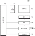
图1是示出基于所公开的技术的一些实现方式的示例图像传感器的框图。FIG. 1 is a block diagram illustrating an example image sensor based on some implementations of the disclosed technology.
图2是图1所示的像素阵列中所包括的像素的示例俯视图。FIG. 2 is an exemplary top view of pixels included in the pixel array shown in FIG. 1 .
图3是图2所示的像素的横截面图的示例。FIG. 3 is an example of a cross-sectional view of the pixel shown in FIG. 2 .
图4A至图4C是各自示出图3所示的第一外检测区域的示例的表示的图。4A to 4C are diagrams each showing a representation of an example of the first outer detection region shown in FIG. 3 .
图5是用于说明图3所示的第一外检测区域和第二外检测区域的功能的图的示例。FIG. 5 is an example of a diagram for explaining functions of the first outer detection area and the second outer detection area shown in FIG. 3 .
图6A和图6B是用于说明形成图3所示的第一检测区域和第二检测区域的工艺的像素的示图的示例。6A and 6B are examples of diagrams of pixels for explaining a process of forming the first detection area and the second detection area shown in FIG. 3 .
图7A和图7B是用于说明形成图3所示的第一检测区域和第二检测区域的工艺的示图的示例。7A and 7B are examples of diagrams for explaining a process of forming the first detection region and the second detection region shown in FIG. 3 .
图8A和图8B示出仿真结果,其示出包括具有对称结构和不对称结构的检测区域的相邻像素中的空穴电流的流动。8A and 8B illustrate simulation results showing the flow of hole currents in adjacent pixels including detection regions having symmetric structures and asymmetric structures.
图9A和图9B示出包括具有对称结构和不对称结构的检测区域的相邻像素中的解调对比度的仿真结果。FIGS. 9A and 9B show simulation results of demodulation contrast in adjacent pixels including detection regions having a symmetrical structure and an asymmetrical structure.
图中的各个元件的符号The symbols of the various components in the figure
100:图像传感器100: image sensor
110:像素阵列110: pixel array
120:行解码器120: row decoder
130:CDS130: CDS
140:ADC140: ADC
150:输出缓冲器150: output buffer
160:列解码器160: column decoder
170:定时控制器170: Timing controller
具体实施方式detailed description
本专利文献提供了图像感测装置的实现方式和示例。所公开的技术的一些实现方式提供了可减少和防止噪声和串扰的图像感测装置的设计。在一些实现方式中,当图像感测装置是间接型ToF感测装置时,在CAPD像素电路的操作期间可导致噪声和串扰。This patent document provides implementations and examples of image sensing devices. Some implementations of the disclosed technology provide designs of image sensing devices that reduce and prevent noise and crosstalk. In some implementations, when the image sensing device is an indirect ToF sensing device, noise and crosstalk may result during operation of the CAPD pixel circuit.
已对使用图像传感器测量范围和深度进行了许多开发和研究。在包括安全、医疗装置、汽车、游戏机、VR/AR和/或移动装置的各种领域中,对测量范围和深度的技术的需求快速增加。代表性技术包括三角测量系统、飞行时间系统或干涉测量系统。在这些系统当中,飞行时间系统由于其广泛的利用、高处理速度和成本优点而受到更多关注。飞行时间(ToF)系统使用所发射的光和所反射的光来测量距离。ToF系统可根据确定距离的是往返时间还是相位差而被分类为两种不同的类型,即,直接型和间接型。在直接型ToF系统中,通过计算往返时间来测量距离。在间接型ToF系统中,使用相位差来测量距离。直接型ToF系统通常用于汽车,因为其适合于测量长距离。间接型ToF系统通常用于与更短距离关联并且需要更快处理速度的游戏装置或移动相机。与直接型ToF系统相比,间接型ToF系统具有多个优点,包括具有更简单的电路、低存储器要求和相对低的成本。Much development and research has been done on measuring range and depth using image sensors. In various fields including security, medical devices, automobiles, game consoles, VR/AR and/or mobile devices, the demand for technology to measure range and depth is rapidly increasing. Representative techniques include triangulation systems, time-of-flight systems, or interferometry systems. Among these systems, time-of-flight systems have received more attention due to their widespread utilization, high processing speed, and cost advantages. Time-of-flight (ToF) systems use emitted and reflected light to measure distance. ToF systems can be classified into two different types, ie, a direct type and an indirect type, according to whether a round-trip time or a phase difference is used to determine a distance. In direct ToF systems, distance is measured by calculating the round-trip time. In an indirect ToF system, a phase difference is used to measure distance. Direct ToF systems are often used in automobiles because they are suitable for measuring long distances. Indirect ToF systems are typically used for gaming devices or mobile cameras that are associated with shorter distances and require faster processing speeds. Indirect ToF systems have several advantages over direct ToF systems, including having simpler circuitry, low memory requirements, and relatively low cost.
电流辅助光子解调器(CAPD)是一种用在间接ToF传感器中的像素电路。在CAPD中,使用通过施加基板电压而创建的多数载流子电流在像素电路中生成电子,并且使用电场的电位差来检测所生成的电子;由于使用多数载流子电流,所以可快速地检测电子。另外,通过检测设置在深位置中的电子,CAPD具有优异的效率。A current-assisted photonic demodulator (CAPD) is a pixel circuit used in indirect ToF sensors. In CAPD, electrons are generated in the pixel circuit using a majority carrier current created by applying a substrate voltage, and the generated electrons are detected using a potential difference of an electric field; since the majority carrier current is used, it can be detected quickly electronic. In addition, CAPD has excellent efficiency by detecting electrons disposed in deep positions.
以下,将参照附图描述所公开的技术的各种实施方式。然而,该描述并非旨在将本公开限于特定实施方式,应该解释为包括根据所公开的技术的实施方式的各种修改、等同形式和/或另选形式。Hereinafter, various embodiments of the disclosed technology will be described with reference to the accompanying drawings. However, this description is not intended to limit the present disclosure to specific embodiments, and should be construed to include various modifications, equivalents, and/or alternatives to embodiments according to the disclosed technology.
图1是示出根据所公开的技术的实施方式的图像传感器的示例的表示的框图。FIG. 1 is a block diagram illustrating a representation of an example of an image sensor in accordance with an implementation of the disclosed technology.
参照图1,图像传感器100可包括像素阵列110、行解码器120、相关双采样器(CDS)130、模数转换器(ADC)140、输出缓冲器150、列解码器160和定时控制器170。如图1所示的图像传感器100的各个组件仅是示例。可省略一些组件,或者可基于附加需要添加附加组件。Referring to FIG. 1 , an
图像传感器100可以是能够使用飞行时间(ToF)技术检测距对象的距离的范围/深度传感器。在一些实现方式中,照明装置(未示出)可朝着要由图像传感器100捕获的场景发射调制为预定波长的调制光,并且图像传感器100可感测从场景中的对象反射的调制光(入射光)并计算各个像素的深度信息。调制光和入射光可以是红外波长带内的光。根据图像传感器100与对象之间的距离,在调制光的发送与反射光的接收之间存在时间延迟,并且这种时间延迟被表示为图像传感器100所生成的信号之间的相位差。图像处理器(未示出)可通过计算从图像传感器100输出的信号之间的相位差来生成包括关于各个像素的深度信息的深度图像。The
在一些实现方式中,照明装置(未示出)和图像处理器(未示出)可与图像传感器100集成以形成单个单元。然而,所公开的技术不限于此,其它实现方式也是可能的。因此,照明装置和图像处理器可被配置为单独的单元而不与图像传感器100集成。In some implementations, an illumination device (not shown) and an image processor (not shown) can be integrated with
像素阵列110可包括以包括多行和多列的二维矩阵的形式布置的多个像素。各个像素可将入射光学信号转换为电信号。像素阵列110可从行解码器120接收驱动信号,并且可由驱动信号驱动。多个像素可包括被配置为生成深度图像的深度像素。根据实施方式,多个像素还可包括被配置为生成彩色图像的彩色像素。在这种情况下,可基于图像传感器100所生成的信号来生成3D图像。The
在一些实现方式中,各个深度像素可以是电流辅助光子解调器(CAPD)像素。深度像素的结构、操作和制造方法将稍后参照图2至图7B中所描绘的示例描述。In some implementations, each depth pixel may be a current assisted photonic demodulator (CAPD) pixel. The structure, operation, and manufacturing method of the depth pixel will be described later with reference to the examples depicted in FIGS. 2 to 7B .
像素阵列110被配置为包括CAPD像素,其中各个CAPD像素设置在两条列线之间,并且还可为各条列线设置用于处理从各条列线输出的像素信号的CDS(相关双采样器)130、ADC(模数转换器)140和输出缓冲器150。The
行解码器120可在定时控制器170的控制下驱动像素阵列110。行解码器120可生成行选择信号以在多行当中选择至少一行。行解码器120可相对于与至少一个所选行对应的像素依次启用像素重置信号和传输信号。作为模拟信号的参考信号和图像信号从所选行的各个像素生成并依次传输到相关双采样器130。这里,参考信号和图像信号可被统称为像素信号。The
相关双采样器130可依次采样并保持从像素阵列110提供给多条列线中的每一条的参考信号和图像信号。相关双采样器130可采样并保持与像素阵列110的各列对应的参考信号和图像信号的电平。The correlated
在定时控制器170的控制下,相关双采样器130可将从各列提供的参考信号和图像信号作为相关双采样信号传输到ADC 140。Under the control of the
ADC 140可将从相关双采样器130输出的各列的相关双采样信号转换为数字信号,并且可输出数字信号。ADC 140可基于各列的相关双采样信号以及从定时控制器170提供的斜坡信号来执行计数操作和计算操作,因此可生成去除了与各列对应的噪声(例如,各个像素特定的重置噪声)的数字型图像数据。The
ADC 140可包括像素阵列110的分别与列对应的多个列计数器,并且可使用列计数器将分别与列对应的相关双采样信号转换为数字信号。根据另一实施方式,ADC140可包括一个全局计数器,并且可使用从全局计数器提供的全局代码将与各列对应的相关双采样信号转换为数字信号。The
相关双采样器130和ADC 140可被统称为像素信号处理器。Correlated
输出缓冲器150可捕获并输出从ADC 140提供的各个列单元的图像数据。在定时控制器170的控制下,输出缓冲器150可暂时存储从ADC 140输出的图像数据。输出缓冲器150可作为对图像传感器100和与之连接的另一装置之间的传输(或处理)速度差异进行补偿的接口来操作。The
列解码器160可在定时控制器170的控制下选择输出缓冲器150的列,并且暂时存储在输出缓冲器150的所选列中的图像数据可依次输出。详细地,列解码器160可从定时控制器170接收地址信号,可通过基于地址信号生成列选择信号来选择输出缓冲器150的列,由此,可控制图像数据作为输出信号SO从输出缓冲器150的所选列输出。The
定时控制器170可控制行解码器120、ADC 140、输出缓冲器150和列解码器160。The
定时控制器170可向行解码器120、列解码器160、ADC 140和输出缓冲器150提供图像传感器100的各个组件的操作所需的时钟信号、用于定时控制的控制信号以及用于选择行或列的地址信号。根据实施方式,定时控制器170可包括逻辑控制电路、锁相环(PLL)电路、定时控制电路和通信接口电路。The
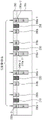
图2是图1所示的像素阵列中所包括的像素的俯视图的示例。图3是图2所示的像素的横截面图的示例。FIG. 2 is an example of a top view of pixels included in the pixel array shown in FIG. 1 . FIG. 3 is an example of a cross-sectional view of the pixel shown in FIG. 2 .
图2示出包括彼此相邻的第一像素P1和第二像素P2的俯视图200。像素阵列110可包括按照列和行布置的像素,并且至少一些像素可具有与第一像素P1或第二像素P2基本上相同或相似的结构。FIG. 2 shows a
第一像素P1可包括第一控制区域210和第二控制区域220以及第一检测区域230和第二检测区域240。第一控制区域210和第一检测区域230通常可称为第一解调节点(或第一插头区域),第二控制区域220和第二检测区域240通常可称为第二解调节点(或第二插头区域)。The first pixel P1 may include a
第一检测区域230可设置成围绕第一控制区域210的形状,并且第二检测区域240可设置成围绕第二控制区域220的形状。在图2中,第一检测区域230和第二检测区域240被示出为具有八边形形状,但所公开的技术不限于此,第一检测区域230和第二检测区域240可按照诸如圆形、多边形、闭环等的各种形状实现。在一些实现方式中,第一检测区域230和第二检测区域240可分别围绕第一控制区域210和第二控制区域220的部分。在一些实现方式中,第一检测区域230和第二检测区域240可分别不连续地围绕第一控制区域210和第二控制区域220。The
第二像素P2可包括第一控制区域250和第二控制区域260以及第一检测区域270和第二检测区域280。第一控制区域250和第一检测区域270可构成第一解调节点(或第一插头),第二控制区域260和第二检测区域280可构成第二解调节点(或第二插头)。The second pixel P2 may include a
第一检测区域270可被配置成围绕第一控制区域250的形状,并且第二检测区域280可被配置成围绕第二控制区域260的形状。在图2中,第一检测区域270和第二检测区域280被示出为具有八边形形状,但所公开的技术不限于此,第一检测区域270和第二检测区域280可按照诸如圆形、多边形、闭环等的各种形状实现。在一些实现方式中,第一检测区域270和第二检测区域280可分别围绕第一控制区域250和第二控制区域260的部分。在一些实现方式中,第一检测区域270和第二检测区域280可分别不连续地围绕第一控制区域250和第二控制区域260。The
包括在第一像素P1和第二像素P2中的组件210至280可通过介电层290物理地隔离。例如,介电层290可设置在第一控制区域210和第一检测区域230之间、第二控制区域220和第二检测区域240之间、第一控制区域250和第一检测区域270之间、以及第二控制区域260和第二检测区域280之间。介电层290可以是氧化物层,但所公开的技术不限于此。在一些实现方式中,第一像素P1和第二像素P2可包括诸如布线、浮置扩散区和晶体管的附加元件,但为了简明扼要,图2中省略那些元件。在一些实现方式中,布线可被配置为将驱动信号施加到第一像素P1和第二像素P2并配置像素信号的读取。The
参照图3,示出沿着图2的线A-A’截取的图像传感器的像素阵列中所包括的像素的横截面图300。Referring to FIG. 3 , there is shown a
第一像素P1和第二像素P2可设置在基板295处。基板295可以是P型半导体基板。将首先讨论第一像素P1的结构。第一控制区域210和第二控制区域220以及第一检测区域230和第二检测区域340可形成在基板295上。如图3所示,第一控制区域210和第二控制区域220可以是P型半导体区域,并且第一检测区域230和第二检测区域240可以是N型半导体区域。在第一像素P1中,第一外检测区域230a和第一内检测区域230b可设置在第一控制区域210的左侧和右侧。另外,第二内检测区域240b和第二外检测区域240a可设置在第二控制区域220的左侧和右侧。第一外检测区域230a和第一内检测区域230b对应于图2的第一检测区域230,第二内检测区域240b和第二外检测区域240a对应于图2的第二检测区域240。The first pixel P1 and the second pixel P2 may be disposed at the
在一些实现方式中,图像传感器100可以是前侧照明(FSI)型图像传感器,其中入射光入射到基板295的前表面(图3中的顶表面)上。在一些实现方式中,图像传感器100可以是后侧照明(BSI)型图像传感器,其中入射光入射到基板295的后表面(图3中的底表面)上。In some implementations,
第一控制区域210和第二控制区域220可分别从行解码器120接收第一解调控制信号V1和第二解调控制信号V2。第一解调控制信号V1与第二解调控制信号V2之间的电位差生成电场(或空穴电流),其控制由入射光在基板295中生成的信号载流子的流动。The
第一检测区域230和第二检测区域240可捕获信号载流子,并且可分别与具有特定电容的第一浮置扩散区和第二浮置扩散区联接。第一浮置扩散区和第二浮置扩散区中的每一个可联接到用于重置对应浮置扩散区的重置晶体管以及根据对应浮置扩散区的电位生成电信号的源极跟随器。源极跟随器可与选择晶体管联接,其用于向列线输出从源极跟随器输出的电信号。因此,与第一检测区域230和第二检测区域240中的每一个所捕获的信号载流子对应的信号可被输出到对应列线。可从行解码器120提供用于控制重置晶体管的重置控制信号以及用于控制选择晶体管的选择控制信号。The
以下,将更详细地描述第一像素P1的操作。Hereinafter, the operation of the first pixel P1 will be described in more detail.
在第一时段中,基板295可接收入射光并且响应于入射光的接收,在像素阵列中进行入射光的光电转换。作为光电转换的结果,入射光可在基板295中生成电子-空穴对;所生成的电子-空穴对的量可取决于入射光的强度。行解码器120可将第一解调控制信号V1施加到第一控制区域210,并且可将第二解调控制信号V2施加到第二控制区域220。第一解调控制信号V1的电压可高于第二解调控制信号V2的电压。例如,第一解调控制信号V1的电压可为1.2V,第二解调控制信号V2的电压可为0V。In the first period, the
由于第一解调控制信号V1的电压和第二解调控制信号V2的电压之间的电压差,可在第一控制区域210和第二控制区域220之间生成电场,并且电流可从第一控制区域210流到第二控制区域220。在这种情况下,基板295中生成的空穴朝着第二控制区域220移动,并且基板295中生成的电子朝着第一控制区域210移动。Due to the voltage difference between the voltage of the first demodulation control signal V1 and the voltage of the second demodulation control signal V2, an electric field may be generated between the
朝着第一控制区域210移动的电子可由与第一控制区域210相邻的第一检测区域230捕获。因此,基板295中生成的电子可用作信号载流子以用于检测入射光的量。Electrons moving toward the
由第一检测区域230捕获的电子可累积在第一浮置扩散区中并改变第一浮置扩散区的电位,并且源极跟随器和选择晶体管可将与第一浮置扩散区的电位对应的电信号输出到列线。电信号可以是图像信号或者可以包括图像信号。可对图像信号执行附加操作以从图像信号生成图像数据。这些附加操作可包括使用参考信号(在通过重置晶体管的重置之后与第一浮置扩散区的电位对应的电信号)的相关双采样和模数转换。The electrons captured by the
在第二时段中,第一解调控制信号V1和第二解调控制信号V2的电压电平的相对大小相对于第一时段改变。如针对第一时段讨论的,基板295可接收入射光并且响应于入射光的接收,像素阵列操作以执行入射光的光电转换。当入射光被光电转换时,入射光可根据入射光的强度在基板295中生成电子和空穴对。在第二时段期间,行解码器120可将第一解调控制信号V1施加到第一控制区域210,并且可将第二解调控制信号V2施加到第二控制区域220,第一解调控制信号V1具有低于第二解调控制信号V2的电压电平。例如,第一解调控制信号V1的电压可为0V,第二解调控制信号V2的电压可为1.2V。In the second period, the relative magnitudes of the voltage levels of the first demodulation control signal V1 and the second demodulation control signal V2 change with respect to the first period. As discussed with respect to the first period, the
由于第一解调控制信号V1的电压与第二解调控制信号V2的电压之间的电压差,可在第一控制区域210与第二控制区域220之间生成电场。在第二时段期间,电流可从第二控制区域220流到第一控制区域210。在这种情况下,基板295中生成的空穴朝着第一控制区域210移动,并且基板295中的电子朝着第二控制区域220移动。An electric field may be generated between the
朝着第二控制区域220移动的电子可由与第二控制区域220相邻的第二检测区域240捕获。因此,基板295中生成的电子可用作信号载流子以用于检测入射光的量。Electrons moving toward the
由第二检测区域240捕获的电子可累积在第二浮置扩散区中并改变第二浮置扩散区的电位,并且源极跟随器和选择晶体管可将与第二浮置扩散区的电位对应的电信号输出到列线。这种电信号可以是图像信号或者可以包括图像信号。基于图像信号,可生成图像数据。在一些实现方式中,可在执行使用参考信号(在通过重置晶体管的重置之后与第二浮置扩散区的电位对应的电信号)的相关双采样和模数转换之后获得图像数据。The electrons captured by the
图像处理器(未示出)可执行在第一时段中获得的图像数据和在第二时段中获得的图像数据的计算并获得相位差。在一些实现方式中,图像处理器可生成包括与各个像素的相位差对应的深度信息的深度图像。An image processor (not shown) may perform calculation of the image data obtained in the first period and the image data obtained in the second period and obtain a phase difference. In some implementations, the image processor may generate a depth image including depth information corresponding to a phase difference of each pixel.
由于第二像素P2的结构和操作与第一像素P1基本上相同,所以将省略对第二像素P2的详细描述。Since the structure and operation of the second pixel P2 are substantially the same as those of the first pixel P1, a detailed description of the second pixel P2 will be omitted.
第一像素P1和第二像素P2彼此相邻设置。当入射光被接收到基板295中时,可不仅在第一像素P1和第二像素P2中,而且在第一像素P1和第二像素P2周围的位置处(例如,第一像素P1和第二像素P2之间)生成电子。在第一像素P1和第二像素P2周围生成的那些电子如果被第一像素P1或第二像素P2捕获则可对图像提供不期望的影响。例如,在第一像素P1和第二像素P2周围生成的电子可在第一像素P1或第二像素P2中生成的深度信息中充当噪声,这使深度图像的质量劣化。The first pixel P1 and the second pixel P2 are disposed adjacent to each other. When incident light is received into the
为了消除或减小来自第一像素P1和第二像素P2周围生成的电子的这些不期望的影响,所公开的技术的一些实现方式提供检测区域,其根据检测区域的位置而具有彼此不同的厚度。例如,形成在对应控制检测区域的两侧的两个检测区域被设计为使得两个检测区域中更靠近像素边缘设置的一个检测区域可形成有相对更大的厚度,并且两个检测区域中更远离像素边缘设置的另一个检测区域可形成有相对更小的厚度。To eliminate or reduce these undesired effects from electrons generated around the first pixel P1 and the second pixel P2, some implementations of the disclosed technology provide detection regions that have different thicknesses from each other depending on the location of the detection regions . For example, the two detection areas formed on both sides of the corresponding control detection area are designed so that one of the two detection areas located closer to the edge of the pixel can be formed with a relatively larger thickness, and one of the two detection areas is more thick. Another detection area located away from the edge of the pixel may be formed with a relatively smaller thickness.
例如,与更远离第一像素P1的边缘设置的第一内检测区域230b和第二内检测区域240b中的每一个相比,更靠近第一像素P1的边缘设置的第一外检测区域230a和第二外检测区域240a中的每一个可形成有相对更大的厚度。For example, the first
第一外检测区域230a与第一内检测区域230b之间和第二外检测区域240a与第二内检测区域240b之间的深度差可考虑像素阵列的设计和特性(例如,像素的灵敏度、像素大小、相邻像素的隔离特征等)来确定。在一些实现方式中,第一外检测区域230a与第一内检测区域230b之间和第二外检测区域240a与第二内检测区域240b之间的深度差可实验地确定。The difference in depth between the first
图4A至图4C是各自示出图3所示的第一外检测区域的实施方式的表示的图。4A to 4C are diagrams each showing a representation of an embodiment of the first outer detection region shown in FIG. 3 .
参照图4A至图4C,更详细地示出图3所示的第一外检测区域230a的实施方式。Referring to FIGS. 4A to 4C , an embodiment of the first
第一外检测区域230a可包括具有不同掺杂浓度的区域。例如,第一外检测区域230a可包括N-区域230a-1和N+区域230a-2。N-区域230a-1掺杂有相对较低的N型杂质,N+区域230a-2掺杂有相对较高的N型杂质。在一些实现方式中,与第一外检测区域230a不同,第一内检测区域230b可仅包括N+区域而没有N-区域。The first
在一些实现方式中,N+区域230a-2捕获作为参照图3描述的信号载流子的电子,并且N-区域230a-1可不对电子的捕获做贡献。In some implementations,
图4A至图4C的实施方式示出N-区域230a-1形成得比N+区域230a-2更深。The embodiment of FIGS. 4A-4C shows that the N-
在图4A的实施方式中,N-区域230a-1的第一宽度W1可小于N+区域230a-2的第二宽度W2。在图4A中,第一宽度W1可表示与介电层290的顶表面接触的扩展N-区域(参见虚线)的宽度。第二宽度W2可意指与介电层290的顶表面接触的N+区域230a-2的宽度。在这种情况下,由于捕获电子的N+区域230a-2可与基板295接触,所以第一外检测区域230a的电子检测能力可改进。In the embodiment of FIG. 4A , the first width W1 of the N−
在图4B和图4C中,第一宽度W1和第二宽度可表示与介电层290的顶表面接触的N-区域230a-1和N+区域230a-2的宽度。In FIGS. 4B and 4C , the first width W1 and the second width may represent the widths of the N−
在图4B的实施方式中,N-区域230a-1的第一宽度W1可大于N+区域230a-2的第二宽度W2。在这种情况下,与图4C所示的情况相比,不捕获电子的N-区域230a-1以相对更大的厚度围绕N+区域230a-2。因此,第一外检测区域230a的电子阻挡能力可改进。这里,电子阻挡能力可意指防止或阻挡电子在像素内部与像素外部的区域(例如,对应像素与其相邻像素之间的区域)之间移动的能力。例如,两个相邻像素之间的区域中生成的电子不能容易地移动到任何像素的内部。在一些实现方式中,像素的内部可位于第一外检测区域23a的一侧,两个相邻像素之间的区域可位于第一外检测区域230的另一侧。In the embodiment of FIG. 4B, the first width W1 of the N−
在图4C的实施方式中,N-区域230a-1的第一宽度W1可与N+区域230a-2的第二宽度W2基本上相同。在这种情况下,由于不捕获电子的N-区域230a-1与图4B的实施方式相比以相对更小的厚度围绕N+区域230a-2,所以第一外检测区域230a的电子检测能力和电子阻挡能力可适当地平衡。In the embodiment of FIG. 4C , the first width W1 of the N−
尽管图4A至图4C示出第一外检测区域230a作为示例,但针对第一外检测区域230a讨论的描述可应用于其它外检测区域240a、270a和280a。Although FIGS. 4A-4C illustrate the first
图5是用于说明图3所示的第一外检测区域和第二外检测区域的功能的图的示例的表示。FIG. 5 is a representation of an example of a diagram for explaining functions of a first outer detection area and a second outer detection area shown in FIG. 3 .
参照图5,横截面图500示意性地示出在低电压施加到第一控制区域210和250并且高电压施加到第二控制区域220和260的情况下电子的流动。Referring to FIG. 5 , a
可在基板295的位于第一像素P1和第二像素P2内部的各个部分中生成电子。在第一像素P1和第二像素P2中,由于与从第二控制区域220和260流到第一控制区域210和250的电流对应的电场,所生成的电子可移动到第二控制区域220和260。移动到第二控制区域220和260的电子可被第二检测区域240和280捕获。Electrons may be generated in respective portions of the
也可在基板295的位于第一像素P1和与第一像素P1相邻布置的第二像素P2之间的部分中生成电子。然而,在第一像素P1和第二像素P2之间的位置处生成的电子可被第二外检测区域240a和第一外检测区域270a阻挡,这使得电子难以朝着对应控制区域移动。例如,电子无法移动到第二控制区域220或第一控制区域250,或者即使一些电子成功移动到第二控制区域220或第一控制区域250,与外检测区域240a和270a被设计为具有与内检测区域240b和270b相同的小厚度时的情况相比,那些电子的量可显著减少。在一些实现方式中,像素被设计为包括布置在对应控制区域的两侧以具有不对称结构的内检测区域和外检测区域,例如,外检测区域的厚度大于内检测区域的厚度。利用该结构,可有效地阻挡相邻像素之间的空穴电流的流动。因此,可通过防止相邻像素之间的电子移动(在图像传感器的操作中可能充当噪声)来改进图像传感器的性能。Electrons may also be generated in a portion of the
在图5的示例中,第一外检测区域270a和第二外检测区域240a阻挡在基板295的位于第一像素P1和与第一像素P1相邻的第二像素P2之间的部分中生成的电子的移动。因此,从第一像素P1或第二像素P2生成的深度信息中的噪声可显著减少,并且深度图像的质量可改进。In the example of FIG. 5, first
在一些实现方式中,低电压可被施加到第一控制区域210和第二控制区域260,高电压可被施加到第二控制区域220和第一控制区域250。当不同的电压被施加到布置在同一像素中的第一控制区域和第二控制区域并且相同的电压被施加到布置在相邻像素中的第一控制区域和第二控制区域时,可在各个像素内生成引起电子移动的电场,并且可抑制在基板295的位于第一像素P1和与第一像素P1相邻的第二像素P2之间的部分中生成的电子的移动。In some implementations, a low voltage may be applied to the
图6A、图6B、图7A和图7B是用于说明形成图3所示的第一检测区域和第二检测区域的工艺的图的示例。6A , 6B, 7A, and 7B are examples of diagrams for explaining a process of forming the first detection region and the second detection region shown in FIG. 3 .
在图6A和图6B中,使用阻挡层BK1至BK4来形成第一和第二外检测区域230a、240a、270a和280a的N-区域230a-1、240a-1、270a-1和280a-1。In FIGS. 6A and 6B, barrier layers BK1 to BK4 are used to form the N-
在一些实现方式中,通过氧化工艺在基板295上形成介电层290,并且通过注入P+型离子的离子注入工艺来形成第一和第二控制区域210、220、250和260。In some implementations, the
阻挡层BK1至BK4可设置在介电层290上以与对应检测区域230b、240b、270b和280b的各个部分交叠。例如,阻挡层BK1至BK4分别与第一检测区域230、第二检测区域240、第一检测区域270和第二检测区域280的一半交叠。第一和第二检测区域230、240、270和280的交叠的一半可对应于对应检测区域的内侧一半。阻挡层BK1至BK4可以是纳米线(NW)阻挡层或者可以包括纳米线(NW)阻挡层,但其它实现方式也是可能的。在一些实现方式中,与图6A和图6B的例示不同,阻挡层BK1至BK4中的每一个可具有彼此分裂的部分,并且分裂的部分可对应于第一和第二内检测区域230b、240b、270b和280b的图案。The barrier layers BK1 to BK4 may be disposed on the
在阻挡层BK1至BK4设置在介电层290上的情况下,可执行以相对高的能量注入N-型离子的离子注入工艺。结果,可在介电层290和基板295中形成掺杂N-杂质至与高能量对应的深度的N-区域230a-1、240a-1、270a-1和280a-1。In the case where the barrier layers BK1 to BK4 are disposed on the
在一些实现方式中,可执行注入N-型离子的离子注入工艺至少两次。例如,在设置阻挡层BK1至BK4之前,可设置具有比阻挡层BK1至BK4更宽的面积并从像素的内部延伸的附加阻挡层。在一些实现方式中,附加阻挡层可从像素的内部朝着像素的外部延伸。在一些实现方式中,附加阻挡层可设置在第一检测区域230上方以沿着水平方向与第一检测区域230的四分之三交叠。可在设置附加阻挡层的同时执行以高能量注入N-型离子的离子注入工艺。然后,在以高能量注入N-型离子之后,可设置阻挡层BK1至BK4。然后,可执行以低能量注入N-型离子的离子注入工艺。通过这些离子注入工艺,第一外检测区域和第二外检测区域可形成为具有比第一内检测区域和第二内检测区域更大的厚度。因此,可优化和改进第一外检测区域和第二外检测区域的电子阻挡能力和电子检测能力。In some implementations, the ion implantation process of implanting N-type ions may be performed at least twice. For example, before the barrier layers BK1 to BK4 are provided, an additional barrier layer having a wider area than the barrier layers BK1 to BK4 and extending from the inside of the pixel may be provided. In some implementations, the additional barrier layer can extend from the interior of the pixel towards the exterior of the pixel. In some implementations, an additional barrier layer may be disposed above the
在图7A和图7B中,为了形成第一和第二内检测区域230b、240b、270b和280b以及第一和第二外检测区域230a、240a、270a和280a的N+区域230a-2、240a-2、270a-2和280a-2,可去除阻挡层BK1至BK4,并且可执行以比注入N-型离子的离子注入工艺中所使用的能量更低的能量注入N+型离子的离子注入工艺。结果,可在介电层290和基板295中形成掺杂N+杂质至与低能量对应的深度的N+区域230a-2、240a-2、270a-2和280a-2以及第一和第二内检测区域230b、240b、270b和280b。In FIGS. 7A and 7B, in order to form the first and second
图8A和图8B示出仿真结果,其示出包括具有对称结构和不对称结构的检测区域的相邻像素中的空穴电流的流动。8A and 8B illustrate simulation results showing the flow of hole currents in adjacent pixels including detection regions having symmetric structures and asymmetric structures.
图8A示出包括具有对称结构的第一检测区域和第二检测区域的第一像素P1和第二像素P2中的空穴电流的流动。第一像素P1和第二像素P2彼此相邻。通过第一像素P1的第二控制区域220供应的0.68μA的空穴电流被分成朝着第一像素P1的第一控制区域210流动的0.39μA的空穴电流以及朝着第二像素P2的第一控制区域250流动的0.29μA的空穴电流。朝着第二像素P2的第一控制区域250流动的0.29μA的空穴电流变为在相邻像素P1和P2之间流动的电流。空穴电流的量(即,0.29μA)对应于通过第一像素P1的第二控制区域220供应的0.68μA的空穴电流的约43%,这导致相邻像素之间生成的电子移动并引起噪声。FIG. 8A illustrates the flow of hole currents in the first pixel P1 and the second pixel P2 including the first detection region and the second detection region having a symmetrical structure. The first pixel P1 and the second pixel P2 are adjacent to each other. The hole current of 0.68 μA supplied through the
图8B示出包括具有不对称结构的第一检测区域和第二检测区域的第一像素P1和第二像素P2中的空穴电流的流动。第一像素P1和第二像素P2彼此相邻。通过第一像素P1的第二控制区域220供应的0.53μA的空穴电流被分成朝着第一像素P1的第一控制区域210流动的0.38μA的空穴电流和朝着第二像素P2的第一控制区域250流动的0.15μA的空穴电流。因此,仅与0.53μA的整个空穴电流的约28%对应的0.15μA的空穴电流在相邻像素之间流动。与之相比,可以看出0.15μA的空穴电流与图8B的左侧相比显著低。FIG. 8B illustrates the flow of hole currents in the first pixel P1 and the second pixel P2 including the first detection region and the second detection region having an asymmetric structure. The first pixel P1 and the second pixel P2 are adjacent to each other. The hole current of 0.53 μA supplied through the
另外,尽管未示出,在附加仿真中确认,随着第一外检测区域和第二外检测区域的深度变深,在相邻像素之间流动的空穴电流的电流量减小。In addition, although not shown, it was confirmed in additional simulations that as the depths of the first outer detection region and the second outer detection region became deeper, the current amount of hole current flowing between adjacent pixels decreased.
图9A和图9B示出包括具有对称结构和不对称结构的检测区域的相邻像素中的解调对比度的仿真结果。FIGS. 9A and 9B show simulation results of demodulation contrast in adjacent pixels including detection regions having a symmetrical structure and an asymmetrical structure.
图9A示出包括具有对称结构的第一检测区域和第二检测区域并且彼此相邻的第一像素P1和第二像素P2中的解调对比度。作为指示CAPD像素的解调性能的指标,解调对比度表示在基板295中通过入射光生成的整个电子当中,在启用的解调节点(例如,包括施加更高电压的控制区域的解调节点)中捕获的电子的百分比。解调对比度指示像素的灵敏度。当各个像素具有均匀且高的解调对比度时,噪声性能优异。FIG. 9A shows demodulation contrast in a first pixel P1 and a second pixel P2 that include a first detection area and a second detection area having a symmetrical structure and are adjacent to each other. As an index indicative of the demodulation performance of a CAPD pixel, the demodulation contrast represents the demodulation point at an enabled demodulation point (e.g., a demodulation point including a control region where a higher voltage is applied) among the entire electrons generated in the
在第一检测区域和第二检测区域具有对称结构的情况下,第一像素P1和第二像素P2之间的解调对比度差异对应于通过从56%减去47%而获得的约9%。In the case where the first detection area and the second detection area have a symmetrical structure, the demodulated contrast difference between the first pixel P1 and the second pixel P2 corresponds to about 9% obtained by subtracting 47% from 56%.
图9B示出包括具有不对称结构的第一检测区域和第二检测区域并且彼此相邻的第一像素P1和第二像素P2中的解调对比度。在图9B中,第一像素P1和第二像素P2之间的解调对比度差异对应于通过从74%减去73%而获得的约1%。FIG. 9B shows the demodulation contrast in the first pixel P1 and the second pixel P2 that include the first detection area and the second detection area having an asymmetric structure and are adjacent to each other. In FIG. 9B , the demodulated contrast difference between the first pixel P1 and the second pixel P2 corresponds to about 1% obtained by subtracting 73% from 74%.
由于在基板295的位于第一像素P1和第二像素P2之间的部分中生成的电子可朝着第一像素P1或第二像素P2移动,所以那些电子可被第一像素P1或第二像素P2捕获,这使第一像素P1和第二像素P2的解调对比度性能和解调对比度均匀性劣化。然而,对于具有不对称结构的第一检测区域和第二检测区域的像素,由于第一检测区域和第二检测区域的不对称结构防止或减小在第一像素P1和第二像素P2之间生成的电子的移动,所以第一像素P1和第二像素P2的解调对比度性能和解调对比度均匀性可改进。Since electrons generated in a portion of the
应该理解,本文献的各种实施方式和本文所使用的术语并非旨在将本文献中所描述的技术特征限于特定实施方式,而是包括实施方式的各种修改、等同形式或另选形式。在附图的描述中,相似的标号可用于相似或相关的组件。It should be understood that the various embodiments of this document and the terms used herein are not intended to limit the technical features described in this document to specific embodiments, but include various modifications, equivalents or alternative forms of the embodiments. In the description of the figures, like reference numerals may be used for like or related components.
相关申请的交叉引用Cross References to Related Applications
本专利文献要求2019年7月1日提交于韩国知识产权局的韩国专利申请No.10-2019-0078699的优先权和权益,其整体通过引用并入本文。This patent document claims priority and benefit to Korean Patent Application No. 10-2019-0078699 filed with the Korean Intellectual Property Office on July 1, 2019, which is hereby incorporated by reference in its entirety.
Claims (20)
Applications Claiming Priority (2)
| Application Number | Priority Date | Filing Date | Title |
|---|---|---|---|
| KR1020190078699A KR102709669B1 (en) | 2019-07-01 | 2019-07-01 | Pixel, and Image Sensor including the same |
| KR10-2019-0078699 | 2019-07-01 |
Publications (2)
| Publication Number | Publication Date |
|---|---|
| CN112188128A CN112188128A (en) | 2021-01-05 |
| CN112188128B true CN112188128B (en) | 2022-12-23 |
Family
ID=73919876
Family Applications (1)
| Application Number | Title | Priority Date | Filing Date |
|---|---|---|---|
| CN201911017418.2A Active CN112188128B (en) | 2019-07-01 | 2019-10-24 | Pixels and image sensors including them |
Country Status (3)
| Country | Link |
|---|---|
| US (1) | US11011561B2 (en) |
| KR (1) | KR102709669B1 (en) |
| CN (1) | CN112188128B (en) |
Families Citing this family (3)
| Publication number | Priority date | Publication date | Assignee | Title |
|---|---|---|---|---|
| EP3742476B1 (en) * | 2019-05-20 | 2024-11-06 | Infineon Technologies AG | Method of implanting an implant species into a substrate at different depths |
| KR102883963B1 (en) * | 2021-01-12 | 2025-11-10 | 에스케이하이닉스 주식회사 | Image sensing device |
| KR20220141005A (en) * | 2021-04-12 | 2022-10-19 | 에스케이하이닉스 주식회사 | Image Sensing Device |
Citations (2)
| Publication number | Priority date | Publication date | Assignee | Title |
|---|---|---|---|---|
| CN106575658A (en) * | 2014-06-27 | 2017-04-19 | 软动力学传感器公司 | Majority current assisted radiation detector device |
| CN109644244A (en) * | 2017-08-09 | 2019-04-16 | 索尼半导体解决方案公司 | The control method of solid imaging element, electronic device and solid imaging element |
Family Cites Families (10)
| Publication number | Priority date | Publication date | Assignee | Title |
|---|---|---|---|---|
| KR101105635B1 (en) | 2007-09-05 | 2012-01-18 | 가부시키가이샤 시마쓰세사쿠쇼 | Solid-state imaging device and method for manufacturing the same |
| GB2474631A (en) * | 2009-10-14 | 2011-04-27 | Optrima Nv | Photonic Mixer |
| JP5680979B2 (en) | 2011-01-20 | 2015-03-04 | 浜松ホトニクス株式会社 | Solid-state imaging device |
| KR101869371B1 (en) * | 2011-07-21 | 2018-06-21 | 삼성전자주식회사 | Method of measuring a distance and three-dimensional image sensor performing the same |
| JP6489840B2 (en) * | 2015-01-20 | 2019-03-27 | エイブリック株式会社 | Hall element |
| US10690753B2 (en) * | 2016-03-04 | 2020-06-23 | Sony Corporation | Imaging apparatus and distance measurement system |
| KR102632100B1 (en) * | 2016-09-09 | 2024-02-01 | 주식회사 디비하이텍 | Photo-detector |
| JP7058479B2 (en) * | 2016-10-18 | 2022-04-22 | ソニーセミコンダクタソリューションズ株式会社 | Photodetector |
| JP6691101B2 (en) * | 2017-01-19 | 2020-04-28 | ソニーセミコンダクタソリューションズ株式会社 | Light receiving element |
| JP7175655B2 (en) * | 2018-07-18 | 2022-11-21 | ソニーセミコンダクタソリューションズ株式会社 | Light receiving element and ranging module |
-
2019
- 2019-07-01 KR KR1020190078699A patent/KR102709669B1/en active Active
- 2019-10-10 US US16/598,917 patent/US11011561B2/en active Active
- 2019-10-24 CN CN201911017418.2A patent/CN112188128B/en active Active
Patent Citations (2)
| Publication number | Priority date | Publication date | Assignee | Title |
|---|---|---|---|---|
| CN106575658A (en) * | 2014-06-27 | 2017-04-19 | 软动力学传感器公司 | Majority current assisted radiation detector device |
| CN109644244A (en) * | 2017-08-09 | 2019-04-16 | 索尼半导体解决方案公司 | The control method of solid imaging element, electronic device and solid imaging element |
Also Published As
| Publication number | Publication date |
|---|---|
| KR20210002880A (en) | 2021-01-11 |
| CN112188128A (en) | 2021-01-05 |
| KR102709669B1 (en) | 2024-09-26 |
| US11011561B2 (en) | 2021-05-18 |
| US20210005653A1 (en) | 2021-01-07 |
Similar Documents
| Publication | Publication Date | Title |
|---|---|---|
| JP6485880B2 (en) | Radiation detector device assisted by multiple currents | |
| US10896925B2 (en) | Detector device with majority current and isolation means | |
| US11221401B2 (en) | Detector device with majority current and a circuitry for controlling the current | |
| CN113938584B (en) | Image sensing device | |
| CN113727043B (en) | Image sensing device | |
| CN112188128B (en) | Pixels and image sensors including them | |
| CN101677106B (en) | Pixel cell, image sensor including a pixel cell, system having the same, and method of forming a pixel cell | |
| TWI910238B (en) | Image sensing device | |
| CN115996324A (en) | image sensing device | |
| US11218657B2 (en) | Pixel and image sensor including the same | |
| CN114765193B (en) | Image sensing device | |
| CN114554119B (en) | Image sensing device | |
| US12113085B2 (en) | Image sensing device | |
| CN114697580B (en) | Image sensing device | |
| US20250081651A1 (en) | Image sensing device including sloped isolation structure | |
| CN113766151A (en) | image sensing device | |
| CN114979517B (en) | Image sensing device | |
| US20240234466A1 (en) | Image sensing device and method for manufacturing the same | |
| US20230335571A1 (en) | Image sensing device | |
| US20230246058A1 (en) | Image sensing device |
Legal Events
| Date | Code | Title | Description |
|---|---|---|---|
| PB01 | Publication | ||
| PB01 | Publication | ||
| SE01 | Entry into force of request for substantive examination | ||
| SE01 | Entry into force of request for substantive examination | ||
| GR01 | Patent grant | ||
| GR01 | Patent grant |