Disclosure of Invention
Embodiments of the present application provide a control circuit for controlling a voltage conversion circuit to solve the problem of unstable voltage of a flying capacitor to some extent.
The field effect transistor in the embodiments of the present application may be a MOSFET, JFET, or other type of bidirectional field effect transistor. The electrical connection in the embodiment of the present application may be a physical contact connection, or may be an electrical connection implemented by a resistor, an inductor, a capacitor, or other electronic components.
For a better description of the embodiments of the present application, the following terms or abbreviations will be used:
PWM: pulse Width Modulation modulates the bias of a transistor base or a MOS tube grid according to the change of corresponding load to change the conduction time of the transistor or the MOS tube, thereby changing the output of the switching regulated power supply.
BUCK DCDC: step-down dc-dc conversion, the voltage at its output (load) is lower than the voltage at its input (supply) but the output current is greater than the input current.
In a first aspect, a control circuit for controlling a voltage conversion circuit is provided in an embodiment of the present application, the control circuit including a sawtooth wave generation circuit, a first voltage comparator, and a second voltage comparator. The sawtooth wave generating circuit is used for receiving and generating a first sawtooth wave signal and a second sawtooth wave signal according to a first reference voltage, a second reference voltage, a flying voltage and an input voltage, wherein when the first sawtooth wave signal is increased to the second reference voltage by a first slope, the second sawtooth wave signal is decreased to the first reference voltage, when the second sawtooth wave signal is increased to the second reference voltage by a second slope, the first sawtooth wave signal is decreased to the first reference voltage, the difference value of the first slope and the second slope is determined by the voltage difference value of the flying voltage and 1/2 times of the input voltage, the flying voltage is the voltage at two ends of a flying capacitor of the voltage converting circuit, and the input voltage is the input voltage of the voltage converting circuit; the first voltage comparator is used for receiving and comparing the regulating voltage and the first sawtooth wave signal and generating a first pwm signal according to the comparison result; the second voltage comparator is used for receiving and comparing the regulating voltage and the second sawtooth wave signal and generating a second pwm signal according to the comparison result; the regulated voltage is used for representing the degree of deviation of the voltage conversion circuit from a steady state in a normal working state. Wherein the two pwm signals are used to control the voltage conversion circuit.
Because of the characteristics of the first sawtooth wave signal and the second sawtooth wave signal, the duty ratios of the two pwm signals obtained by the voltage comparator are always equal and unchanged, so that the control circuit converts the difference value between the flying voltage and 1/2 times of input voltage into the slope difference of the two sawtooth wave signals, adjusts the frequency of the two pwm signals through the slope difference to adjust the time of the pwm signal at a high level, thereby adjusting the charging and discharging time of the flying capacitor, and enabling the flying capacitor to net flow out electric charge or net flow in electric charge in a complete period, so as to realize the voltage control of two ends of the flying capacitor, enable the voltage conversion circuit to be in a stable state, reduce the current ripple in the peripheral inductor, and improve the system efficiency.
In a possible design, the first voltage comparator compares the first sawtooth wave signal with the regulation voltage, and when the first sawtooth wave signal is smaller than the regulation voltage, the first pwm signal output by the first voltage comparator is at a high level, otherwise, the first pwm signal is at a low level; the second voltage comparator compares the second sawtooth wave signal with the regulating voltage, and when the second sawtooth wave signal is smaller than the regulating voltage, the second pwm signal output by the second voltage comparator is at high level, otherwise, the second pwm signal is at low level. Through the voltage comparator, the control circuit converts the sawtooth wave signal into a pwm signal to control the time of the pwm signal at a high level, thereby controlling the charging and discharging time of the flying capacitor.
In a possible design, the control circuit further includes an error amplifier configured to amplify a difference between a third reference voltage and a feedback voltage, and output the difference to the first voltage comparator and the second voltage comparator as the adjustment voltage, where the feedback voltage is used to represent an output voltage or an output current of the voltage conversion circuit, the output voltage is the output voltage of the voltage conversion circuit, the output current is the output current of the voltage conversion circuit, and the third reference voltage is used to represent an output voltage in a steady state when the conversion circuit normally operates. The error amplifier collects the actual output voltage of the voltage conversion circuit, and corrects the regulated voltage by the difference between the actual output voltage and the steady-state output voltage to stabilize the deviated actual output voltage.
In one possible design, the feedback voltage is equal to the output voltage of the voltage conversion circuit. The error amplifier collects the actual output voltage of the voltage conversion circuit, and corrects the regulated voltage by the difference between the actual output voltage and the steady-state output voltage to stabilize the deviated actual output voltage.
In a possible design, when the first sawtooth wave signal is smaller than the regulation voltage, the first voltage comparator outputs a high level, otherwise, the first voltage comparator outputs a low level; when the second sawtooth wave signal is smaller than the regulating voltage, the second voltage comparator outputs a high level, otherwise, the second voltage comparator outputs a low level. The first sawtooth wave signal and the second sawtooth wave signal are respectively passed through two comparators, so that the duty ratio of the pwm signal is controlled and kept unchanged while the pwm signal is obtained, and the duty ratio is used as a basis for adjusting the time that pwm is at a high level.
In one possible design, the sawtooth wave generating circuit includes a reference current generating circuit, a first oscillating circuit and a second oscillating circuit, wherein the reference current generating circuit is configured to receive the fly voltage and the input voltage, convert the fly voltage and 1/2 times the input voltage into a first reference current and a second reference current, and a current difference between the first reference current and the second reference current has a value proportional to a voltage difference between the fly voltage and 1/2 times the input voltage; the second reference voltage controls the first oscillating circuit to convert the first reference current into the first sawtooth wave signal, and a first slope of a rise of the first sawtooth wave signal is in direct proportion to the first reference current; the second reference voltage controls the second oscillating circuit to convert the second reference current into the second sawtooth wave signal, a second slope of a rise of the second sawtooth wave signal is proportional to the second reference current, and a difference between the first slope and the second slope is proportional to a current difference between the first reference current and the second reference current. The flying voltage is a voltage across a flying capacitor of the voltage conversion circuit, and the input voltage is an input voltage of the voltage conversion circuit. When the fly voltage is not stable, the difference value of the fly voltage and 1/2 times of input voltage is converted into the difference value of current by the sawtooth wave generating circuit, so that a sawtooth wave signal which is proportional to the current is generated to control the voltage converting circuit to adjust the fly voltage.
In one possible design, the reference current generating circuit is electrically connected to the first and second oscillating circuits at first and second nodes, respectively, and includes a voltage dividing circuit, a converting circuit, a first current source, and a second current source. The voltage division circuit is used for converting the input voltage into 1/2 times of input voltage; a conversion circuit for converting a difference between the flying voltage and 1/2 times the input voltage into a first intermediate current and a second intermediate current having the same current magnitude, the first intermediate current flowing from the conversion circuit to a first node, the second intermediate current flowing from a second node to the conversion circuit; a first current source for providing a first current source current flowing from a first node to ground; a second current source for providing a second current source current flowing from a second node to ground, the first current source current and the second current source current having the same magnitude; the first reference current flows from the first oscillation circuit to the first node, and the second reference current flows from the second oscillation circuit to the second node. The reference current generating circuit converts the difference value of the flying voltage and 1/2 times of input voltage into the difference value of current, and feeds the unsteady state of the voltage conversion circuit back to the control circuit, so that the control circuit is favorable for controlling the voltage conversion circuit in a steady state.
In one possible design, the reference current generating circuit is electrically connected to the first and second oscillating circuits at first and second nodes, respectively, and includes a voltage dividing circuit, a converting circuit, a first current source, and a second current source. The voltage division circuit is used for converting the input voltage into k/2 times of input voltage, wherein k is a positive number; a conversion circuit for converting a difference between k times the flying voltage and k/2 times the input voltage into a first intermediate current and a second intermediate current having the same current magnitude, the first intermediate current flowing from the conversion circuit to a first node, the second intermediate current flowing from a second node to the conversion circuit; a first current source for providing a first current source current flowing from a first node to ground; a second current source for providing a second current source current flowing from a second node to ground, the first current source current and the second current source current having the same magnitude; the first reference current flows from the first oscillation circuit to the first node, and the second reference current flows from the second oscillation circuit to the second node. The reference current generating circuit converts the difference value of k times of flying voltage and k/2 times of input voltage into the difference value of current, and the unsteady state of the voltage conversion circuit is fed back to the control circuit, so that the voltage difference between the flying voltage and 1/2 times of input voltage can be calculated more flexibly.
In one possible design, when the fly voltage is less than 1/2 times the input voltage, the first intermediate current and the second intermediate current are positive; when the flying voltage is greater than 1/2 times the input voltage, the first intermediate current and the second intermediate current are negative; when the fly voltage is 1/2 times the input voltage, the first intermediate current and the second intermediate current are 0. When the circuit is in an unstable state, the first intermediate current and the second intermediate current are not 0, so that the slopes of the two sawtooth wave signals are different, and in the changing process, the slopes of the two sawtooth wave signals are gradually equal, so that the two output currents change towards 0, and the circuit tends to a stable state.
In one possible design, the first oscillating circuit includes a first current mirror and a first output circuit, wherein the first current mirror is configured to generate a first mirror current according to a first ratio according to the first reference current, and the second reference voltage controls the first output circuit to convert the first mirror current into the first sawtooth wave signal according to the first ratio; correspondingly, the second oscillating circuit includes a second current mirror and a second output circuit, wherein the second current mirror is configured to generate a second mirror current according to the second reference current in a second ratio, and the second reference voltage controls the second output circuit to convert the second mirror current into the second sawtooth wave signal according to the second ratio. The first oscillating circuit and the second oscillating circuit convert the current into sawtooth wave signals, and the time of the pwm signal at high level is adjusted through the slope of the sawtooth wave signals, so that the pwm signal is in an adjustable state.
In one possible design, the first ratio and the second ratio are equal. The first current mirror and the second current mirror amplify the reference current in equal proportion, the same proportion is kept, and the synchronous regulation of the slopes of the first sawtooth wave signal and the second sawtooth wave signal is facilitated.
In one possible design, a ratio of the first mirror current to the first reference current is 6: 1, and a ratio of the second mirror current to the second reference current is 6: 1. Keeping the ratio to be 6: 1 is beneficial to making the slope change of the first sawtooth wave signal and the second sawtooth wave signal more sensitive.
In one possible design, the voltage divider circuit includes a first resistor and a second resistor connected in series and having equal resistance values, where one end of the first resistor receives the input voltage, the other end of the first resistor is electrically connected to one end of the second resistor, the other end of the second resistor is electrically connected to ground, and an electrical connection point of the two resistors outputs 1/2 times the input voltage. 1/2 times of input voltage is obtained through the voltage division circuit, so that compared with the flying voltage, the voltage conversion circuit receives the feedback unsteadiness of the voltage conversion circuit, and the voltage conversion circuit is regulated to be steady.
In a possible design, the first output circuit includes a first switch circuit and a first sawtooth wave capacitor connected in parallel, where one end of the first sawtooth wave capacitor is electrically connected to the first current mirror to receive a first mirror current and output the first sawtooth wave signal, and the other end of the first sawtooth wave capacitor receives the first reference voltage, and the second reference voltage controls the opening and closing of the first switch circuit; the second output circuit comprises a second switch circuit and a second sawtooth wave capacitor which are connected in parallel, wherein one end of the second sawtooth wave capacitor is electrically connected with the second current mirror to receive a second mirror image current and output the second sawtooth wave signal, the other end of the second sawtooth wave capacitor receives the first reference voltage, the second reference voltage controls the second switch circuit to be opened and closed, and the capacitance values of the first sawtooth wave capacitor and the second sawtooth wave capacitor are equal. The sawtooth wave capacitor is used for causing the voltage to rise and fall in the charging and discharging process, so that sawtooth wave signals are generated, and the voltage conversion circuit is controlled better.
In one possible design, when the first sawtooth wave signal increases to the second reference voltage, the second switch circuit is closed, and when the first sawtooth wave signal decreases to the first reference voltage, the second switch circuit is opened; when the second sawtooth wave signal is increased to the second reference voltage, the first switch circuit is closed, and when the second sawtooth wave signal is washed and is decreased to the first reference voltage, the first switch circuit is opened. The first switch circuit and the second switch circuit are controlled to be opened and closed through the second reference voltage, so that the first sawtooth wave signal and the second sawtooth wave signal fall when rising to the second reference voltage, and the aim of controlling the duty ratio of the pwm signal is fulfilled.
In one possible design, a positive input terminal of the first voltage comparator receives the regulated voltage, and a negative input terminal of the first voltage comparator receives the first sawtooth wave signal; the positive input end of the second voltage comparator receives the regulated voltage, and the negative input end of the second voltage comparator receives the second sawtooth wave signal. The pwm signal is generated by the comparator to better control the voltage conversion circuit.
In a second aspect, in an embodiment of the present application, there is provided a voltage conversion apparatus including a voltage conversion circuit for converting an input voltage into an output voltage according to control of a first pulse width modulation signal and a second pulse width modulation signal, and a control circuit for controlling the voltage conversion circuit, wherein the control circuit is the control circuit as in the first aspect and possible designs thereof.
Because of the characteristics of the first sawtooth wave signal and the second sawtooth wave signal, the duty ratios of the two pwm signals obtained by the voltage comparator are always equal and unchanged, so that the control circuit converts the difference value between the flying voltage and 1/2 times of input voltage into the slope difference of the two sawtooth wave signals, adjusts the frequency of the two pwm signals through the slope difference to adjust the time of the pwm signal at a high level, thereby adjusting the charging and discharging time of the flying capacitor, and enabling the flying capacitor to net flow out electric charge or net flow in electric charge in a complete period, so as to realize the voltage control of two ends of the flying capacitor, enable the voltage conversion circuit to be in a stable state, reduce the current ripple in the peripheral inductor, and improve the system efficiency.
In a third aspect, in an embodiment of the present application, there is provided a battery charging system, which includes a voltage conversion circuit, a control circuit, and a voltage stabilizing circuit, wherein the voltage stabilizing circuit is configured to convert an ac voltage into an input voltage of the voltage conversion circuit and input the input voltage to the voltage conversion circuit, the voltage conversion circuit is configured to convert the input voltage into an output voltage according to control of a first pulse width modulation signal and a second pulse width modulation signal and output the output voltage to a battery device, and the control circuit is configured to control the voltage conversion circuit, wherein the control circuit is the control circuit according to the first aspect and possible designs thereof.
Because of the characteristics of the first sawtooth wave signal and the second sawtooth wave signal, the duty ratios of the two pwm signals obtained by the voltage comparator are always equal and unchanged, so that the control circuit converts the difference value between the flying voltage and 1/2 times of input voltage into the slope difference of the two sawtooth wave signals, adjusts the frequency of the two pwm signals through the slope difference to adjust the time of the pwm signal at a high level, thereby adjusting the charging and discharging time of the flying capacitor, and enabling the flying capacitor to net flow out electric charge or net flow in electric charge in a complete period, so as to realize the voltage control of two ends of the flying capacitor, enable the voltage conversion circuit to be in a stable state, reduce the current ripple in the peripheral inductor, and improve the system efficiency.
Detailed Description
The technical solutions in the embodiments of the present application will be clearly and completely described below with reference to the drawings in the embodiments of the present application, and it is obvious that the described embodiments are only a part of the embodiments of the present application, and not all of the embodiments. All other embodiments, which can be derived by a person skilled in the art from the embodiments given herein without making any creative effort, shall fall within the protection scope of the present application.
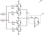
A voltage conversion circuit is a circuit that converts a dc input voltage into another dc output voltage, for example: a 3-step BUCK voltage conversion circuit (BUCK DCDC), or a 3-step boost voltage conversion circuit. A 3-step BUCK voltage conversion circuit (BUCK DCDC) is a voltage conversion circuit that converts a higher dc input voltage to a lower dc output voltage by receiving two pwm signals to control the opening and closing of switches in the voltage conversion circuit. The voltage conversion circuit includes a flying Capacitor (Fly Capacitor), and the input voltage charges and discharges the flying Capacitor during the period of opening and closing the switch to generate a stable output voltage. Fig. 1 shows a circuit diagram of a voltage conversion circuit 100, specifically, a 3-step down voltage conversion circuit shown in fig. 1. The voltage conversion circuit 100 receives a first pulse width modulation signal (pwm1 signal) and a second pulse width modulation signal (pwm2 signal) and uses the first pulse width modulation signal and the second pulse width modulation signal as control signals to convert an input voltage Vin having a higher voltage into an output voltage Vout having a lower voltage. The voltage conversion circuit 100 comprises 4 switches (Q1, Q2, Q3 and Q4), a control circuit (DRV1, DRV2, DRV3 and DRV4), and a flying capacitor CflyAnd peripheral circuit 110Wherein the peripheral circuit 110 includes a peripheral inductor LLAnd a peripheral capacitor CLAnd an equivalent load resistance RL. The switches Q1, Q2, Q3, and Q4 may be Field Effect Transistors (FETs), such as Metal-Oxide-Semiconductor Field-Effect transistors (MOSFETs), or Junction Field-Effect transistors (JFETs), or other types of transistors.
As shown in fig. 1, in the voltage conversion circuit 100, 4 switches Q1, Q2, Q3 and Q4 are connected in series in the forward direction, and the drain of the switch Q1 is electrically connected to the input voltage source Vin, and the source of the switch Q4 is electrically connected to the ground. Flying capacitor CflyIs electrically connected to the source of switch Q1 at one end and to the source of switch Q3 at the other end. Peripheral inductance L in peripheral circuit 110LOne end of the first and second switches is electrically connected with the source electrode of the switch Q2, and the other end is respectively connected with the peripheral capacitor CLAnd a load resistance RLIs electrically connected to a peripheral capacitor CLAnd a load resistance RLThe other end of the first and second electrodes is electrically connected to ground. The control circuit DRV1 receives the pwm1 signal and controls the gate of the switch Q1 to control the switch Q1 to be turned on and off; the control circuit DRV2 receives the pwm2 signal and controls the gate of the switch Q2 to control the switch Q2 to be turned on and off; the control circuit DRV3 receives the pwm2 signal, and controls the grid of the switch Q3 after the pwm2 signal is inverted so as to control the on-off of the switch Q1; the control circuit DRV4 receives the pwm1 signal, inverts the pwm1 signal, and controls the gate of the switch Q4 to turn on and off the switch Q4.
In the voltage conversion circuit 100, the pwm1 signal controls the opening and closing of the switches Q1 and Q4, and the pwm2 signal controls the opening and closing of the switches Q2 and Q3. When the circuit is in steady state, the high level of the pwm1 signal closes switch Q1 and opens switch Q4, and the low level of the pwm1 signal opens switch Q1 and closes switch Q4. Similarly, the high of the pwm2 signal closes switch Q2 and opens switch Q3, and the low of the pwm2 signal opens switch Q2 and closes switch Q3. When the voltage conversion circuit 100 is in a steady state, the pwm1 signal and the pwm2 signal have the same frequency, the same duty cycle, but are 180 ° out of phase.
Fig. 2(a) shows waveforms of the voltage conversion circuit 100 in a steady state. The operation of the voltage converting circuit 100 is illustrated with a complete period T1-T5. It is noted that the duty cycle in this application is the ratio of the time when the pwm signal is at a high level to the time difference between the rising edges of the two pwm signals. For example, the duty cycle of the pwm1 signal may be expressed as (T2-T1)/(T3-T1), while the duty cycle of the pwm2 signal may be expressed as (T4-T3)/(T5-T3). Accordingly, the frequency of a pwm signal in this application is the inverse of the time difference between the rising edge of the pwm signal and the rising edge of another pwm signal. For example, the frequency of the pwm1 signal may be expressed as 1/(T3-T1), while the frequency of the pwm2 signal may be expressed as 1/(T5-T3).
At the stages T1 to T2, the pwm1 signal is at a high level and the pwm2 signal is at a low level, so that the switch Q1 is closed, Q2 is open, Q3 is closed, and Q4 is open, and the voltage path formed at this time is as shown in fig. 3 (a). Wherein, the flying capacitor CLIn a charging state, a flying voltage V across itflyIncreasing with time, flying capacitor CLCurrent I inflyThe direction is from node a to node C. Peripheral inductance LLThe current IL in (b) becomes larger with time.
At the stage T2 to T3, the pwm1 signal is low and pwm2 signal is low, so that the switch Q1 is open, Q2 is open, Q3 is closed, and Q4 is closed, and the voltage path formed at this time is as shown in fig. 3 (b). Wherein, the flying capacitor CLOnly one end is electrically connected with the ground end through a switch and is in a floating state, and the flying voltage V at the two endsflyRemain unchanged. Peripheral inductance LLThe current IL in (1) becomes smaller with time.
At the stage T3 to T4, the pwm1 signal is low and pwm2 signal is high, so that the switches Q1 are open, Q2 is closed, Q3 is open and Q4 is closed, and the voltage path formed at this time is as shown in fig. 3 (c). Wherein, the flying capacitor CLIn a discharge state, a flying voltage V across itflyDecreasing with time, current IflyThe direction is from node C to node a. Peripheral inductance LLThe current IL in (b) becomes larger with time, and the increasing slope is the same as the increasing amplitude in the stages T1 to T2.
At the stage T4-T5, the pwm1 signal isLow, pwm2 signal is low, so switch Q1 is open, Q2 is open, Q3 is closed, and Q4 is closed, and the voltage path formed at this time is as shown in fig. 3 (d). Wherein, the flying capacitor CLOnly one end is electrically connected with an input voltage source Vin through a switch, the input voltage source Vin is in a floating state, and flying voltages V at two ends of the input voltage source VinflyRemain unchanged. Peripheral inductance LLThe current IL in (1) becomes smaller with time, and the slope of the fall is the same as the magnitude of the fall at the stages T2 to T3.
In the voltage conversion circuit 100, a flying capacitor CflyVoltage V acrossflyNeeds to be stabilized at Vin/2 to make the circuit operate in steady state. The application of flying capacitor voltage V is typically accomplished by varying the duty cycles of the pwm1 and pwm2 signalsflyAnd (4) adjusting. For example, the duty cycle of the pwm1 signal before conditioning is 20% and the duty cycle of the pwm2 signal is 20%, when V isflyThe voltage across is less than Vin/2. The duty cycle of the pwm1 signal is adjusted to 30% and the duty cycle of the pwm2 signal is adjusted to 10%, so that the time for the switches Q1 and Q3 to be simultaneously closed is increased, namely the flying capacitor C is increasedflyWhile making the time for which switches Q2 and Q4 are simultaneously closed shorter, i.e., reducing flying capacitor C, from charging time T2-T1flyDischarge time T4-T3. Due to flying capacitor CflyCurrent I inflyEqual to the current IL in the peripheral inductor LI, when the average value of the current IL in the charging process and the average value in the discharging process are kept equal, and after a complete period, the flying capacitor CflyIn which there is a static charge build-up which can lead to VflyAnd (4) rising. Conversely, if the duty cycle of pwm1 signal is adjusted down and the duty cycle of pwm2 signal is adjusted up, then V can be adjusted downflyAnd (5) turning down.
In actual operation, the peripheral inductance LLThe average value of the current IL during charging and the average value during discharging are generally not equal. As shown in fig. 2(b), which is a waveform diagram of the voltage converting circuit 100 continuously in the regulated state (in the non-steady state), in the period from T4 to T5, the peripheral inductance L is short in durationLThe current IL in the inductor is unable to drop to the current value at the time T3, i.e. the average value of the current IL is unable to remain unchanged, resulting in the peripheral inductance LLThe ripple of the current IL in (1) is too large, affecting the efficiency of the system. To stabilize the voltage conversion circuit 100, the voltage across the flying capacitor, V, must be maintainedflyIs stabilized at Vin/2.
The application provides a control circuit, which is used for generating two pwm signals according to an input voltage and an output voltage of a voltage conversion circuit and a plurality of reference voltages, wherein the input voltage and the output voltage are used as feedback voltage signals to adjust the time of the pwm signals at a high level, so as to adjust the charging and discharging time of a flying capacitor, and to realize the adjustment of the flying voltage in the voltage conversion circuit.
As shown in fig. 4, a control circuit 400, the control circuit 400 can be used to control the voltage converting circuit. The control circuit 400 includes a sawtooth wave generation circuit 410, an error amplifier 420, a first voltage comparator 430, and a second voltage comparator 440. Sawtooth wave generating circuit 410 receives flying capacitor CflyVoltage V acrossflyThe input voltage Vin of the voltage conversion circuit 100, and the first reference voltage Vref1 and the second reference voltage Vref2 according to Vin and VflyVref1 and Vref2 generate a first Vsaw1 and a second Vsaw2 sawtooth signal. When the voltage value of the first sawtooth wave signal Vsaw1 increases to the second reference voltage Vref2 with a slope1, the second sawtooth wave signal Vsaw2 decreases to the first reference voltage Vref1, and when the voltage value of the second sawtooth wave signal Vsaw2 increases to the second reference voltage with a slope2, the first sawtooth wave signal Vsaw1 decreases to the first reference voltage Vref1 with a slope Vref 2. The sawtooth wave generating circuit 410 generates a sawtooth wave according to the flying voltage VflyAnd 1/2 times the input voltage Vin to control and determine the difference between slope1 and slope 2.
The error amplifier 420 receives the third reference voltage Vref3 and the feedback voltage Vfb, amplifies a difference between the third reference signal and the feedback voltage Vfb, and outputs the amplified difference as an err signal (i.e., a regulated voltage) to the first voltage comparator 430 and the second voltage comparator 440. The third reference voltage Vref3 is determined according to the output voltage Vout of the voltage converting circuit 100 in steady state during normal operation, i.e., the third reference voltage Vref3 can represent the operation of the voltage converting circuit 100 in integer divisionThe output voltage at steady state. The feedback voltage Vfb is determined according to an output voltage Vout of the voltage conversion circuit or an output current Iout of the voltage conversion circuit 100, for example, the output current Iout may be a peripheral inductor LLAverage value of the current IL in (1). In one possible embodiment, the feedback voltage Vfb is equal to the output voltage Vout. Therefore, the err signal (i.e., the regulated voltage) is used to characterize the degree to which the voltage conversion circuit 100 deviates from the steady state during normal operation, for example, the larger the output voltage Vout of the voltage conversion circuit 100 actually deviates from the steady state during normal operation, the larger the voltage value of the err signal (the regulated voltage) is.
The first voltage comparator 430 receives the first sawtooth wave signal Vsaw1 generated by the sawtooth wave generating circuit 410 and the err signal output by the error amplifier 420, and outputs a pwm1 signal by comparing the magnitude relationship between the first sawtooth wave signal Vsaw1 and the err signal; the similar second voltage comparator 440 receives the second sawtooth wave signal Vsaw2 generated by the sawtooth wave generating circuit 410 and the err signal output by the error amplifier 420, and outputs a pwm2 signal by comparing the magnitude relationship between the second sawtooth wave signal Vsaw2 and the err signal. The pwm1 signal and the pwm2 signal are used to control the voltage conversion circuit 100. The err signal is a regulation voltage for regulating the duty ratio of the pwm1 signal and the pwm2 signal. Hereinafter, for convenience of description, the regulation voltage is represented by an err signal.
The first and second sawtooth wave signals Vsaw1 and Vsaw2 generate pwm1 and pwm2 signals after passing through the first and second voltage comparators 430 and 440, the duty ratios of the pwm1 and pwm2 signals remain unchanged regardless of whether they are in regulation or in steady state, and the duty ratios are equal to err/Vref 2. Therefore, when the control circuit 400 controls the voltage conversion circuit 100 using the pwm1 signal and the pwm2 signal, the fly voltage V is adjustedflyThe amount of the voltage deviated 1/2 times from the input voltage Vin is converted into the difference between the slope1 and the slope2, and the two sawtooth wave signals are output with the above slopes such that the pwm1 signal and the pwm2 signal generated by the first voltage comparator 430 and the second voltage comparator 440 are duty-cycledUnder the condition of constant ratio, the frequency of the pwm1 signal and the pwm2 signal can be adjusted to adjust the time when the pwm1 signal and the pwm2 signal are at high level, so as to adjust the flying capacitor CflyThe charging and discharging time of the flying capacitor C is ensured to be the net outflow charge or the net inflow charge in a complete charging and discharging period so as to realize the purpose of charging and discharging the flying capacitor CflyVoltage V acrossflyControlled at Vin/2 to make the voltage conversion circuit 100 in a stable state, thereby reducing the peripheral inductance LLThe ripple of the current IL in the system improves the system efficiency.
The first voltage comparator 430 and the second voltage comparator 440 may be a single-limit comparator, a hysteresis comparator, a window comparator, or other types of voltage comparators, and the present application does not limit the types or specific structures of the voltage comparators, nor limits the positive and negative connections of the input terminals of the voltage comparators. In one possible embodiment, the first voltage comparator 430 compares the magnitudes of the Vsaw1 signal and the err signal, and outputs pwm1 signal at a high level when the Vsaw1 signal is smaller than the err signal, and outputs pwm1 signal at a low level otherwise; the second voltage comparator 440 compares the magnitudes of the Vsaw2 signal and the err signal, and outputs a pwm2 signal at a high level when the Vsaw2 signal is less than the err signal, and outputs a pwm2 signal at a low level otherwise. In another possible implementation, when the Vsaw1 signal is less than the err signal, the pwm1 signal is output low, otherwise the pwm1 signal is output high; when the Vsaw2 signal is less than the err signal, the pwm2 signal is low, otherwise the pwm2 signal is high. In the present application, the err signal is electrically connected to the positive inputs of the first voltage comparator 430 and the second voltage comparator 440, respectively, and the negative terminal of the first voltage comparator 430 receives the first sawtooth signal Vsaw1, and the negative terminal of the second voltage comparator 440 receives the second sawtooth signal Vsaw 2. The error amplifier 420 may be a transistor amplifier circuit or a field effect transistor amplifier circuit, and the present application does not limit the type or specific structure of the amplifier, nor limits the positive and negative connections of the input terminal of the error amplifier 420.
Error amplifier 420 receives Vref3 and Vfb and amplifies the difference between Vref3 and Vfb for output as an err signal. The feedback voltage Vfb is determined by the output voltage Vout or the output current Iout of the voltage conversion circuit 100, and may be, for example, the actual output voltage Vout, 1/2 times the output voltage Vout, or a voltage value converted by the output current Iout. In one possible implementation, the error amplifier 420 may directly calculate and amplify the actual output voltage Vout of the voltage converting circuit 100 and the third reference voltage Vref3 as err signals, where the third reference voltage Vref3 is the output voltage in a steady state when the voltage converting circuit 100 is operating normally. For example, the output voltage of the voltage converting circuit 100 in the steady state during normal operation is 20V, and the actual output voltage thereof in the non-steady state is 19V, and at this time, the third reference voltage Vref3 received by the error amplifier 420 is 20V, and the error signal (i.e., the actual output voltage) is 19V, so that the error amplifier 420 amplifies the difference value with the magnitude of 1V and outputs the difference value as the err signal.
Fig. 5 is a schematic diagram of a sawtooth wave generation circuit 410. The sawtooth wave generating circuit 410 includes a reference current generating circuit 411, a first oscillating circuit 412, and a second oscillating circuit 413. Wherein the reference current generating circuit 411 is based on the flying capacitor CflyFlying voltage V acrossflyAnd an input voltage Vin for generating a first reference current Iref1 and a second reference current Iref2, the difference between the Iref1 and the Iref2 and the flying voltage VflyAnd 1/2 times the voltage difference of the input voltage Vin. The second reference voltage Vref2 controls the first oscillating circuit 412 to convert the first reference current Iref1 into the first sawtooth wave signal Vsaw1, and the second reference voltage Vref2 controls the second oscillating circuit 413 to convert the second reference current Iref2 into the second sawtooth wave signal Vsaw2, wherein the rising slope1 of the first sawtooth wave signal Vsaw1 is proportional to the current value of the first reference current Iref1, the rising slope2 of the second sawtooth wave signal Vsaw2 is proportional to the current value of the second reference current Iref2, and slope1-slope2 are proportional to the current values of Iref1-Iref 2.
The reference current generating circuit 411 may have a circuit structure as shown in fig. 5, and includes a converting circuit Gm, a voltage dividing circuit DIV, a first current source ib1, and a second current source ib 2. The voltage divider DIV is used to convert the input voltage Vin into 1/2 times the input voltage Vin. For example, the resistor R1 and the resistor R2 are connected in series, one end of the resistor R1 receives the input voltage Vin, the other end is electrically connected to the node a with one end of the resistor R2, and the other end of the resistor R2 is electrically connected to the ground. In one possible implementation, the resistors R1 and R2 are equal in value to obtain half of the input voltage Vin at node a, i.e., 1/2 Vin.
Two input ends of the conversion circuit Gm respectively receive the flying capacitor CflyVoltage V acrossflyAnd 1/2 times the input voltage 1/2Vin, i.e., the voltage of node A, and receives VflyThe voltage difference of the voltage and 1/2Vin is converted into a current io1 and a current io2, and the currents are output through a node B and a node C. The current io1 and the current io2 have the same magnitude and opposite directions, and the current values of the current io1 and the current io2 are the same as the above-mentioned VflyAnd 1/2 Vin. The positive and negative of the current io1 and the current io2 and VflyAbout 1/2Vin, particularly when V isfly< 1/2Vin, the current io1 and the current io2 are positive; when V isflyWhen the voltage is greater than 1/2Vin, the current io1 and the current io2 are negative; when V isflyCurrent io1 and current io2 are 0, 1/2 Vin. It should be noted that the voltage actually input to the conversion circuit Gm may be kVflyAnd k/2Vin, where k may be a positive integer or other positive number, and the application does not limit the specific voltage input to the conversion circuit Gm. The conversion circuit Gm is actually converting VflyThe voltage difference of 1/2Vin is converted into two currents in opposite directions. For example, the conversion circuit Gm may convert 1/2VflyThe voltage difference of 1/4Vin is converted into a current io1 and a current io 2.
In one possible implementation, the direction of current io1 flows from the conversion circuit Gm to the node B, and the direction of current io2 is opposite, flowing from the node C to the conversion circuit Gm. The first current source is electrically connected to node B and ground, providing a current ib from node B to ground, so the current Iref1 input into the first current mirror 4121 can be expressed as:
Iref1=ib-io1,
wherein the current direction of Iref1 is from first current mirror 4121 to node B; similarly, a second current source is electrically connected to node C and ground to provide a current ib of equal magnitude from ground to node C, and thus the current Iref2 input into the second current mirror 4131 may be expressed as
Iref2=ib+io2,
Where the current direction of Iref2 is from second current mirror 4131 to node C. Since Iref2-Iref1 is io2+ io1, and io1 and io2 are both equal in size and equal in size to VflyAnd 1/2Vin, so Iref2-Iref1 is proportional to VflyAnd 1/2 Vin.
As shown in fig. 5, the first oscillation circuit 412 includes a first current mirror 4121 and a first output circuit 4122. The first current mirror 4121 is configured to generate a first mirror current Imr1 according to a first reference current Iref1, the first output circuit 4122 receives the first mirror current Imr1, and the second reference voltage Vref2 controls the first output circuit 4122 to convert the first mirror current Imr1 into a first sawtooth wave signal Vsaw1, where a slope1 of the Vsaw1 is proportional to the Iref 1. Accordingly, the second oscillation circuit 413 includes a second current mirror 4131 and a second output circuit 4132. The second oscillation circuit 413 includes a second current mirror 4131 and a second output circuit 4132. The second current mirror 4131 is configured to generate a second mirror current Imr2 according to a second reference current Iref2, the second output circuit 4132 receives the second mirror current Imr2, and the second reference voltage Vref2 controls the second output circuit 4132 to convert the second mirror current Imr2 into a second sawtooth wave signal Vsaw2, where a slope2 of the Vsaw2 is proportional to the Iref 2.
The first current mirror 4121 and the second current mirror 4131 may have a circuit configuration as shown in fig. 5. The first current mirror 4121 will be described as an example. The first current mirror 4121 may include a first fet M1 and a second fet M2, wherein sources of the first fet M1 and the second fet M2 are electrically connected and electrically connected to the analog voltage source AVDD, gates of the first fet M1 and the second fet M2 are electrically connected, a drain of the first fet M1 is electrically connected to the first output circuit 4122, and a gate and a drain of the second fet M2 are electrically connected to the node B. The current value proportion of the first reference current Iref1 and the first mirror current Imr1 is realized by adjusting the proportion of the device sizes of the first field effect transistor M1 and the second field effect transistor M2, that is, the width-to-length ratio (W/L) of the channel. For example, by adjusting the ratio of the device dimensions described above, such that:
Imr1/Iref1=Imr2/Iref2,
namely, the first reference current Iref1 and the second reference current Iref2 obtain corresponding mirror currents through proportional mirroring. In one possible embodiment, the device size ratio of the first fet M1 and the second fet M2 is 6: 1, i.e., the first mirror current Imr1 is 6Iref 1. Similarly, the second current mirror 4131 has a similar structure to the first current mirror 4121, and the description thereof is omitted. In one possible embodiment, the ratio of the third fet M3 to the fourth fet M4 is 6: 1, i.e., the obtained second mirror current Imr2 is 6Iref 2. It should be noted that the present application does not limit the specific structure of the first current mirror 4121 and the second current mirror 4131, and they may be MOS Transistor current mirrors, BJT (Bipolar Junction Transistor) current mirrors, etc.
The first output circuit 4122 and the second output circuit 4132 may have a circuit configuration as shown in fig. 5. The first output circuit 4122 will be described as an example. The first output circuit 4122 includes a first sawtooth wave capacitor Csaw1 and a first switch circuit S1 connected in parallel, where one end of the first sawtooth wave capacitor Csaw1 receives the first mirror current Imr1 output by the first current mirror 4121 at a node D, and the other end receives a first reference voltage Vref1, and a voltage at the node D is a first sawtooth wave voltage Vsaw 1. Wherein the second reference voltage Vref2 is used to control the opening and closing of the first switch circuit S1. Similarly, the second output circuit 4132 has a similar structure to the first output circuit 4122, and includes a second sawtooth wave capacitor Csaw2 and a second switch circuit S2 connected in parallel, wherein one end of the second sawtooth wave capacitor Csaw2 receives the second mirror image current Imr2 output by the second current mirror 414 at a node E, and the other end receives a first reference voltage Vref1, and a voltage at the node E is a second sawtooth wave voltage Vsaw 2. Wherein the second reference voltage Vref2 is used to control the opening and closing of the second off circuit S2. When the first sawtooth wave signal Vsaw1 increases to Vref2, the first switch circuit S1 is closed, at which time the first sawtooth wave capacitor Csaw1 discharges, the first sawtooth wave signal Vsaw1 falls, and when the first sawtooth wave signal Vsaw1 falls to Vref1, the first switch circuit is opened; similarly, when the second sawtooth wave signal Vsaw2 increases to Vref2, the second switch circuit S2 is closed, the second sawtooth wave capacitor Csaw2 discharges, the second sawtooth wave signal Vsaw2 falls, and when the second sawtooth wave signal Vsaw2 falls to Vref1, the second switch circuit opens. The capacitance values of the first sawtooth capacitor Csaw1 and the second sawtooth capacitor Csaw2 are equal so that the two slope changes are symmetrical when slope1 and slope2 are adjusted.
The operation of the sawtooth wave generating circuit 410 is illustrated by the example of waveforms in fig. 6. The waveform diagram shown in fig. 6 is an input/output waveform when the sawtooth wave generating circuit 410 is in a steady state, and at this time, the slope1 of the rising slope of the first sawtooth wave signal Vsaw1 is equal to the slope2 of the rising slope of the second sawtooth wave signal Vsaw 2.
In the stages T1 to T3, the first sawtooth wave signal Vsaw1 and the second sawtooth wave signal Vsaw2 respectively rise at the slopes of slope1 and slope2, and slope1 is equal to slope 2. Since the Vsaw1 signal is higher than the err signal, the pwm1 signal generated through the first voltage comparator cmp1 is low. Since the Vsaw2 signal is lower than the err signal during the periods T1-T2, the pwm2 signal generated by the second voltage comparator cmp2 is high. At time T3, the second sawtooth wave signal Vsaw2 increases to the second reference voltage Vref2, and the first switch circuit S1 is closed, so that the first sawtooth wave signal Vsaw1 rapidly drops to the first reference voltage Vref 1.
In the stages T3 to T5, the first sawtooth wave signal Vsaw1 and the second sawtooth wave signal Vsaw2 respectively rise at the slopes of slope1 and slope2, and slope1 is equal to slope 2. Since the Vsaw2 signal is higher than the err signal, the pwm2 signal generated through the second voltage comparator cmp2 is low. Since the Vsaw1 signal is lower than the err signal during the periods T3-T4, the pwm1 signal generated by the first voltage comparator cmp1 is high. At time T5, the first sawtooth signal Vsaw1 increases to the second reference voltage Vref2, and the second switch circuit S1 is closed, such that the second sawtooth signal Vsaw2 rapidly decreases to the first reference voltage Vref 1.
As shown in fig. 6, when the sawtooth wave generating circuit 410 is in a steady state, the slopes of the first sawtooth wave signal Vsaw1 and the second sawtooth wave signal Vsaw2 are equal, i.e., slope1 is equal to slope2, and therefore t1 is equal to t2, so the duty ratios of the pwm1 signal and pwm2 signal are the same.
The slopes at which the first and second sawtooth signals Vsaw1 and Vsaw2 ramp are determined by the first, second, and io sawtooth capacitances Csaw1, Csaw2, ib, io1, and io 2. Specifically, the slope1 of the ramp of the first sawtooth wave signal Vsaw1 may be expressed as:
the slope2 of the ramp of the second sawtooth signal Vsaw2 may be expressed as:
from the above expression, the frequency of pwm1 signal can be expressed as:
the frequency of the pwm2 signal can be expressed as:
wherein, io1 is 2, and Cmaw 1 is Cmaw 2.
When Vin/2 > V inputted to the conversion circuit GmflyWhen, io1 and io2 are both positive; when Vin/2 is less than VflyWhen both io1 and io2 are negative. When in steady state, i.e. Vin/2 ═ VflyWhen io1 is 0 in io2, slope1 is 0 in slope2, so that the duty cycles of the pwm1 signal and pwm2 signal are the same. Therefore, when VflyIf > Vin/2, io1 > 0 and io2 > 0, slope1 < slope2, at this time, slope1 becomes larger, and slope2 becomes smaller until slope1 is equal to slope2,thereby realizing Vin/2 ═ Vfly。
The adjustment of flying capacitor C by pwm1 and pwm2 signals generated by control circuit 400 is illustrated by the waveform diagrams shown in FIG. 7flyVoltage V acrossflyThe process of (1). The control circuit 400 adjusts the time at which the pwm1 and pwm2 signals are high by varying the frequency of pwm1 and pwm2, thereby varying the flying capacitor CflyThe charging and discharging time of (1) finally reaches the control VflyThe purpose of (1).
For example, at time T1, flying capacitor CflyFlying voltage V acrossflyIs > Vin/2, when the V is required to be adjustedflyAdjusted down to satisfy VflyVin/2. V is detected by the conversion circuit GmflyAnd Vin/2, from which currents io1 and io2 are generated, thereby generating Iref1 and Iref2, and further generating a Vsaw1 signal and a Vsaw2 signal. Due to the difference between the currents io1 and io2 and VflyIs proportional to the voltage difference Vin/2, and the difference between slope1 of Vsaw1 and slope2 of Vsaw2 is proportional to the difference between the currents io1 and io2, so that the detected VflyThe positive voltage difference with Vin/2 eventually causes slope1 to become larger while slope2 is made smaller, resulting in longer T1 (T1-T3-T1) and shorter T2 (T2-T5-T3). A longer t1 results in a higher frequency of the pwm1 signal, while a shorter t2 results in a lower frequency of the pwm2 signal. The duty cycles of the pwm1 and pwm2 signals remain unchanged while the frequencies of the pwm1 and pwm2 signals vary, both err/Vref 2. Therefore, in the above process, by adjusting the frequencies of the pwm1 signal and the pwm2 signal, the time for adjusting the pwm1 signal and the pwm2 signal to be at the high level is reached, so that the time for which the pwm1 signal is at the high level (T4-T3) becomes short, and the time for which the pwm2 signal is at the high level (T2-T1) becomes long.
As described above, in the voltage conversion circuit 100, when the pwm1 signal is at the high level and the pwm2 signal is at the low level, the flying capacitor CflyIn a charging state, the voltage V across itflyBecome larger with time; when the pwm1 signal is low and the pwm2 signal is high, the flying capacitor CflyIn a discharge state, a voltage V across itflyBecome smaller with time. When the pwm1 signal is at high level for a short time (T4-T3), the flying capacitor C becomes shortflyThe charging time of (2) becomes short; accordingly, the time (T2-T1) that the pwm2 signal is at high level becomes longer, and the flying capacitor C becomes longerflyThe discharge time of (2) becomes long. Because of the short time, the peripheral inductance LLThe average value of the current IL in (1) can be regarded as constant, so that the flying capacitor CflyThe charge charged becomes small and the charge discharged becomes large. After one complete cycle, the flying capacitor CflyIs in a state of net outflow, and thus a voltage V across itflyDecrease to reach the flying voltage Vf1For the purpose of regulation to Vin/2, as shown in fig. 7. Since the duty ratios of the pwm1 signal and the pwm2 signal are kept constant, the peripheral inductor current IL is constant at time T1 and time T3, and the peripheral inductor current IL is also constant at time T3 and time T5. Thus, the peripheral inductance LLThe charge and discharge of the capacitor is in direct proportion to the charge or discharge time, so that the peripheral inductance L is ensuredLThe average value of the inductor current in (1) remains unchanged.
As shown in fig. 8, a 3-step BOOST voltage converting circuit 800(BOOST DCDC) is used to convert a lower input voltage Vin into a higher output voltage Vout, and the control circuit 400 provided in this embodiment of the present application may be used to control the 3-step BOOST voltage converting circuit 800 to implement voltage conversion. The circuit structure and the operation principle of the 3-step boost voltage conversion circuit 800 are similar to those of the voltage conversion circuit 100, and the switch Q1, the switch Q2, the switch Q3 and the switch Q4 are controlled to be turned on and off by the pwm1 signal and the pwm2 signal output by the control circuit 400, which is not described herein again. In the voltage conversion circuit 800, the electrical connection point of the peripheral inductor LL and the peripheral capacitor CL is electrically connected to the input voltage source Vin, and the drain of the switch Q1 is a node for generating the output voltage Vout.
It should be noted that the control circuit 400 according to the embodiment of the present application may be used to control other voltage conversion circuits, including and not limited to the voltage conversion circuit 100 or the voltage conversion circuit 800. The voltage conversion circuit is used for converting an input voltage into an output voltage, and the voltage conversion circuit controls the opening and closing of a switch in the voltage conversion circuit by receiving two pwm signals, so that a stable output voltage is output. The voltage conversion circuit includes a flying Capacitor (Fly Capacitor), and the input voltage charges and discharges the flying Capacitor during the period of opening and closing the switch to generate a stable output voltage.
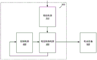
In the present application, the control circuit 400 may be provided in a voltage conversion device for controlling a voltage conversion circuit in the voltage conversion device, which may be a battery charging system or a battery management module provided in the battery charging system. As shown in fig. 9, a battery charging system 900 includes a 3-step down voltage converting circuit 100, a control circuit 400, and a voltage stabilizing circuit 910. The voltage stabilizing circuit 910 receives an ac voltage output by an external ac voltage source and converts the ac voltage into a dc voltage with a higher voltage value; the control circuit 400 outputs two pwm signals to control the on and off of the semiconductor switches in the voltage conversion circuit 100 according to the voltage signal fed back by the 3-step-down voltage conversion circuit 100; the 3-step-down voltage converting circuit 100 receives the dc voltage, and outputs a dc voltage with a lower voltage value to the battery device 920 according to the pwm signal, so as to complete the entire charging process.
The voltage converting circuit may be the 3-step-down voltage converting circuit 100, the 3-step-up voltage converting circuit 800, or other types of voltage converting circuits, which is not limited in this application. In one embodiment, the control Circuit 400 may be disposed as a discrete device on a PCB (Printed Circuit Board) or packaged in an ASIC (Application-Specific Integrated Circuit). In another embodiment, the control circuit 400 and the voltage converting circuit are disposed together as separate devices on one PCB or packaged together in one ASIC.
The above description is only for the specific embodiments of the present application, but the scope of the present application is not limited thereto, and any person skilled in the art can easily conceive of the changes or substitutions within the technical scope of the present application, and shall be covered by the scope of the present application. Therefore, the protection scope of the present application shall be subject to the protection scope of the claims.