Detailed Description
In order to make the objects, technical solutions and advantages of the present invention more apparent, the present invention is described in further detail below with reference to the accompanying drawings and embodiments. It should be understood that the specific embodiments described herein are merely illustrative of the invention and are not intended to limit the invention. In addition, the technical features involved in the embodiments of the present invention described below may be combined with each other as long as they do not conflict with each other.
As shown in fig. 3, the flexible sensor based on the multifunctional sensing principle has a three-layer structure, which can be divided into an upper electrode layer, a middle dielectric layer and a lower electrode layer, wherein the upper and lower electrodes are made of liquid metal materials, so that the tensile property of the electrode layers is improved; the intermediate dielectric layer adopts a multilayer stepped mesoporous microstructure, the elastic modulus is reduced along with the increase of the porosity of the multilayer stepped mesoporous film, the rigidity of a dielectric material is effectively reduced, the intermediate dielectric is easier to deform under the same load, the sensitivity of the sensor for pressure sensing based on a capacitance sensing principle is enhanced, and a layered stepped mesoporous structure is formed as the diameter of a stepped hole is reduced along the vertical direction, so that the thickness change rate under compression is effectively controlled, and the linearity of a capacitance change curve is improved.
The upper electrode substrate, the lower electrode substrate and the middle dielectric layer are made of flexible and stretchable high polymer materials such as PDMS, ecoflex, PI, PTFE or PET and serve as a supporting layer and a dielectric layer of the sensor. The material has good stretchability to ensure the effectiveness of the electrode in working in a stretchable state, and simultaneously has a higher relative dielectric constant as a dielectric layer, thereby ensuring a larger initial capacitance value of the sensor. The functional layers of the upper electrode and the lower electrode are used for collecting and transmitting voltage and capacitance signals, and a liquid metal material is adopted, and comprises the following components in percentage by mass: 68.5 percent of gallium, 21.5 percent of indium and 10 percent of tin, and the material has good conductive performance and tensile property. The upper electrode layer, the middle dielectric layer and the lower electrode layer of the sensor are made of stretchable materials, so that the sensor has good stretchable performance. By adjusting the process parameters, the overall thickness of the sensor can be reduced so that the sensor can be closely attached to the robot surface by van der waals forces and maintain good conformal contact.
In order to improve the success rate and the quality of the sensor, the preparation method of the flexible capacitive sensor with high sensitivity mainly comprises a multilayer stepped mesoporous microstructure process, an electrode process, a sacrificial layer process and a reactive ion etching process. The multilayer stepped mesoporous microstructure technology is used for preparing a middle dielectric layer, the electrode technology is used for preparing an upper electrode layer and a lower electrode layer, the sacrificial layer technology is used for releasing the sensor from a silicon wafer 1, and the reactive ion etching technology is used for bonding and packaging the upper electrode layer, the middle dielectric layer and the lower electrode layer. The multilayer stepped mesoporous microstructure technology adopts a centrifugal method to prepare a multilayer ordered microstructure with gradually increased pore diameters on polydimethylsiloxane. The electrode process directly injects liquid metal on the gold electrode pattern by utilizing the hydrophobicity of the liquid metal to polydimethylsiloxane and the hydrophilicity to gold, and the process method simplifies the experimental steps. The sacrificial layer process adopts polyvinyl alcohol as a material, which is an organic high polymer material dissolved in water, is colorless, transparent, nontoxic and harmless, and has good film forming property. The solvent for dissolving the polyvinyl alcohol sacrificial layer is water, so that the silicon wafer 1 and the sensor cannot be damaged, and the environment cannot be polluted. The reactive ion etching process can well bond the upper electrode layer, the middle dielectric layer and the lower electrode layer, and has high packaging strength. The method comprises the following steps:
first, upper and lower electrodes are prepared, wherein the steps (5) to (10) are photolithography
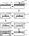
(1) Washing a clean 2-inch silicon wafer 1 by using acetone 11, isopropanol 12 and deionized water in sequence, and then drying by using nitrogen;
(2) spin-coating a sacrificial layer solution, namely a 10% polyvinyl alcohol aqueous solution, on the polished surface of the silicon wafer 1 at a spin-coating speed of 500-800 rpm for 30-60 seconds, then placing the silicon wafer 1 on a hot plate for heating at 80-100 ℃ for 5-15 minutes to evaporate water by heating, and curing the polyvinyl alcohol into a film to form a sacrificial layer 2;
(3) spin-coating polydimethylsiloxane on the silicon wafer 1 coated with the sacrificial layer 2 to serve as an underlayer 3 at a spin-coating speed of 800-1200 rpm for 50-100 s, then placing the silicon wafer 1 on a hot plate to be heated at a heating temperature of 80-100 ℃ for 10-30 min, and curing the polydimethylsiloxane to form a film so as to form a cured polydimethylsiloxane film 3;
(4) putting the silicon wafer 1 in a magnetron cavity to sputter a layer of chromium 4 and gold 5, wherein the thickness of the chromium 4 sputtered is 10-40 nm, the thickness of the gold 5 sputtered is 50-250 nm, and the chromium serves as an adhesion layer between the gold and the polydimethylsiloxane 3;
(5) spin-coating a photoresist 8 (positive photoresist) on the sputtered gold thin film, and adopting multi-step spin-coating, wherein the spin-coating speed is 500-1000 rpm, and the spin-coating time is 5-10 s; then, the spin coating speed is 1000-2500 rpm, the spin coating time is 45-80 s, and the photoresist 8 with the thickness of about 2-4 um is obtained;
(6) prebaking, volatilizing most of solvent in the photoresist, and heating the silicon wafer 1 coated with the photoresist 8 on a hot plate at 50-80 ℃ for 40-100 s;
(7) ultraviolet exposure, namely performing ultraviolet exposure under ultraviolet rays 6 under a prepared pattern of a mask plate 7 by adopting a contact type exposure technology, wherein the photoetching power is 10-20 mW/m2Setting the exposure time to be 5-10 s;
(8) developing for about 15-25 s in a special developing solution for the AZ5214 photoresist, cleaning floating glue on the surface of the gold film by using absolute ethyl alcohol, drying by using nitrogen, observing whether the electrode pattern is developed cleanly under a microscope with a super depth of field, and continuing developing until the photoresist is completely removed from the surface of the gold film if the photoresist remains;
(9) preparing a gold etching solution 9 and a chromium etching solution 10, wherein the adopted gold etching solution 9 is KI and I2Preparing etching solution 9 of gold by potassium iodide, iodine and deionized water according to the mass ratio of 6.64:1.77:60 (1.66: 0.44:60, 3.32:0.89:60 and 8.3:2.22: 60); preparing a chromium etching solution 10, and preparing the chromium etching solution 10 from ammonium ceric nitrate, glacial acetic acid and deionized water according to the proportion of 4g:1mL:20 mL;
(10) wet etching, namely soaking the silicon wafer sputtered with gold 5 and chromium 4 in gold etching solution 9 for 60-120 s, then washing the etching solution on the surface of the silicon wafer with deionized water, and drying the silicon wafer with nitrogen; then, placing the silicon wafer in a chromium etching solution 10, wherein the etching time is 30-50 s, then washing the etching solution on the surface of the silicon wafer, and drying the silicon wafer by using nitrogen to obtain a required gold electrode pattern;
(11) filling liquid metal 14 on the electrode pattern sputtered with gold 5 by using an injector in an oxygen-free glove box, wherein the thickness of the filled liquid metal 14 is 20-50 um, and sucking away redundant liquid metal by using the injector;
(12) spin coating polydimethylsiloxane again on the silicon wafer 1 subjected to the steps at the spin coating speed of 800-1000 rpm for 50-100 s, then placing the silicon wafer on a hot plate for heating at the heating temperature of 80-100 ℃ for 10-30 min, solidifying the polydimethylsiloxane into a film 2 with the thickness of 50-200 um, then placing the silicon wafer into a crystallizing dish 15 filled with deionized water for water bath heating, dissolving the polyvinyl alcohol sacrificial layer 2, and forming a polydimethylsiloxane film 13 with a liquid metal electrode to finish the preparation of the electrode layer;
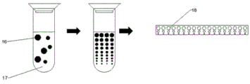
fig. 2 is a flow chart for preparing an intermediate dielectric layer, constructed in accordance with a preferred embodiment of the present invention, as shown in fig. 2.
(13) Taking 2 clean 20ml centrifuge tubes of the centrifuge tube, pouring 8 ml-12 ml of polydimethylsiloxane 17 with the same volume, adding 200 ul-500 ul of deionized water 16 by using a liquid transfer device, and stirring the mixture for 20-30 minutes to generate uniformly mixed polydimethylsiloxane/deionized water suspension;
(14) putting a centrifugal tube filled with polydimethylsiloxane/deionized water suspension into a symmetrical horizontal rotor centrifugal machine, checking whether a rotor and a cavity are clean, screwing a rotor cover, setting the centrifugal temperature to be 25 ℃ and the centrifugal force to be 3000-4000 g, screwing the rotor cover, and starting centrifugation, wherein the centrifugation time is 40-60 minutes;
(15) after centrifugation, putting the centrifuged centrifugal tube into an oven, heating at 90 ℃ for 15-20 minutes to remove deionized water and form a gap in polydimethylsiloxane;
(16) stripping the polydimethylsiloxane film 18 with the multilayer stepped mesoporous microstructure from the centrifugal tube to complete the preparation of the polydimethylsiloxane film with the multilayer stepped mesoporous microstructure;
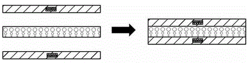
finally, the upper and lower electrode layers, the friction layer and the middle dielectric layer are packaged
(17) Adhering an upper electrode layer, a polydimethylsiloxane membrane 18 with a multilayer stepped mesoporous microstructure and a lower electrode layer together by reactive ion etching, then heating the upper electrode layer, the polydimethylsiloxane membrane and the lower electrode layer on a hot plate at the heating temperature of 80-100 ℃ for 20-30 minutes to accelerate the bonding and bonding process, wherein the reactive ion etching parameters are as follows: the flow rate of oxygen is 20 ml/min, the pressure in the reaction chamber is 70 Pa, the radio frequency power is 90W, and the reaction time is 90 seconds, thus completing the preparation of the sensor.
Preferably, the electrode material adopts gallium alloy, and the mass fractions of gallium, indium and tin are respectively 68.5%, 21.5% and 10%.
As optimization, the filling of the liquid metal is carried out in a glove box with the oxygen content less than or equal to 10 ppm.
As optimization, the upper electrode and the lower electrode are manufactured by AZ5214 photoresist, and the thickness of the photoresist is controlled to be 2 +/-0.5 microns.
As an optimization, the intermediate dielectric layer multi-layer stepped mesoporous microstructure is prepared by a centrifugal processing technology, as described in steps (13) - (16), firstly, polydimethylsiloxane and deionized water are mixed, the mass ratio of the deionized water to the polydimethylsiloxane is adjusted to obtain different pores, then the mixture is stirred, then the mixture is poured into a centrifuge tube, the centrifuge tube is centrifuged by a horizontal rotor centrifuge, then heating is carried out, and finally, the polydimethylsiloxane membrane 18 with the multi-layer stepped mesoporous microstructure is peeled off from the centrifuge tube, so that the intermediate dielectric layer is prepared.
As optimization, before the polydimethylsiloxane film is subjected to hydrophobic treatment, the polydimethylsiloxane film and oxygen are subjected to reactive ion etching.
As optimization, the distance between the upper electrode layer and the lower electrode layer is preferably 50um ~ 200um, and the thickness of upper electrode layer and lower electrode layer is preferably 100um ~ 200um, and the distance and the thickness of upper electrode layer and lower electrode layer are used for guaranteeing great electric capacity, promote sensor interference killing feature, and the thickness of middle dielectric layer is preferably 100um ~ 200um to this reduces the middle dielectric layer rigidity of sensor, promotes sensor sensitivity, guarantees sensor stability simultaneously.
Preferably, the flexible matrix material is PDMS, ecoflex, PI, PTFE or PET, so as to ensure the stretchability of the sensor.
The liquid metal is preferably gallium alloy, so as to ensure that the electrode is liquid at normal temperature, ensure the stretchability of the sensor, and simultaneously have no toxicity and are relatively safe
The present invention will be further illustrated with reference to specific examples.
Example 1:
first, upper and lower electrodes are prepared, wherein steps (5) to (10) are photolithography techniques.
(1) Cleaning the polished surface of the 2-inch silicon wafer 1 by using acetone 11, isopropanol 12 and deionized water in sequence, and then drying by using nitrogen;
(2) spin-coating 10% polyvinyl alcohol aqueous solution on the polished surface of the silicon wafer 1 at a spin-coating speed of 500 rpm for 60 seconds, then placing the silicon wafer 1 on a hot plate and heating at 80 ℃ for 15 minutes, and curing the polyvinyl alcohol to form a film to form a sacrificial layer 2;
(3) spin-coating polydimethylsiloxane on the silicon wafer 1 coated with the sacrificial layer at the spin-coating speed of 1000 rpm for 60 seconds, then placing the silicon wafer 1 on a hot plate to be heated at the heating temperature of 90 ℃ for 20 minutes, and curing the polydimethylsiloxane into a film to form a cured polydimethylsiloxane film 3;
(4) putting the silicon wafer 1 coated with the polydimethylsiloxane and the sacrificial layer in a magnetron cavity to sputter a layer of chromium 4 and gold 5, wherein the thickness of the chromium 4 sputtered is 10nm, the thickness of the gold 5 sputtered is 100nm, and the chromium serves as an adhesion layer between the gold and the polydimethylsiloxane;
(5) spin-coating AZ5214 photoresist 8 (positive photoresist) on the sputtered gold thin film, and adopting multi-step spin-coating, wherein the spin-coating speed is 500 r/min, and the spin-coating time is 8 s; then, the spin coating speed is 2500 rpm, the spin coating time is 45s, and the photoresist with the thickness of 2um is obtained;
(6) pre-baking, namely heating the silicon wafer coated with the AZ5214 photoresist 8 on a hot plate at the temperature of 60 ℃ for 60 s;
(7) ultraviolet exposure, namely performing ultraviolet 6 exposure under a prepared mask 7 pattern, wherein a contact exposure technology is adopted, the photoetching power is 15mW/m2, and the exposure time is set to be 7 s;
(8) developing to obtain a required pattern, developing for 20s in a special developing solution for AZ5214 photoresist, cleaning floating glue on the surface of the gold 5 film by using absolute ethyl alcohol, and blow-drying by using nitrogen to completely remove the photoresist from the surface of the gold 5 film;
(9) preparing a gold etching solution 9 and a chromium etching solution 10, wherein the adopted gold etching solution 9 is KI and I2Preparing etching solution 9 of gold from potassium iodide, iodine and deionized water according to the mass ratio of 6.64:1.77: 60; preparing a chromium etching solution 10, and preparing the chromium etching solution 10 from ammonium ceric nitrate, glacial acetic acid and deionized water according to the proportion of 4g:1mL:20 mL;
(10) wet etching to remove gold and chromium outside the photoresist pattern, firstly soaking the silicon wafer sputtered with gold and chromium in gold etching solution for 75s, then washing the silicon wafer surface etching solution with deionized water, and drying with nitrogen; then, the silicon wafer is placed in a chromium etching solution, the etching time is 30s, then the etching solution on the surface of the silicon wafer is washed clean, and the silicon wafer is dried by nitrogen to obtain a required gold electrode pattern;
(11) filling liquid metal 14 on the electrode pattern sputtered with gold by using an injector in an oxygen-free glove box, and sucking away redundant liquid metal by using the injector, wherein the thickness of the liquid metal 14 is about 40 micrometers;
(12) spin coating polydimethylsiloxane again on the silicon wafer 1 subjected to the steps, wherein the spin coating speed is 1000 rpm, and the spin coating time is 60 seconds, then placing the silicon wafer 1 on a hot plate to be heated, the heating temperature is 90 ℃, the heating time is 20 minutes, and the polydimethylsiloxane is cured into a film, wherein the film thickness obtained under the conditions is 100 micrometers;
second, an intermediate dielectric is prepared
(13) Taking 2 clean 20ml centrifuge tubes with centrifuge tubes, pouring 8ml polydimethylsiloxane 17, adding 200ul deionized water 16 by using a pipette, and stirring the mixture for 20 minutes to generate uniformly mixed polydimethylsiloxane/deionized water suspension;
(14) putting the centrifugal tube filled with the polydimethylsiloxane/deionized water suspension into a symmetrical horizontal rotor centrifugal machine, checking whether a rotor and a cavity are clean, screwing a rotor cover, setting the centrifugal temperature to be 25 ℃ and the centrifugal force to be 3000g, screwing the rotor cover, and starting centrifugation, wherein the centrifugation time is 40 minutes;
(15) after the centrifugation is finished, putting the centrifuged centrifugal tube into an oven, heating the centrifugal tube at 90 ℃ for 15 minutes to remove deionized water and form a gap in polydimethylsiloxane;
(16) stripping the polydimethylsiloxane film 18 with the multilayer stepped mesoporous microstructure from the centrifugal tube to complete the preparation of the polydimethylsiloxane film with the multilayer stepped mesoporous microstructure;
finally, the upper and lower electrode layers, the friction layer and the middle dielectric layer are packaged
(17) Adhering the upper electrode layer, the polydimethylsiloxane film 18 with the multilayer stepped mesopores and the lower electrode layer together by reactive ion etching, and then heating the mixture on a hot plate at the heating temperature of 80 ℃ for 30 minutes, wherein the reactive ion etching parameters are as follows: the oxygen flow is 20 ml/min, the pressure in the reaction chamber is 70 Pa, the radio frequency power is 90W, and the reaction time is 90 seconds; and accelerating the bonding and adhering process to finish the preparation of the sensor.
Example 2:
first, upper and lower electrodes are prepared, wherein steps (5) to (10) are photolithography techniques.
(1) Cleaning the polished surface of the 2-inch silicon wafer 1 by using acetone 11, isopropanol 12 and deionized water in sequence, and then drying by using nitrogen;
(2) spin-coating a 10% polyvinyl alcohol aqueous solution on the polished surface of the silicon wafer 1 at a spin-coating speed of 600 rpm for 50 seconds, then placing the silicon wafer 1 on a hot plate and heating at a heating temperature of 80 ℃ for 12 minutes to solidify the polyvinyl alcohol into a film, and forming a sacrificial layer 2;
(3) spin-coating polydimethylsiloxane on the silicon wafer 1 coated with the sacrificial layer at the speed of 900 rpm for 70 seconds, then placing the silicon wafer 1 on a hot plate for heating at the temperature of 80 ℃ for 25 minutes, and curing the polydimethylsiloxane into a film to form a cured polydimethylsiloxane film 3;
(4) putting the silicon wafer 1 coated with the polydimethylsiloxane and the sacrificial layer in a magnetron cavity, and sputtering a layer of chromium 4 and 5-gold, wherein the thickness of the chromium 4 is 20nm in a sputtering mode, the thickness of the gold 5 is 150nm in a sputtering mode, and the chromium 4 serves as an adhesion layer between the gold 5 and the polydimethylsiloxane;
(5) spin-coating AZ5214 photoresist 8 (positive photoresist) on the sputtered gold thin film, and adopting multi-step spin-coating, wherein the spin-coating speed is 800 r/min, and the spin-coating time is 5 s; then spin-coating speed is 2000 rpm, spin-coating time is 60s, and photoresist 8 with thickness of about 3um is obtained;
(6) prebaking, namely putting the silicon wafer coated with the AZ5214 photoresist 8 on a hot plate for heating at 70 ℃ for 50 seconds;
(7) ultraviolet exposure, which is ultraviolet 6 exposure under a prepared pattern of a reticle 7, herein used is a contact exposure technique, wherein the photolithography power is 20mW/m2, and the exposure time is set to 5 s;
(8) developing to obtain a required pattern, developing for 20s in a special developing solution for AZ5214 photoresist, cleaning floating glue on the surface of the gold film by absolute ethyl alcohol, and blow-drying by nitrogen to completely remove the photoresist from the surface of the gold film;
(9) preparing gold etching liquid 9 and chromium etching liquid 10, wherein the adopted gold etching liquid is KI and I2Preparing etching solution 9 of gold from potassium iodide, iodine and deionized water according to the mass ratio of 1.66:0.44: 60; preparing a chromium etching solution 10, and preparing the chromium etching solution from ammonium ceric nitrate, glacial acetic acid and deionized water according to the proportion of 4g:1mL:20 mL;
(10) wet etching to remove gold and chromium outside the photoresist pattern, firstly soaking the silicon wafer sputtered with gold and chromium in a gold etching solution for 90 seconds, then washing the silicon wafer surface etching solution with deionized water, and drying with nitrogen; then, the silicon wafer is placed in a chromium etching solution, the etching time is 35 seconds, then the etching solution on the surface of the silicon wafer is washed clean, and the silicon wafer is dried by nitrogen to obtain a required gold electrode pattern;
(11) filling the liquid metal 14 on the electrode pattern sputtered with gold by using an injector in an oxygen-free glove box, and sucking away the redundant liquid metal 14 by using the injector, wherein the thickness of the liquid metal is about 30 micrometers;
(12) spin coating polydimethylsiloxane again on the silicon wafer 1 subjected to the steps at the spin coating speed of 900 rpm for 70 seconds, then placing the silicon wafer 1 on a hot plate for heating at the heating temperature of 80 ℃ for 25 minutes, and curing the polydimethylsiloxane into a film, wherein the thickness of the obtained film is 120 micrometers;
second, an intermediate dielectric is prepared
(13) Taking 2 clean 20ml centrifuge tubes with centrifuge tubes, pouring 8ml polydimethylsiloxane, adding 300ul deionized water by using a pipette, and stirring the mixture for 25 minutes to generate uniformly mixed polydimethylsiloxane/deionized water suspension;
(14) putting the centrifugal tube filled with the polydimethylsiloxane/deionized water suspension into a symmetrical horizontal rotor centrifugal machine, checking whether a rotor and a cavity are clean, screwing a rotor cover, setting the centrifugal temperature to be 25 ℃ and the centrifugal force to be 3000g, screwing the rotor cover, and starting centrifugation, wherein the centrifugation time is 45 minutes;
(15) after the centrifugation is finished, putting the centrifuged centrifugal tube into an oven, heating the centrifugal tube at 90 ℃ for 20 minutes to remove deionized water and form a gap in polydimethylsiloxane;
(16) stripping the polydimethylsiloxane film 18 with the multilayer stepped mesoporous microstructure from the centrifugal tube to complete the preparation of the polydimethylsiloxane film with the multilayer stepped mesoporous microstructure;
finally, the upper and lower electrode layers, the friction layer and the middle dielectric layer are packaged
(17) Adhering the upper electrode layer, the polydimethylsiloxane film 18 with the multilayer stepped mesopores and the lower electrode layer together by reactive ion etching, and then heating the mixture on a hot plate at the heating temperature of 100 ℃ for 20 minutes, wherein the reactive ion etching parameters are as follows: the oxygen flow is 20 ml/min, the pressure in the reaction chamber is 70 Pa, the radio frequency power is 90W, and the reaction time is 90 seconds; and accelerating the bonding and adhering process to finish the preparation of the sensor.
Example 3:
first, upper and lower electrodes are prepared, wherein steps (5) to (10) are photolithography techniques.
(1) Cleaning the polished surface of the 2-inch silicon wafer 1 by using acetone 11, isopropanol 12 and deionized water in sequence, and then drying by using nitrogen;
(2) spin-coating a 10% polyvinyl alcohol aqueous solution on the polished surface of the silicon wafer 1 at a spin-coating speed of 800 rpm for 40 seconds, then placing the silicon wafer 1 on a hot plate and heating at a heating temperature of 80 ℃ for 15 minutes, and curing the polyvinyl alcohol to form a film to form a sacrificial layer 2;
(3) spin-coating polydimethylsiloxane on the silicon wafer 1 coated with the sacrificial layer at the spin-coating speed of 800 rpm for 80 seconds, then placing the silicon wafer 1 on a hot plate to be heated at the heating temperature of 100 ℃ for 15 minutes, and curing the polydimethylsiloxane into a film to form a cured polydimethylsiloxane film 3;
(4) putting the silicon wafer 1 coated with the polydimethylsiloxane and the sacrificial layer in a magnetron cavity, and sputtering a layer of chromium 4 and gold 5, wherein the thickness of the chromium 4 is sputtered to be 30nm, the thickness of the gold 5 is sputtered to be 50nm, and the chromium 4 serves as an adhesion layer between the gold 5 and the polydimethylsiloxane;
(5) spin-coating AZ5214 photoresist 8 (positive photoresist) on the sputtered gold 4 film, and adopting multi-step spin-coating, wherein the spin-coating speed is 600 revolutions per minute, and the spin-coating time is 7 s; then, the spin coating speed is 1500 rpm, the spin coating time is 70s, and the photoresist 8 with the thickness of 3.5um is obtained;
(6) pre-baking, namely heating the silicon wafer coated with the AZ5214 photoresist 8 on a hot plate for 100s at the temperature of 50 ℃;
(7) ultraviolet exposure, namely performing ultraviolet 6 exposure under a prepared mask 7 pattern, wherein a contact exposure technology is adopted, the photoetching power is 10mW/m2, and the exposure time is set to be 10 s;
(8) developing to obtain a required pattern, developing for 25s in a special developing solution for AZ5214 photoresist, cleaning floating glue on the surface of the gold film by absolute ethyl alcohol, and blow-drying by nitrogen to completely remove the photoresist 8 from the surface of the gold film;
(9) preparing gold etching liquid 9 and chromium etching liquid 10, wherein the adopted gold etching liquid is KI and I2Preparing etching solution 9 of gold from potassium iodide, iodine and deionized water according to the mass ratio of 3.32:0.89: 60; preparing a chromium etching solution 10, and preparing the chromium etching solution 10 from ammonium ceric nitrate, glacial acetic acid and deionized water according to the proportion of 4g:1mL:20 mL;
(10) wet etching, namely removing gold 5 and chromium 4 outside the photoresist pattern, firstly soaking the silicon wafer sputtered with the gold 5 and the chromium 4 in gold etching solution for 60s, then washing the etching solution on the surface of the silicon wafer with deionized water, and drying the silicon wafer with nitrogen; then, the silicon wafer is placed in a chromium etching solution, the etching time is 40s, then the etching solution on the surface of the silicon wafer is washed clean, and the silicon wafer is dried by nitrogen to obtain a required gold electrode pattern;
(11) filling the liquid metal 14 on the electrode pattern sputtered with gold by using an injector in an oxygen-free glove box, and sucking away the redundant liquid metal 14 by using the injector, wherein the thickness of the liquid metal is about 25 micrometers;
(12) spin coating polydimethylsiloxane again on the silicon wafer 1 subjected to the steps, wherein the spin coating speed is 800 revolutions per minute and the spin coating time is 80 seconds, then placing the silicon wafer 1 on a hot plate to be heated, the heating temperature is 100 ℃, the heating time is 15 minutes, and the polydimethylsiloxane is solidified into a film, wherein the film thickness obtained under the conditions is 110 micrometers;
second, an intermediate dielectric is prepared
(13) Taking 2 clean 20ml centrifuge tubes of the centrifuge tube, pouring 10ml polydimethylsiloxane 17, adding 400ul deionized water 16 by using a pipette, and stirring the mixture for 30 minutes to generate uniformly mixed polydimethylsiloxane/deionized water suspension;
(14) putting the centrifugal tube filled with the polydimethylsiloxane/deionized water suspension into a symmetrical horizontal rotor centrifugal machine, checking whether a rotor and a cavity are clean, screwing a rotor cover, setting the centrifugal temperature to be 25 ℃ and the centrifugal force to be 3000g, screwing the rotor cover, and starting centrifugation, wherein the centrifugation time is 40 minutes;
(15) after the centrifugation is finished, putting the centrifuged centrifugal tube into an oven, heating the centrifugal tube at 90 ℃ for 15 minutes to remove deionized water and form a gap in polydimethylsiloxane;
(16) stripping the polydimethylsiloxane film 18 with the multilayer stepped mesoporous microstructure from the centrifugal tube to complete the preparation of the polydimethylsiloxane film with the multilayer stepped mesoporous microstructure;
finally, the upper and lower electrode layers, the friction layer and the middle dielectric layer are packaged
(17) Adhering the upper electrode layer, the polydimethylsiloxane film 18 with the multilayer stepped mesopores and the lower electrode layer together by reactive ion etching, and then heating the mixture on a hot plate at the heating temperature of 80 ℃ for 30 minutes, wherein the reactive ion etching parameters are as follows: the oxygen flow is 20 ml/min, the pressure in the reaction chamber is 70 Pa, the radio frequency power is 90W, and the reaction time is 90 seconds; and accelerating the bonding and adhering process to finish the preparation of the sensor.
Example 4:
first, upper and lower electrodes are prepared, wherein steps (5) to (10) are photolithography techniques.
(1) Cleaning the polished surface of the 2-inch silicon wafer 1 by using acetone 11, isopropanol 12 and deionized water in sequence, and then drying by using nitrogen;
(2) spin-coating a 10% polyvinyl alcohol aqueous solution on the polished surface of the silicon wafer 1 at a spin-coating speed of 700 rpm for 45 seconds, then placing the silicon wafer 1 on a hot plate to be heated at a heating temperature of 90 ℃ for 10 minutes, and curing the polyvinyl alcohol to form a film to form a sacrificial layer 2;
(3) spin-coating polydimethylsiloxane on the silicon wafer 1 coated with the sacrificial layer at the spin-coating speed of 1200 rpm for 50 seconds, then placing the silicon wafer 1 on a hot plate for heating at the heating temperature of 95 ℃ for 18 minutes, and curing the polydimethylsiloxane into a film to form a cured polydimethylsiloxane film 3;
(4) putting the silicon wafer 1 coated with the polydimethylsiloxane and the sacrificial layer in a magnetron cavity, and sputtering a layer of chromium 4 and gold 5, wherein the thickness of the chromium 4 is 40nm in a sputtering mode, the thickness of the gold 5 is 200nm in a sputtering mode, and the chromium 4 serves as an adhesion layer between the gold 5 and the polydimethylsiloxane;
(5) spin-coating AZ5214 photoresist 8 (positive photoresist) on the sputtered gold 4 film, and adopting multi-step spin-coating, wherein the spin-coating speed is 700 r/min, and the spin-coating time is 6 s; then spin-coating at a speed of 1000 rpm for 80s to obtain a photoresist with a thickness of 4 um;
(6) pre-baking, namely heating the silicon wafer coated with the AZ5214 photoresist 8 on a hot plate at the temperature of 80 ℃ for 40 s;
(7) ultraviolet exposure, namely performing ultraviolet 6 exposure under a prepared mask 7 pattern, wherein a contact exposure technology is adopted, the photoetching power is 15mW/m2, and the exposure time is set to be 7 s;
(8) developing to obtain a required pattern, developing for 20s in a special developing solution for AZ5214 photoresist, cleaning floating glue on the surface of the gold thin film 4 by using absolute ethyl alcohol, and blow-drying by using nitrogen to completely remove the photoresist 8 from the surface of the gold thin film 4;
(9) preparing a gold etching solution 9 and a chromium etching solution 10, wherein the adopted gold etching solution 9 is KI and I2Preparing etching solution 9 of gold from potassium iodide, iodine and deionized water according to the mass ratio of 8.3:2.22: 60; preparing a chromium etching solution 10, and preparing the chromium etching solution 10 from ammonium ceric nitrate, glacial acetic acid and deionized water according to the proportion of 4g:1mL:20 mL;
(10) wet etching, namely removing gold 5 and chromium 4 outside the photoresist pattern, firstly soaking the silicon wafer sputtered with the gold 5 and the chromium 4 in gold etching solution 10 for 120s, then washing the etching solution on the surface of the silicon wafer with deionized water, and drying the silicon wafer with nitrogen; then, the silicon wafer is placed in a chromium etching solution 9, the etching time is 50s, then the etching solution on the surface of the silicon wafer is washed clean, and the silicon wafer is dried by nitrogen to obtain a required gold electrode pattern;
(11) filling liquid metal 14 on the electrode pattern sputtered with gold by using an injector in an oxygen-free glove box, and sucking away redundant liquid metal by using the injector, wherein the thickness of the liquid metal 14 is about 20 microns;
(12) spin-coating polydimethylsiloxane again on the silicon wafer 1 subjected to the steps at the spin-coating speed of 1200 rpm for 50 seconds, then placing the silicon wafer 1 on a hot plate for heating at the heating temperature of 95 ℃ for 18 minutes, and curing the polydimethylsiloxane into a film, wherein the thickness of the film obtained under the conditions is 90 micrometers;
second, an intermediate dielectric is prepared
(13) Taking 2 clean 20ml centrifuge tubes of the centrifuge tube, pouring 10ml polydimethylsiloxane 17, adding 500ul deionized water 16 by using a pipette, and stirring the mixture for 30 minutes to generate uniformly mixed polydimethylsiloxane/deionized water suspension;
(14) putting the centrifugal tube filled with the polydimethylsiloxane/deionized water suspension into a symmetrical horizontal rotor centrifugal machine, checking whether a rotor and a cavity are clean, screwing a rotor cover, setting the centrifugal temperature to be 25 ℃ and the centrifugal force to be 4000g, screwing the rotor cover, and starting centrifugation, wherein the centrifugation time is 50 minutes;
(15) after the centrifugation is finished, putting the centrifuged centrifugal tube into an oven, heating the centrifugal tube at 90 ℃ for 20 minutes to remove deionized water and form a gap in polydimethylsiloxane;
(16) stripping the polydimethylsiloxane film 18 with the multilayer stepped mesoporous microstructure from the centrifugal tube to complete the preparation of the polydimethylsiloxane film with the multilayer stepped mesoporous microstructure;
finally, the upper and lower electrode layers, the friction layer and the middle dielectric layer are packaged
(17) Adhering the upper electrode layer, the polydimethylsiloxane film 18 with the multilayer stepped mesopores and the lower electrode layer together by reactive ion etching, and then heating the mixture on a hot plate at the heating temperature of 90 ℃ for 25 minutes, wherein the reactive ion etching parameters are as follows: the oxygen flow is 20 ml/min, the pressure in the reaction chamber is 70 Pa, the radio frequency power is 90W, and the reaction time is 90 seconds; and accelerating the bonding and adhering process to finish the preparation of the sensor.
It will be understood by those skilled in the art that the foregoing is only a preferred embodiment of the present invention, and is not intended to limit the invention, and that any modification, equivalent replacement, or improvement made within the spirit and principle of the present invention should be included in the scope of the present invention.