Disclosure of Invention
In order to overcome the defects and shortcomings of the prior art, the invention provides a wireless energy transmission system and method based on vector power superposition, and solves the problems of a single electric field coupling or magnetic field coupling mode in the aspects of power, flexibility, interference resistance and the like.
The invention adopts the following technical scheme:
a wireless energy transmission system based on vector power superposition comprises a power supply circuit, a clock control and gate drive circuit, a first inverter circuit, a second inverter circuit, a wireless energy coupling circuit and an AC-DC conversion circuit;
the output end of the power supply circuit is respectively connected with the power supply input ends of the first inverter circuit and the second inverter circuit to provide stable direct-current voltage;
the clock control and grid electrode driving circuit is provided with two output ends which are respectively connected with the signal input ends of the first inverter circuit and the second inverter circuit and output grid electrode control signals;
the first output end and the second output end of the first inverter circuit are respectively connected with the first input end and the second input end of the wireless energy coupling circuit, and convert the direct-current voltage output by the power supply into alternating-current voltage to provide transmitting power for the wireless energy coupling circuit;
the first output end and the second output end of the second inverter circuit are respectively connected with the third input end and the fourth input end of the wireless energy coupling circuit;
the first output end and the second output end of the wireless energy coupling circuit are respectively connected with the first input end and the second input end of the AC-DC conversion circuit;
and the output end of the AC-DC conversion circuit is connected with a load.
The wireless energy coupling circuit includes a primary coupling circuit and a secondary coupling circuit.
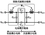
The primary coupling circuit comprises a primary transmitting coil and a primary coupling capacitor plate;
the primary transmitting coil comprises a first transmitting coil and a second transmitting coil;
the primary coupling capacitor polar plate comprises a first polar plate, a second polar plate and a third polar plate, one end of the first transmitting coil is used as a second input end of the wireless energy coupling circuit, the other end of the first transmitting coil is connected with the first polar plate, one end of the second transmitting coil is used as a third input end of the wireless energy coupling circuit, and the other end of the second transmitting coil is connected with the second polar plate;
one end of the third polar plate is a first input end of the wireless coupling circuit, and the other end of the third polar plate is a fourth input end of the wireless coupling circuit.
The secondary coupling circuit comprises a secondary receiving coil and a secondary coupling capacitor plate;
the secondary coupling capacitor polar plate comprises a fourth polar plate and a fifth polar plate, and the fourth polar plate is connected with one end of the secondary receiving coil to be used as a first output end of the wireless energy coupling circuit; and the fifth polar plate and the other end of the secondary receiving coil are connected to be used as a second output end of the wireless energy coupling circuit.
The first polar plate and the second polar plate respectively form coupling capacitors with the fourth polar plate, the second polar plate and the third polar plate form coupling capacitors, and energy transmission is carried out by utilizing electric field coupling;
and the capacitor between the first polar plate and the third polar plate, the capacitor between the second polar plate and the third polar plate, and the capacitor between the fourth polar plate and the fifth polar plate respectively form a primary side resonance circuit and a secondary side resonance circuit with the first transmitting coil, the second transmitting coil and the secondary receiving coil.
The invention transfers energy from the primary coupling circuit to the secondary coupling circuit by means of electric field coupling and magnetic field coupling.
A method for a vector power superposition based wireless energy transfer system, comprising the steps of:
the power supply circuit outputs a direct current circuit to the first inverter circuit and the second inverter circuit, and the first inverter circuit and the second inverter circuit receive grid control signals of different phases of the clock control and grid drive circuit, generate power signals of different phases and output the power signals to the wireless energy coupling circuit;
the power signals with different phases generate coupling magnetic fields and coupling electric fields with different phases at the transmitting coil and the coupling capacitor, energy in the coupling magnetic fields is received at the secondary receiving coil and the secondary coupling capacitor plate in a vector superposition mode, and the received energy is converted into direct current through the AC-DC conversion circuit to be output to the load.
The vector superposition specifically comprises: the first inverter circuit, the first transmitting coil, the first polar plate and the third polar plate form a first transmitting circuit; the second inverter circuit, the second transmitting coil, the second polar plate and the third polar plate form a second transmitting circuit; the first transmitting circuit and the second transmitting circuit transmit coupling electric fields and magnetic fields of different phases due to gate control signals of different phases generated by the clock control circuit, and are received in the secondary receiving coil and the secondary coupling plate in a vector superposition manner.
The method comprises two functional links, wherein the transmission of the functional link I is specifically as follows: the first polar plate and the fourth polar plate form a pair of coupling capacitors, the third polar plate and the fifth polar plate form a pair of coupling capacitors, and the two pairs of capacitor polar plates are mutually coupled to carry out energy transmission through an electric field;
meanwhile, an equivalent capacitor is formed between the first polar plate and the third polar plate, an equivalent capacitor is formed between the fifth polar plate and the fourth polar plate, the first transmitting coil and the equivalent capacitor form a transmitting resonant circuit, the secondary receiving coil and the equivalent capacitor form a receiving resonant circuit, and energy transmission is carried out through magnetic field coupling.
The transmission of the energy link two is specifically as follows: the second pole plate and the fourth pole plate form a pair of coupling capacitors, the third pole plate and the fifth pole plate form a pair of coupling capacitors, the two pairs of capacitor pole plates are mutually coupled to carry out energy transmission through an electric field, an equivalent capacitor is formed between the second pole plate and the third pole plate, an equivalent capacitor is formed between the third pole plate and the fourth pole plate, the second transmitting coil and the equivalent capacitor form a transmitting resonant circuit, and the secondary receiving coil and the equivalent capacitor form a receiving resonant circuit and carry out energy transmission through magnetic field coupling.
The invention has the beneficial effects that:
the invention meets the requirements on flexibility and power in wireless energy transmission; energy signals with different phases generated by the double-energy link are superposed on a receiving coil and a coupling capacitor polar plate of the receiving circuit by a vector power superposition method, so that the aim of improving and controlling transmission power is fulfilled; and due to the interaction between the coupling polar plates, the coupling polar plates not only transmit energy through electric field coupling in the transmission process, but also form a resonance circuit by using the capacitance formed between the polar plates as a resonance capacitance and a coil, thereby reducing the use of external elements and increasing the flexibility of the positions of a transmitting circuit and a receiving circuit.
Detailed Description
The present invention will be described in further detail with reference to examples and drawings, but the present invention is not limited to these examples.
Examples
The invention supplies power to the coupling circuit through the double energy links simultaneously, so that the primary transmitting circuit generates two electromagnetic fields with a certain phase difference, the electromagnetic fields excited by the double energy links are superposed in the space and then received in the coupling receiving circuit, and the energy is transmitted to the AC-DC conversion circuit, thereby realizing the superposition of the energy in the transmission process, improving the transmission power, simultaneously leading the position space of the coupling transmitting circuit and the coupling receiving circuit to have great flexibility due to the electromagnetic field coupling transmission, leading the equivalent capacitance between the capacitance plates to generate resonance with the coil when the capacitance plates are used as the coupling capacitance to transmit the energy, and further improving the position flexibility of the coupling transmitting circuit and the coupling receiving circuit. The wireless energy transmission system of the present invention will be described with reference to the accompanying drawings
As shown in fig. 1 to 6, a wireless energy transmission system based on vector power superposition includes a power circuit 101, a first inverter circuit 111, a second inverter circuit 121, a clock control and gate driving circuit 102, a wireless energy coupling circuit 131, an AC-DC conversion circuit 141, and a load 151;
the output end of the power circuit is connected with the power input ends of the first inverter circuit 111 and the second inverter circuit 121 respectively to provide stable direct-current voltage.
A first output end of the clock control and gate drive circuit 102 is connected to a signal input end of the first inverter circuit 111, and a second output end of the clock control and gate drive circuit 102 is connected to a signal input end of the second inverter circuit 121, and outputs a gate control signal to the first inverter circuit 111 and the second inverter circuit 121.
The first output end and the second output end of the first inverter circuit 111 are respectively connected with the first input end and the second input end of the wireless energy coupling circuit 131, and convert the direct-current voltage output by the power supply into alternating-current voltage to provide transmitting power for the wireless energy coupling circuit;
a first output end and a second output end of the second inverter circuit 121 are respectively connected with a third input end and a fourth input end of the wireless energy coupling circuit;
a first output end and a second output end of the wireless energy coupling circuit 131 are respectively connected with a first input end and a second input end of the AC-DC conversion circuit;
the output terminal of the AC-DC conversion circuit 141 is connected to a load 151 and converts an alternating current voltage into a direct current voltage to supply to the load.
The wireless energy coupling circuit includes a primary coupling circuit and a secondary coupling circuit.
The primary coupling circuit comprises a primary transmitting coil and a primary coupling capacitor plate;
the primary transmission coil comprises a first transmission coil L11a and a second transmission coil L12 a;
the primary coupling capacitor polar plate comprises a first polar plate I11a, a second polar plate I12a and a third polar plate I2a, one end of the first transmitting coil L11a is used as a second input end of the wireless energy coupling circuit, the other end of the first transmitting coil L11a is connected with the first polar plate, one end of the second transmitting coil L12a is used as a third input end of the wireless energy coupling circuit, and the other end of the second transmitting coil L12a is connected with the second polar plate I12 a;
one end of the third polar plate I2a is a first input end of the wireless coupling circuit, and the other end is a fourth input end of the wireless coupling circuit.
The secondary coupling circuit comprises a secondary receiving coil L2b and a secondary coupling capacitor plate;
the secondary coupling capacitor plate comprises a fourth plate I1b and a fifth plate I2b, and the fourth plate I1b is connected with one end of the secondary receiving coil to be used as a first output end of the wireless energy coupling circuit; and the fifth polar plate and the other end of the secondary receiving coil are connected to be used as a second output end of the wireless energy coupling circuit.
The first emitting coil L11a is connected with the second output end of the first inverter circuit 111, and inputs energy to the wireless energy coupling circuit as the input end of the energy link I, and the other end is connected with the first polar plate I11 a; the second transmitting coil L12a is connected to the second output terminal of the second inverter circuit 121, and inputs energy to the wireless energy coupling circuit as the input terminal of the energy link two, and the other terminal is connected to the second plate I12 a; the two ends of the third pole plate I2a are connected with the first inverter circuit 111 and the second inverter circuit 121 to be grounded.
The first polar plate and the second polar plate respectively form coupling capacitors with the fourth polar plate, the second polar plate and the third polar plate form coupling capacitors, and energy transmission is carried out by utilizing electric field coupling;
and the capacitor between the first polar plate and the third polar plate, the capacitor between the second polar plate and the third polar plate, and the capacitor between the fourth polar plate and the fifth polar plate respectively form a primary side resonance circuit and a secondary side resonance circuit with the first transmitting coil, the second transmitting coil and the secondary receiving coil.
Energy is transferred from the primary coupling circuit to the secondary coupling circuit by means of electric and magnetic field coupling.
In fig. 1, energy is transmitted to a transmitting coil and a coupling capacitor through two energy links at a transmitting end, in an inverter circuit 111, a direct current circuit from a power circuit 102 is controlled by a gate control signal of a clock control circuit 102 to generate alternating current signals with different phases, the alternating current signals with different phases generate different magnetic fields and electric fields through the transmitting coil and a coupling plate, the magnetic fields and the electric fields are overlapped in space, the energy is transmitted to a receiving end through a receiving coil and a secondary coupling plate, the receiving end processes the received alternating current through an AC-DC conversion circuit 141, and the direct current is finally output to a load.
As shown in fig. 7, the energy transmission method of the present invention specifically includes:
the power supply circuit outputs a direct current circuit to the first inverter circuit and the second inverter circuit, and the first inverter circuit and the second inverter circuit receive grid control signals of different phases of the clock control and grid drive circuit, generate power signals of different phases and output the power signals to the wireless energy coupling circuit;
the power signals with different phases generate coupling magnetic fields and coupling electric fields with different phases at the transmitting coil and the coupling capacitor, energy in the coupling magnetic fields is received at the secondary receiving coil and the secondary coupling capacitor plate in a vector superposition mode, and the received energy is converted into direct current through the AC-DC conversion circuit to be output to the load.
The method comprises two functional links, wherein the transmission of the functional link I is specifically as follows: the first polar plate I11a and the fourth polar plate I1b form a pair of coupling capacitors C11, meanwhile, the third polar plate I2a and the fifth polar plate I2b form a pair of coupling capacitors C12, and the two pairs of capacitor polar plates are coupled with each other to carry out energy transmission through an electric field;
meanwhile, an equivalent capacitor C21 is formed between the first polar plate I11a and the third polar plate I2a, an equivalent capacitor C22 is formed between the fifth polar plate I2b and the fourth polar plate I1b, the first transmitting coil L11a and the equivalent capacitor C11 form a transmitting resonant circuit, the secondary receiving coil L2b and the equivalent capacitor C22 form a receiving resonant circuit, and energy is transmitted through magnetic field coupling.
The transmission of the energy link two is specifically as follows: the second plate I12a and the fourth plate I1b form a pair of coupling capacitors C11, the third plate I2a and the fifth plate I2b form a pair of coupling capacitors C12, the two pairs of capacitor plates are coupled with each other to perform energy transmission through an electric field, an equivalent capacitor C21 is formed between the second plate I12a and the third plate I2a, an equivalent capacitor C22 is formed between the third plate I2b and the fourth plate I1b, the second transmitting coil L12a and the equivalent capacitor C11 form a transmitting resonant circuit, the secondary receiving lower face pinches off the L2b and the equivalent capacitor C22 to form a receiving resonant circuit, and energy transmission is performed through magnetic field coupling.
The vector superposition specifically comprises: the inverter circuits in the first energy link and the second energy link receive the grid control signals of the clock control circuit, and the power output by the first inverter circuit and the power output by the second inverter circuit are different in phase due to the difference in phase of the grid control signals output by the clock control and grid driving circuit, so that the electromagnetic fields generated by the first energy link and the second energy link are different; the different electromagnetic fields are superposed in space, and finally the power P1 of the energy link I and the power P2 of the energy link II are superposed in a vector superposition mode at the receiving end, and the power P12 is transmitted to the AC-DC conversion circuit and output to a load.
As shown in fig. 4, in the present embodiment, the first inverter circuit and the second inverter circuit adopt a push-pull inverter circuit, which is composed of two inductors, two MOS transistors, and two buffers; one end of an inductor LS1 is connected with a drain of a MOS tube S1, the other end of the inductor LS1 is connected to a power input end, one end of an inductor LS2 is connected with a drain of a MOS tube S2, the other end of the inductor LS1 is connected with one end of an inductor LS 3838, a source of the MOS tube S1 is connected with a source of a MOS tube S2 and grounded, a grid of the MOS tube S1 is connected with one end of a buffer INV1 composed of multi-stage inverters, the other end of the buffer INV1 is connected with a signal input end, a grid of the MOS tube S2 is connected with one end of a buffer INV2 composed of multi-stage inverters, and the other end of the buffer INV2 is connected with the signal input end.
As shown in fig. 5, the clock control and gate driving circuit includes a power supply circuit, a clock generating circuit, a frequency dividing circuit, and a delay circuit;
the power supply circuit supplies power to each unit of the circuit;
the output end of the clock generating circuit is connected with the input end of the frequency dividing circuit and outputs a clock signal to the frequency dividing circuit;
the signal input end of the frequency division circuit is connected with the output end of the clock transmitting circuit, the output end of the frequency division circuit is connected with the input end of the delay circuit, and the frequency of the clock signal is adjusted to be the required clock frequency and output to the delay circuit;
the input end of the delay circuit is connected with the input end of the frequency dividing circuit and outputs a delay signal;
the frequency dividing circuit receives a clock signal generated by the clock generating circuit, performs frequency dividing processing on the clock signal, outputs the signal to the delay circuit, and the delay circuit performs further delay processing on the signal, generates gate control signals with different phases and outputs the gate control signals to the inverter circuit.
The invention adopts a vector power superposition method, different phases generated by a clock control circuit are transmitted to a wireless energy coupling circuit through a double-energy link, different electromagnetic fields generated by the wireless energy coupling circuit are superposed in a certain space, the superposed electromagnetic field energy is transmitted to a secondary coupling circuit, the power vector superposition of the double-energy link is realized, and the coupling circuit is not easily interfered by metal foreign matters compared with independent magnetic field coupling and is more flexible in position due to the adoption of an electromagnetic field coupling mode.
The above embodiments are preferred embodiments of the present invention, but the present invention is not limited to the above embodiments, and any other changes, modifications, substitutions, combinations, and simplifications which do not depart from the spirit and principle of the present invention should be construed as equivalents thereof, and all such changes, modifications, substitutions, combinations, and simplifications are intended to be included in the scope of the present invention.