CN108806603B - Organic light-emitting display panel, driving method thereof and organic light-emitting display device - Google Patents
Organic light-emitting display panel, driving method thereof and organic light-emitting display device Download PDFInfo
- Publication number
- CN108806603B CN108806603B CN201810697105.5A CN201810697105A CN108806603B CN 108806603 B CN108806603 B CN 108806603B CN 201810697105 A CN201810697105 A CN 201810697105A CN 108806603 B CN108806603 B CN 108806603B
- Authority
- CN
- China
- Prior art keywords
- organic light
- emission
- area
- driving circuit
- row
- Prior art date
- Legal status (The legal status is an assumption and is not a legal conclusion. Google has not performed a legal analysis and makes no representation as to the accuracy of the status listed.)
- Active
Links
Images


Classifications
-
- G—PHYSICS
- G09—EDUCATION; CRYPTOGRAPHY; DISPLAY; ADVERTISING; SEALS
- G09G—ARRANGEMENTS OR CIRCUITS FOR CONTROL OF INDICATING DEVICES USING STATIC MEANS TO PRESENT VARIABLE INFORMATION
- G09G3/00—Control arrangements or circuits, of interest only in connection with visual indicators other than cathode-ray tubes
- G09G3/20—Control arrangements or circuits, of interest only in connection with visual indicators other than cathode-ray tubes for presentation of an assembly of a number of characters, e.g. a page, by composing the assembly by combination of individual elements arranged in a matrix no fixed position being assigned to or needed to be assigned to the individual characters or partial characters
- G09G3/22—Control arrangements or circuits, of interest only in connection with visual indicators other than cathode-ray tubes for presentation of an assembly of a number of characters, e.g. a page, by composing the assembly by combination of individual elements arranged in a matrix no fixed position being assigned to or needed to be assigned to the individual characters or partial characters using controlled light sources
- G09G3/30—Control arrangements or circuits, of interest only in connection with visual indicators other than cathode-ray tubes for presentation of an assembly of a number of characters, e.g. a page, by composing the assembly by combination of individual elements arranged in a matrix no fixed position being assigned to or needed to be assigned to the individual characters or partial characters using controlled light sources using electroluminescent panels
- G09G3/32—Control arrangements or circuits, of interest only in connection with visual indicators other than cathode-ray tubes for presentation of an assembly of a number of characters, e.g. a page, by composing the assembly by combination of individual elements arranged in a matrix no fixed position being assigned to or needed to be assigned to the individual characters or partial characters using controlled light sources using electroluminescent panels semiconductive, e.g. using light-emitting diodes [LED]
- G09G3/3208—Control arrangements or circuits, of interest only in connection with visual indicators other than cathode-ray tubes for presentation of an assembly of a number of characters, e.g. a page, by composing the assembly by combination of individual elements arranged in a matrix no fixed position being assigned to or needed to be assigned to the individual characters or partial characters using controlled light sources using electroluminescent panels semiconductive, e.g. using light-emitting diodes [LED] organic, e.g. using organic light-emitting diodes [OLED]
- G09G3/3225—Control arrangements or circuits, of interest only in connection with visual indicators other than cathode-ray tubes for presentation of an assembly of a number of characters, e.g. a page, by composing the assembly by combination of individual elements arranged in a matrix no fixed position being assigned to or needed to be assigned to the individual characters or partial characters using controlled light sources using electroluminescent panels semiconductive, e.g. using light-emitting diodes [LED] organic, e.g. using organic light-emitting diodes [OLED] using an active matrix
-
- G—PHYSICS
- G06—COMPUTING OR CALCULATING; COUNTING
- G06V—IMAGE OR VIDEO RECOGNITION OR UNDERSTANDING
- G06V40/00—Recognition of biometric, human-related or animal-related patterns in image or video data
- G06V40/10—Human or animal bodies, e.g. vehicle occupants or pedestrians; Body parts, e.g. hands
- G06V40/12—Fingerprints or palmprints
- G06V40/13—Sensors therefor
- G06V40/1306—Sensors therefor non-optical, e.g. ultrasonic or capacitive sensing
-
- G—PHYSICS
- G06—COMPUTING OR CALCULATING; COUNTING
- G06V—IMAGE OR VIDEO RECOGNITION OR UNDERSTANDING
- G06V40/00—Recognition of biometric, human-related or animal-related patterns in image or video data
- G06V40/10—Human or animal bodies, e.g. vehicle occupants or pedestrians; Body parts, e.g. hands
- G06V40/12—Fingerprints or palmprints
- G06V40/13—Sensors therefor
- G06V40/1318—Sensors therefor using electro-optical elements or layers, e.g. electroluminescent sensing
-
- G—PHYSICS
- G09—EDUCATION; CRYPTOGRAPHY; DISPLAY; ADVERTISING; SEALS
- G09G—ARRANGEMENTS OR CIRCUITS FOR CONTROL OF INDICATING DEVICES USING STATIC MEANS TO PRESENT VARIABLE INFORMATION
- G09G3/00—Control arrangements or circuits, of interest only in connection with visual indicators other than cathode-ray tubes
- G09G3/20—Control arrangements or circuits, of interest only in connection with visual indicators other than cathode-ray tubes for presentation of an assembly of a number of characters, e.g. a page, by composing the assembly by combination of individual elements arranged in a matrix no fixed position being assigned to or needed to be assigned to the individual characters or partial characters
- G09G3/22—Control arrangements or circuits, of interest only in connection with visual indicators other than cathode-ray tubes for presentation of an assembly of a number of characters, e.g. a page, by composing the assembly by combination of individual elements arranged in a matrix no fixed position being assigned to or needed to be assigned to the individual characters or partial characters using controlled light sources
- G09G3/30—Control arrangements or circuits, of interest only in connection with visual indicators other than cathode-ray tubes for presentation of an assembly of a number of characters, e.g. a page, by composing the assembly by combination of individual elements arranged in a matrix no fixed position being assigned to or needed to be assigned to the individual characters or partial characters using controlled light sources using electroluminescent panels
- G09G3/32—Control arrangements or circuits, of interest only in connection with visual indicators other than cathode-ray tubes for presentation of an assembly of a number of characters, e.g. a page, by composing the assembly by combination of individual elements arranged in a matrix no fixed position being assigned to or needed to be assigned to the individual characters or partial characters using controlled light sources using electroluminescent panels semiconductive, e.g. using light-emitting diodes [LED]
- G09G3/3208—Control arrangements or circuits, of interest only in connection with visual indicators other than cathode-ray tubes for presentation of an assembly of a number of characters, e.g. a page, by composing the assembly by combination of individual elements arranged in a matrix no fixed position being assigned to or needed to be assigned to the individual characters or partial characters using controlled light sources using electroluminescent panels semiconductive, e.g. using light-emitting diodes [LED] organic, e.g. using organic light-emitting diodes [OLED]
- G09G3/3266—Details of drivers for scan electrodes
-
- G—PHYSICS
- G09—EDUCATION; CRYPTOGRAPHY; DISPLAY; ADVERTISING; SEALS
- G09G—ARRANGEMENTS OR CIRCUITS FOR CONTROL OF INDICATING DEVICES USING STATIC MEANS TO PRESENT VARIABLE INFORMATION
- G09G2300/00—Aspects of the constitution of display devices
- G09G2300/04—Structural and physical details of display devices
- G09G2300/0421—Structural details of the set of electrodes
- G09G2300/0426—Layout of electrodes and connections
-
- G—PHYSICS
- G09—EDUCATION; CRYPTOGRAPHY; DISPLAY; ADVERTISING; SEALS
- G09G—ARRANGEMENTS OR CIRCUITS FOR CONTROL OF INDICATING DEVICES USING STATIC MEANS TO PRESENT VARIABLE INFORMATION
- G09G2310/00—Command of the display device
- G09G2310/02—Addressing, scanning or driving the display screen or processing steps related thereto
- G09G2310/0264—Details of driving circuits
- G09G2310/0286—Details of a shift registers arranged for use in a driving circuit
-
- G—PHYSICS
- G09—EDUCATION; CRYPTOGRAPHY; DISPLAY; ADVERTISING; SEALS
- G09G—ARRANGEMENTS OR CIRCUITS FOR CONTROL OF INDICATING DEVICES USING STATIC MEANS TO PRESENT VARIABLE INFORMATION
- G09G2320/00—Control of display operating conditions
- G09G2320/02—Improving the quality of display appearance
- G09G2320/0233—Improving the luminance or brightness uniformity across the screen
-
- G—PHYSICS
- G09—EDUCATION; CRYPTOGRAPHY; DISPLAY; ADVERTISING; SEALS
- G09G—ARRANGEMENTS OR CIRCUITS FOR CONTROL OF INDICATING DEVICES USING STATIC MEANS TO PRESENT VARIABLE INFORMATION
- G09G2320/00—Control of display operating conditions
- G09G2320/06—Adjustment of display parameters
- G09G2320/0686—Adjustment of display parameters with two or more screen areas displaying information with different brightness or colours
Landscapes
- Engineering & Computer Science (AREA)
- Physics & Mathematics (AREA)
- General Physics & Mathematics (AREA)
- Theoretical Computer Science (AREA)
- Computer Hardware Design (AREA)
- Human Computer Interaction (AREA)
- Multimedia (AREA)
- Electroluminescent Light Sources (AREA)
- Control Of Indicators Other Than Cathode Ray Tubes (AREA)
- Control Of El Displays (AREA)
Abstract
本发明实施例提供一种有机发光显示面板及其驱动方法、有机发光显示装置,涉及显示技术领域。该有机发光显示面板中,衬底基板包括显示区域和周边区域,显示区域包括常规显示子区域和指纹识别子区域;多个有机发光器件和多个像素驱动电路位于显示区域内,有机发光器件与像素驱动电路一一对应电连接;第一发射驱动电路设置于周边区域内,且与常规显示子区域内的多个像素驱动电路电连接;第二发射驱动电路设置于周边区域内,且与指纹识别子区域内的多个像素驱动电路电连接。本发明的技术方案能够对常规显示子区域中有机发光器件的亮度和指纹识别子区域中有机发光器件的亮度进行独立控制,不会使整个有机发光显示面板的亮度产生突变。

Embodiments of the present invention provide an organic light-emitting display panel, a driving method thereof, and an organic light-emitting display device, which relate to the field of display technology. In the organic light-emitting display panel, the base substrate includes a display area and a peripheral area, and the display area includes a conventional display sub-area and a fingerprint identification sub-area; a plurality of organic light-emitting devices and a plurality of pixel driving circuits are located in the display area, and the organic light-emitting devices and the The pixel driving circuits are electrically connected in one-to-one correspondence; the first emission driving circuit is arranged in the peripheral area, and is electrically connected with a plurality of pixel driving circuits in the conventional display sub-area; the second emission driving circuit is arranged in the peripheral area and is connected with the fingerprint The plurality of pixel drive circuits within the identification sub-region are electrically connected. The technical solution of the present invention can independently control the brightness of the organic light-emitting device in the conventional display sub-region and the brightness of the organic light-emitting device in the fingerprint identification sub-region, without causing sudden change in the brightness of the entire organic light-emitting display panel.
Description
技术领域technical field
本发明涉及显示技术领域,尤其涉及一种有机发光显示面板及其驱动方法、有机发光显示装置。The present invention relates to the field of display technology, and in particular, to an organic light-emitting display panel, a driving method thereof, and an organic light-emitting display device.
背景技术Background technique
随着平面显示器技术的蓬勃发展,有机发光显示装置(Organic Light EmittingDisplay,简称OLED)由于其具有自发光、高亮度、广视角、快速反应等优良特性,应用越来越广泛。随之而来地,也对有机发光显示装置也提出了越来越多的需求,例如如何将指纹识别集成于有机发光显示装置中。With the vigorous development of flat-panel display technology, organic light-emitting display devices (Organic Light Emitting Display, OLED for short) are more and more widely used due to their excellent characteristics such as self-luminescence, high brightness, wide viewing angle, and rapid response. Subsequently, more and more demands are also put forward for organic light-emitting display devices, such as how to integrate fingerprint recognition into organic light-emitting display devices.
目前,具有指纹识别功能的有机发光显示装置包括光源和传感器,光源通常由有机发光二极管复用,在指纹识别过程中,指纹将指纹识别区域对应的有机发光二极管发出的光线进行反射,传感器根据接收到的指纹反射的光线进行指纹识别。At present, an organic light-emitting display device with fingerprint recognition function includes a light source and a sensor. The light source is usually multiplexed by organic light-emitting diodes. During the fingerprint recognition process, the fingerprint reflects the light emitted by the organic light-emitting diode corresponding to the fingerprint recognition area. The light reflected by the fingerprint is used for fingerprint recognition.
现有技术中,在常规显示过程中,有机发光显示装置的亮度通常较小,而在指纹识别过程中,为了提高传感器接收到的光线的强度,使指纹识别更准确,需要使指纹识别区域的亮度较大,因此,在从常规显示过程切换至指纹识别过程时,需要将有机发光显示装置的亮度进行切换,即有机发光显示装置的亮度会突变,进而影响有机发光显示装置的显示效果。In the prior art, in the conventional display process, the brightness of the organic light-emitting display device is usually small, and in the fingerprint recognition process, in order to improve the intensity of the light received by the sensor and make the fingerprint recognition more accurate, it is necessary to make the fingerprint recognition area more accurate. Therefore, when switching from the conventional display process to the fingerprint identification process, the brightness of the organic light-emitting display device needs to be switched, that is, the brightness of the organic light-emitting display device will change abruptly, thereby affecting the display effect of the organic light-emitting display device.
发明内容SUMMARY OF THE INVENTION
本发明实施例提供一种有机发光显示面板及其驱动方法、有机发光显示装置,可以对常规显示子区域中有机发光器件的亮度和指纹识别子区域中有机发光器件的亮度进行独立控制,不会使整个有机发光显示面板的亮度产生突变。The embodiments of the present invention provide an organic light-emitting display panel, a driving method thereof, and an organic light-emitting display device, which can independently control the brightness of the organic light-emitting device in the conventional display sub-region and the brightness of the organic light-emitting device in the fingerprint identification sub-region, without The brightness of the entire organic light-emitting display panel is suddenly changed.
第一方面,本发明实施例提供一种有机发光显示面板,所述有机发光显示面板包括:In a first aspect, an embodiment of the present invention provides an organic light-emitting display panel, where the organic light-emitting display panel includes:
衬底基板,所述衬底基板的一面包括显示区域和围绕所述显示区域的周边区域,所述显示区域包括常规显示子区域和指纹识别子区域;a base substrate, one side of the base substrate includes a display area and a peripheral area surrounding the display area, the display area includes a conventional display sub-area and a fingerprint identification sub-area;
多个像素驱动电路和多个有机发光器件,所述多个像素驱动电路和所述多个有机发光器件设置于所述显示区域内,所述有机发光器件与所述像素驱动电路一一对应电连接;A plurality of pixel driving circuits and a plurality of organic light-emitting devices, the plurality of pixel driving circuits and the plurality of organic light-emitting devices are arranged in the display area, and the organic light-emitting devices and the pixel driving circuits are in one-to-one electrical correspondence. connect;
第一发射驱动电路,所述第一发射驱动电路设置于所述周边区域内,且与所述常规显示子区域内的所述多个像素驱动电路电连接;a first emission driving circuit, the first emission driving circuit is disposed in the peripheral region and is electrically connected to the plurality of pixel driving circuits in the conventional display sub-region;
第二发射驱动电路,所述第二发射驱动电路设置于所述周边区域内,且与所述指纹识别子区域内的所述多个像素驱动电路电连接;a second emission driving circuit, the second emission driving circuit is disposed in the peripheral region and is electrically connected to the plurality of pixel driving circuits in the fingerprint identification sub-region;
扫描驱动电路,所述扫描驱动电路设置于所述周边区域内,且与所述显示区域内的所述多个像素驱动电路电连接;a scan drive circuit, the scan drive circuit is disposed in the peripheral area and is electrically connected to the plurality of pixel drive circuits in the display area;
指纹识别传感器,所述指纹识别传感器设置于所述有机发光器件靠近所述衬底基板的一侧,且所述指纹识别传感器在所述衬底基板所在平面的垂直投影,位于所述指纹识别子区域内。A fingerprint identification sensor, the fingerprint identification sensor is arranged on the side of the organic light-emitting device close to the base substrate, and the vertical projection of the fingerprint identification sensor on the plane where the base substrate is located is located on the fingerprint identification sub-mount within the area.
第二方面,本发明实施例提供一种有机发光显示装置,所述有机发光显示装置包括以上所述的有机发光显示面板。In a second aspect, an embodiment of the present invention provides an organic light-emitting display device, the organic light-emitting display device includes the organic light-emitting display panel described above.
第三方面,本发明实施例提供一种有机发光显示面板的驱动方法,该有机发光显示面板的驱动方法适用于以上所述的有机发光显示面板,所述有机发光显示面板的驱动方法包括:In a third aspect, an embodiment of the present invention provides a driving method for an organic light emitting display panel. The driving method for the organic light emitting display panel is suitable for the organic light emitting display panel described above. The driving method for the organic light emitting display panel includes:
将有机发光显示面板的各帧划分为常规显示帧和指纹识别帧,其中,Each frame of the organic light emitting display panel is divided into a regular display frame and a fingerprint identification frame, wherein,
在常规显示帧:所述扫描驱动电路为所述显示区域内的像素驱动电路提供扫描信号,所述第一发射驱动电路为所述常规显示子区域内的各像素驱动电路提供第一发射信号,所述第二发射驱动电路为所述指纹识别子区域内的各像素驱动电路提供第二发射信号,所述第一发射信号的高电平出现次数和各次持续时间,与所述第二发射信号的高电平出现次数和各次持续时间均相同;In a normal display frame: the scan driving circuit provides a scan signal for the pixel driving circuit in the display area, the first emission driving circuit provides a first emission signal for each pixel driving circuit in the normal display sub-area, The second emission driving circuit provides a second emission signal for each pixel driving circuit in the fingerprint identification sub-area, and the number of high-level occurrences and the duration of each time of the first emission signal is consistent with the second emission. The number of high-level occurrences of the signal and the duration of each time are the same;
在指纹识别帧:所述扫描驱动电路为所述显示区域内的像素驱动电路提供扫描信号,所述第一发射驱动电路为所述常规显示子区域内的各像素驱动电路提供第一发射信号,所述第二发射驱动电路为所述指纹识别子区域内的各像素驱动电路提供第三发射信号,所述指纹识别传感器接收指纹反射的光线进行指纹识别,所述第三发射信号的高电平出现次数低于所述第一发射信号的高电平出现次数,和/或,所述第三发射信号的高电平的各次持续时间,短于所述第一发射信号的高电平的各次持续时间。In the fingerprint identification frame: the scanning driving circuit provides scanning signals for the pixel driving circuits in the display area, the first emission driving circuit provides the first emission signals for each pixel driving circuit in the conventional display sub-area, The second emission drive circuit provides a third emission signal for each pixel drive circuit in the fingerprint identification sub-area, the fingerprint identification sensor receives the light reflected by the fingerprint to perform fingerprint identification, and the high level of the third emission signal The number of occurrences is lower than the number of occurrences of the high level of the first transmit signal, and/or the duration of each high level of the third transmit signal is shorter than the duration of the high level of the first transmit signal. each time duration.
本发明实施例提供了一种有机发光显示面板及其驱动方法、有机发光显示装置,该有机发光显示面板包括第一发射驱动电路和第二发射驱动电路,其中,第一发射驱动电路设置于周边区域内,且与常规显示子区域内的多个像素驱动电路电连接,第二发射驱动电路设置于周边区域内,且与指纹识别子区域内的多个像素驱动电路电连接,通过第一发射驱动电路对常规显示子区域中的有机发光器件的亮度进行控制,并通过第二发射驱动电路对指纹识别子区域中的有机发光器件的亮度进行控制,进而可以对有机发光显示面板的常规显示子区域的亮度和指纹识别子区域的亮度进行独立控制,在从常规显示过程切换至指纹识别过程时,可以仅通过第二发射驱动电路控制指纹识别子区域中的有机发光器件的亮度增大即可,常规显示子区域中的有机发光器件的亮度不变,进而不会使整个有机发光显示面板的亮度产生突变,有助于使有机发光显示面板具有较好的显示效果。Embodiments of the present invention provide an organic light-emitting display panel, a driving method thereof, and an organic light-emitting display device. The organic light-emitting display panel includes a first emission driving circuit and a second emission driving circuit, wherein the first emission driving circuit is disposed at the periphery area, and is electrically connected to a plurality of pixel driving circuits in the conventional display sub-area, the second emission driving circuit is arranged in the peripheral area, and is electrically connected to a plurality of pixel driving circuits in the fingerprint identification sub-area, The driving circuit controls the brightness of the organic light-emitting device in the conventional display sub-region, and controls the brightness of the organic light-emitting device in the fingerprint identification sub-region through the second emission driving circuit, so that the conventional display sub-region of the organic light-emitting display panel can be controlled. The brightness of the region and the brightness of the fingerprint identification sub-region are independently controlled. When switching from the conventional display process to the fingerprint identification process, the brightness of the organic light-emitting device in the fingerprint identification sub-region can only be controlled by the second emission drive circuit to increase. , the brightness of the organic light-emitting device in the conventional display sub-region does not change, so that the brightness of the entire organic light-emitting display panel will not change abruptly, which is helpful for the organic light-emitting display panel to have a better display effect.
附图说明Description of drawings
为了更清楚地说明本发明实施例或现有技术中的技术方案,下面将对实施例或现有技术描述中所需要使用的附图作一简单地介绍,显而易见地,下面描述中的附图是本发明的一些实施例,对于本领域普通技术人员来讲,在不付出创造性劳动性的前提下,还可以根据这些附图获得其他的附图。In order to more clearly illustrate the embodiments of the present invention or the technical solutions in the prior art, the following briefly introduces the accompanying drawings that need to be used in the description of the embodiments or the prior art. Obviously, the accompanying drawings in the following description These are some embodiments of the present invention, and for those of ordinary skill in the art, other drawings can also be obtained from these drawings without any creative effort.
图1为本发明实施例提供的有机发光显示面板的俯视图一;FIG. 1 is a
图2为本发明实施例提供的图1沿BB’方向的截面示意图一;Fig. 2 is a schematic cross-sectional view along the BB' direction of Fig. 1 according to an embodiment of the present invention;
图3为本发明实施例提供的图1沿BB’方向的截面示意图二;Fig. 3 is the cross-sectional schematic diagram two along BB' direction of Fig. 1 provided by the embodiment of the present invention;
图4为本发明实施例提供的图1在常规显示过程中的工作时序图;4 is a working sequence diagram of FIG. 1 in a conventional display process provided by an embodiment of the present invention;
图5为本发明实施例提供的图1在指纹识别过程中的工作时序图;5 is a working sequence diagram of FIG. 1 in a fingerprint identification process provided by an embodiment of the present invention;
图6为本发明实施例提供的第一发射驱动电路的结构示意图一;FIG. 6 is a schematic structural diagram 1 of a first emission driving circuit provided by an embodiment of the present invention;
图7为本发明实施例提供的第一移位寄存器的电路示意图;7 is a schematic circuit diagram of a first shift register provided by an embodiment of the present invention;
图8为本发明实施例提供的第一移位寄存器的工作时序图;8 is a working sequence diagram of a first shift register provided by an embodiment of the present invention;
图9为本发明实施例提供的第二发射驱动电路的结构示意图一;FIG. 9 is a first structural schematic diagram of a second emission driving circuit provided by an embodiment of the present invention;
图10为本发明实施例提供的有机发光显示面板的俯视图二;FIG. 10 is a second top view of the organic light-emitting display panel according to an embodiment of the present invention;
图11为本发明实施例提供的第一发射驱动电路的结构示意图二;FIG. 11 is a second structural schematic diagram of a first emission driving circuit provided by an embodiment of the present invention;
图12为本发明实施例提供的第二发射驱动电路的结构示意图二;FIG. 12 is a second structural schematic diagram of a second emission driving circuit provided by an embodiment of the present invention;
图13为本发明实施例提供的像素驱动电路的电路示意图;13 is a schematic circuit diagram of a pixel driving circuit provided by an embodiment of the present invention;
图14为本发明实施例提供的像素驱动电路的工作时序图;14 is a working timing diagram of a pixel driving circuit provided by an embodiment of the present invention;
图15为本发明实施例提供的有机发光器件的截面示意图;15 is a schematic cross-sectional view of an organic light-emitting device provided by an embodiment of the present invention;
图16为本发明实施例提供的有机发光显示装置的结构示意图;FIG. 16 is a schematic structural diagram of an organic light-emitting display device provided by an embodiment of the present invention;
图17为本发明实施例提供的有机发光显示面板的驱动方法的流程图。FIG. 17 is a flowchart of a method for driving an organic light emitting display panel according to an embodiment of the present invention.
具体实施方式Detailed ways
为使本发明实施例的目的、技术方案和优点更加清楚,下面将结合本发明实施例中的附图,对本发明实施例中的技术方案进行清楚、完整地描述,显然,所描述的实施例是本发明一部分实施例,而不是全部的实施例。基于本发明中的实施例,本领域普通技术人员在没有做出创造性劳动前提下所获得的所有其他实施例,都属于本发明保护的范围。In order to make the purposes, technical solutions and advantages of the embodiments of the present invention clearer, the technical solutions in the embodiments of the present invention will be clearly and completely described below with reference to the accompanying drawings in the embodiments of the present invention. Obviously, the described embodiments These are some embodiments of the present invention, but not all embodiments. Based on the embodiments of the present invention, all other embodiments obtained by those of ordinary skill in the art without creative efforts shall fall within the protection scope of the present invention.
需要说明的是,在不冲突的前提下,本发明实施例中的各技术特征均可以相互结合。It should be noted that, on the premise of no conflict, various technical features in the embodiments of the present invention can be combined with each other.
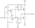
本发明实施例提供一种有机发光显示面板,如图1、图2和图3所示,图1为本发明实施例提供的有机发光显示面板的俯视图一,图2为本发明实施例提供的图1沿BB’方向的截面示意图一,图3为本发明实施例提供的图1沿BB’方向的截面示意图二,该有机发光显示面板包括衬底基板1、多个像素驱动电路2、多个有机发光器件3、第一发射驱动电路4、第二发射驱动电路5、扫描驱动电路6和指纹识别传感器7,其中,An embodiment of the present invention provides an organic light-emitting display panel, as shown in FIG. 1 , FIG. 2 and FIG. 3 , FIG. 1 is a
衬底基板1的一面包括显示区域AA和围绕显示区域AA的周边区域NA,显示区域AA包括常规显示子区域AA1和指纹识别子区域AA2;One side of the
多个像素驱动电路2和多个有机发光器件3设置于显示区域AA内,有机发光器件3与像素驱动电路2一一对应电连接;A plurality of
第一发射驱动电路4设置于周边区域NA内,且与常规显示子区域AA1内的多个像素驱动电路2电连接(图1中黑色圆点表示电连接);The first
第二发射驱动电路5设置于周边区域NA内,且与指纹识别子区域AA2内的多个像素驱动电路2电连接;The second
扫描驱动电路6设置于周边区域NA内,且与显示区域AA内的多个像素驱动电路2电连接;The
指纹识别传感器7设置于有机发光器件3靠近衬底基板1的一侧,且指纹识别传感器7在衬底基板1所在平面的垂直投影,位于指纹识别子区域AA2内。The
常规显示子区域AA1在常规显示过程中和指纹识别过程中均进行常规显示,指纹识别子区域AA2在常规显示过程中进行常规显示,在指纹识别过程中同时进行显示和指纹识别。指纹识别子区域AA2可以位于有机发光显示面板的显示区域AA中的任何位置,本发明实施例会在后续内容中进行举例说明。The normal display sub-area AA1 performs normal display during the normal display process and the fingerprint recognition process, and the fingerprint recognition sub-area AA2 performs normal display during the normal display process, and performs both display and fingerprint recognition during the fingerprint recognition process. The fingerprint identification sub-area AA2 may be located at any position in the display area AA of the organic light-emitting display panel, and the embodiments of the present invention will be illustrated in the following content.
在具有以上所述结构的有机发光显示面板中,通过第一发射驱动电路4对常规显示子区域AA1中的有机发光器件3的亮度进行控制,并通过第二发射驱动电路5对指纹识别子区域AA2中的有机发光器件3的亮度进行控制,进而可以对有机发光显示面板的常规显示子区域AA1的亮度和指纹识别子区域AA2的亮度进行独立控制,在从常规显示过程切换至指纹识别过程时,可以仅通过第二发射驱动电路5控制指纹识别子区域AA2中的有机发光器件3的亮度增大即可,常规显示子区域AA1中的有机发光器件3的亮度不变,进而不会使整个有机发光显示面板的亮度产生突变,有助于使有机发光显示面板具有较好的显示效果。In the organic light-emitting display panel with the above structure, the brightness of the organic light-emitting
在常规显示过程中,常规显示子区域AA1和指纹识别子区域AA2的亮度均较小,以使有机发光显示装置的能耗较低,且不会过分刺激用户的眼睛,即如图4所示,图4为本发明实施例提供的图1在常规显示过程中的工作时序图,在一帧时间内,常规显示子区域AA1和指纹识别子区域AA2内的有机发光器件3不发光的时间较长,具体为:In the conventional display process, the brightness of the conventional display sub-area AA1 and the fingerprint recognition sub-area AA2 are both small, so that the energy consumption of the organic light-emitting display device is low, and the user's eyes are not excessively stimulated, as shown in FIG. 4 . , FIG. 4 is a working timing diagram of FIG. 1 in a conventional display process provided by an embodiment of the present invention. Within one frame, the time when the organic light-emitting
像素驱动电路包括开关晶体管和驱动晶体管,开关晶体管用于控制阳极信号能否到达驱动晶体管的第一端,驱动晶体管用于控制阳极信号经过其到达有机发光器件的电流的大小,开关晶体管由发射信号(第一发射信号和第二发射信号的统称)控制,驱动晶体管由扫描信号控制,以开关晶体管和驱动晶体管均为PMOS晶体管为例,发射信号为高电平时,开关晶体管截止,有机发光器件不发光,发射信号的高电平的持续时间越长,显示区域的亮度越低,因此,在一帧时间内,使第一发射驱动电路4提供的第一发射信号的高电平持续时间较长,第二发射驱动电路5提供的第二发射信号的高电平的持续时间较长,即可使常规显示子区域AA1和指纹识别子区域AA2内的有机发光器件3不发光的时间较长,常规显示子区域AA1和指纹识别子区域AA2的亮度均较小,使有机发光显示装置的能耗较低,且不会过分刺激用户的眼睛。The pixel drive circuit includes a switch transistor and a drive transistor. The switch transistor is used to control whether the anode signal can reach the first end of the drive transistor. The drive transistor is used to control the magnitude of the current through which the anode signal reaches the organic light-emitting device. The switch transistor is driven by the emission signal. (the collective term for the first emission signal and the second emission signal) is controlled, and the driving transistor is controlled by the scanning signal. Taking both the switching transistor and the driving transistor as PMOS transistors as an example, when the emission signal is at a high level, the switching transistor is turned off, and the organic light-emitting device is not When emitting light, the longer the duration of the high level of the emission signal, the lower the brightness of the display area. Therefore, within one frame time, the duration of the high level of the first emission signal provided by the first
图4中,标号Emit1-1指的是,第一发射驱动电路4与常规显示子区域AA1内的第一行像素驱动电路2对应的输出信号,标号Emit2-1指的是,第二发射驱动电路5与指纹识别子区域AA2内的第一行像素驱动电路2对应的输出信号,标号Scan 1指的是,扫描驱动电路6与显示区域AA内的第一行像素驱动电路2对应的输出信号,其他标号的理解方式相同。In FIG. 4, the symbol Emit1-1 refers to the output signal of the first
在指纹识别过程中,常规显示子区域AA1的亮度仍然较小(与常规显示过程中一致),指纹识别子区域AA2的亮度较大,以提高指纹识别传感器7接收到的光线(即有机发光器件3发出的光线经指纹反射后的光线)的强度,使指纹识别更准确,即如图5所示,图5为本发明实施例提供的图1在指纹识别过程中的工作时序图,图5中标号的理解方式与图4相同,此处不再进行赘述,在一帧时间内,常规显示子区域AA1内的有机发光器件3不发光的时间较长,指纹识别子区域AA2内的有机发光器件3不发光的时间较短,具体为:During the fingerprint recognition process, the brightness of the conventional display sub-area AA1 is still small (the same as that in the conventional display process), and the brightness of the fingerprint recognition sub-area AA2 is relatively large, so as to improve the light received by the fingerprint recognition sensor 7 (ie, the organic light-emitting device). 3. The intensity of the light emitted by the light reflected by the fingerprint makes the fingerprint identification more accurate, that is, as shown in FIG. 5, FIG. 5 is the working sequence diagram of FIG. The way of understanding the symbols is the same as that in FIG. 4 , and will not be repeated here. In one frame time, the organic light-emitting
像素驱动电路包括开关晶体管和驱动晶体管,开关晶体管用于控制阳极信号能否到达驱动晶体管的第一端,驱动晶体管用于控制阳极信号经过其到达有机发光器件的电流的大小,开关晶体管由发射信号(第一发射信号和第二发射信号的统称)控制,驱动晶体管由扫描信号控制,以开关晶体管和驱动晶体管均为PMOS晶体管为例,发射信号为高电平时,开关晶体管截止,有机发光器件不发光,发射信号的高电平的持续时间越长,显示区域的亮度越低,因此,在一帧时间内,使第一发射驱动电路4提供的第一发射信号的高电平持续时间较长,第二发射驱动电路5提供的第二发射信号的高电平的持续时间较短,即可使常规显示子区域AA1内的有机发光器件3不发光的时间较长,指纹识别子区域AA2内的有机发光器件3不发光的时间较短,常规显示子区域AA1的亮度较小,指纹识别子区域AA2的亮度较大,以提高指纹识别传感器7接收到的光线的强度,使指纹识别更准确。The pixel drive circuit includes a switch transistor and a drive transistor. The switch transistor is used to control whether the anode signal can reach the first end of the drive transistor. The drive transistor is used to control the magnitude of the current through which the anode signal reaches the organic light-emitting device. The switch transistor is driven by the emission signal. (the collective term for the first emission signal and the second emission signal) is controlled, and the driving transistor is controlled by the scanning signal. Taking both the switching transistor and the driving transistor as PMOS transistors as an example, when the emission signal is at a high level, the switching transistor is turned off, and the organic light-emitting device is not When emitting light, the longer the duration of the high level of the emission signal, the lower the brightness of the display area. Therefore, within one frame time, the duration of the high level of the first emission signal provided by the first
上述“指纹识别传感器7设置于有机发光器件3靠近衬底基板1的一侧”指的是,在有机发光器件3朝向衬底基板1的方向上,设置有指纹识别传感器7,即仅限定了有机发光器件3和指纹识别传感器7的位置关系,并未限定指纹识别传感器7和衬底基板1的位置关系。在一个例子中,如图2所示,指纹识别传感器7设置于有机发光器件3靠近衬底基板1的一侧,且位于有机发光器件3与衬底基板1之间;在又一个例子中,如图3所示,指纹识别传感器7设置于有机发光器件3靠近衬底基板1的一侧,且位于衬底基板1远离有机发光器件3的一侧。The above-mentioned “
可选地,如图2和图3所示,在垂直于衬底基板1的方向上,显示区域AA内,有机发光器件3位于像素驱动电路2远离衬底基板1的一侧,以使得在显示过程中,像素驱动电路2中的不透光结构不会遮挡有机发光器件3发出的光线,使得有机发光显示面板的亮度较高。Optionally, as shown in FIG. 2 and FIG. 3 , in the direction perpendicular to the
为了便于本领域技术人员理解和实施,下面本发明实施例对指纹识别子区域AA2所处位置不同时,第一发射驱动电路4和第二发射驱动电路5的具体实现方式进行举例说明。In order to facilitate understanding and implementation by those skilled in the art, the following embodiments of the present invention illustrate specific implementations of the first
在第一个例子中,如图1所示,多个像素驱动电路2呈n行m列分布,常规显示子区域AA1和指纹识别子区域AA2沿像素驱动电路2的列方向依次设置,常规显示子区域AA1内设置有x行像素驱动电路2,指纹识别子区域AA2内设置有n-x行像素驱动电路2,n和m均为大于1的正整数,x为大于或等于1且小于n的正整数。其中,x的具体取值可以根据像素驱动电路2在其列方向上的尺寸,以及指纹的尺寸进行合理选择,以使得指纹识别子区域AA2的尺寸足够用作指纹识别,且不会过多的占据显示区域AA。In the first example, as shown in FIG. 1 , a plurality of
基于此,第一发射驱动电路4和第二发射驱动电路5的具体实现方式可以如下:Based on this, the specific implementation of the first
如图6所示,图6为本发明实施例提供的第一发射驱动电路的结构示意图一,第一发射驱动电路4包括相互级联的x级第一移位寄存器(图6中表示为Stage 1~Stage x),第1级至第x级第一移位寄存器的输出端分别电连接第1行至第x行像素驱动电路2,进而使得第1级至第x级第一移位寄存器的输出端可依次向第1行至第x行像素驱动电路2输出第一发射信号,以逐行控制常规显示子区域AA1内的有机发光器件2的发光。As shown in FIG. 6 , FIG. 6 is a schematic structural diagram 1 of a first emission driving circuit provided by an embodiment of the present invention. The first
上述“第1级至第x级第一移位寄存器的输出端分别电连接第1行至第x行像素驱动电路2”具体可以通过以下方式实现:如图1所示,有机发光显示面板包括多条第一栅线G1,一条第一栅线G1与一行像素驱动电路2对应电连接,第1级至第x级第一移位寄存器的输出端分别电连接至第1条至第x条第一栅线G1。The above-mentioned "the output terminals of the first shift registers of the first to the xth stage are respectively electrically connected to the
可选地,如图7所示,图7为本发明实施例提供的第一移位寄存器的电路示意图,第一移位寄存器包括第一晶体管M1、第二晶体管M2、第三晶体管M3、第四晶体管M4、第五晶体管M5、第六晶体管M6、第七晶体管M7、第一电容C1、第二电容C2和第三电容C3,其中,Optionally, as shown in FIG. 7 , which is a schematic circuit diagram of a first shift register provided by an embodiment of the present invention, the first shift register includes a first transistor M1, a second transistor M2, a third transistor M3, a Four transistors M4, fifth transistor M5, sixth transistor M6, seventh transistor M7, first capacitor C1, second capacitor C2 and third capacitor C3, wherein,
第一晶体管M1的控制端电连接输入信号端IN,第一晶体管M1的第一端电连接高电平信号端VGH,第一晶体管M1的第二端电连接第四节点N4;第二晶体管M2的控制端电连接第一时钟信号端CK,第二晶体管M2的第一端电连接输入信号端IN,第二晶体管M2的第二端电连接第一节点N1;第三晶体管M3的控制端电连接第四节点N4,第三晶体管M3的第一端电连接低电平信号端VGL,第三晶体管M3的第二端电连接第二节点N2;第四晶体管M4的控制端电连接第一节点N1,第四晶体管M4的第一端电连接高电平信号端VGH,第四晶体管M4的第二端电连接第二节点N2;第五晶体管M5的控制端电连接输出信号端IN,第五晶体管M5的第一端电连接第二时钟信号端XCK,第五晶体管M5的第二端电连接第三节点N3;第六晶体管M6的控制端电连接第二节点N2,第六晶体管M6的第一端电连接高电平信号端VGH,第六晶体管M6的第二端电连接输出端OUT;第七晶体管M7的控制端电连接第一节点N1,第七晶体管M7的第一端电连接低电平信号端VGL,第七晶体管M7的第二端电连接输出端OUT;第一电容C1的第一端电连接第一时钟信号端CK,第一电容C1的第二端电连接第四节点N4;第二电容C2的第一端电连接第一节点N1,第二电容C2的第二端电连接第五节点N5;第三电容C3的第一端电连接高电平信号端CK,第三电容C3的第二端电连接第二节点N2。第一晶体管M1~第七晶体管M7均为PMOS晶体管,其在控制端为低电平时导通,控制端为高电平时截止。The control terminal of the first transistor M1 is electrically connected to the input signal terminal IN, the first terminal of the first transistor M1 is electrically connected to the high-level signal terminal VGH, and the second terminal of the first transistor M1 is electrically connected to the fourth node N4; the second transistor M2 The control terminal of the second transistor M2 is electrically connected to the first clock signal terminal CK, the first terminal of the second transistor M2 is electrically connected to the input signal terminal IN, the second terminal of the second transistor M2 is electrically connected to the first node N1; the control terminal of the third transistor M3 is electrically connected to the first node N1. Connected to the fourth node N4, the first terminal of the third transistor M3 is electrically connected to the low-level signal terminal VGL, the second terminal of the third transistor M3 is electrically connected to the second node N2; the control terminal of the fourth transistor M4 is electrically connected to the first node N1, the first terminal of the fourth transistor M4 is electrically connected to the high-level signal terminal VGH, the second terminal of the fourth transistor M4 is electrically connected to the second node N2; the control terminal of the fifth transistor M5 is electrically connected to the output signal terminal IN, and the fifth transistor M5 is electrically connected to the output signal terminal IN. The first terminal of the transistor M5 is electrically connected to the second clock signal terminal XCK, the second terminal of the fifth transistor M5 is electrically connected to the third node N3; the control terminal of the sixth transistor M6 is electrically connected to the second node N2, and the first terminal of the sixth transistor M6 is electrically connected to the second node N2. One end is electrically connected to the high-level signal end VGH, the second end of the sixth transistor M6 is electrically connected to the output end OUT; the control end of the seventh transistor M7 is electrically connected to the first node N1, and the first end of the seventh transistor M7 is electrically connected to the low The level signal terminal VGL, the second terminal of the seventh transistor M7 is electrically connected to the output terminal OUT; the first terminal of the first capacitor C1 is electrically connected to the first clock signal terminal CK, and the second terminal of the first capacitor C1 is electrically connected to the fourth node N4; the first terminal of the second capacitor C2 is electrically connected to the first node N1, the second terminal of the second capacitor C2 is electrically connected to the fifth node N5; the first terminal of the third capacitor C3 is electrically connected to the high-level signal terminal CK, and the first terminal of the third capacitor C3 is electrically connected to the high-level signal terminal CK. The second terminal of the three capacitors C3 is electrically connected to the second node N2. The first transistor M1 to the seventh transistor M7 are all PMOS transistors, which are turned on when the control terminal is at a low level, and turned off when the control terminal is at a high level.
如图8所示,图8为本发明实施例提供的第一移位寄存器的工作时序图,第一移位寄存器的工作过程包括:As shown in FIG. 8 , FIG. 8 is a working timing diagram of the first shift register provided by an embodiment of the present invention. The working process of the first shift register includes:
第一阶段T1,输入信号端IN提供的输入信号为低电平,第一时钟信号端CK提供的第一时钟信号为低电平,第二时钟信号端XCK提供的第二时钟信号为高电平,由输入信号控制的第一晶体管M1导通,高电平信号端VGH提供的高电平信号经第一晶体管M1到达第四节点N4,第四节点N4为高电平,第三晶体管M3截止,由第一时钟信号控制的第二晶体管M2导通,输入信号经第二晶体管M2到达第一节点N1,第一节点N1为低电平,第四晶体管M4导通,高电平信号端VGH提供的高电平信号经第四晶体管M4到达第二节点N2,第二节点N2为高电平,在第一节点N1的低电平的作用下,第七晶体管M7导通,在第二节点N2的高电平的作用下,第六晶体管M6截止,低电平信号端VGL提供的低电平信号经第七晶体管M7到达输出端OUT,输出端OUT输出低电平,第五晶体管M5导通,第二时钟信号端XCK提供的第二时钟信号到达第三节点N3,第三节点N3为高电平。In the first stage T1, the input signal provided by the input signal terminal IN is low level, the first clock signal provided by the first clock signal terminal CK is low level, and the second clock signal provided by the second clock signal terminal XCK is high level level, the first transistor M1 controlled by the input signal is turned on, the high-level signal provided by the high-level signal terminal VGH reaches the fourth node N4 through the first transistor M1, the fourth node N4 is at a high level, and the third transistor M3 off, the second transistor M2 controlled by the first clock signal is turned on, the input signal reaches the first node N1 through the second transistor M2, the first node N1 is low level, the fourth transistor M4 is turned on, and the high level signal terminal The high-level signal provided by VGH reaches the second node N2 through the fourth transistor M4, and the second node N2 is at a high level. Under the action of the low level of the first node N1, the seventh transistor M7 is turned on. Under the action of the high level of the node N2, the sixth transistor M6 is turned off, the low level signal provided by the low level signal terminal VGL reaches the output terminal OUT through the seventh transistor M7, the output terminal OUT outputs a low level, and the fifth transistor M5 When turned on, the second clock signal provided by the second clock signal terminal XCK reaches the third node N3, and the third node N3 is at a high level.
第二阶段T2,输入信号为高电平,第一时钟信号为高电平,第二时钟信号为低电平,由输入信号控制的第一晶体管M1截止,第四节点N4悬浮,由于第一时钟信号由第一阶段T1的低电平变为高电平,在第一电容C1的耦合作用下第四节点N4的电平更高,第三晶体管M3截止,由第一时钟信号控制的第二晶体管M2截止,第二电容C2放电维持第一节点N1的低电平,第四晶体管M4导通,高电平信号端VGH提供的高电平信号经第四晶体管M4到达第二节点N2,第二节点N2为高电平,在第一节点N1的低电平的作用下,第七晶体管M7导通,在第二节点N2的高电平的作用下,第六晶体管M6截止,低电平信号端VGL提供的低电平信号经第七晶体管M7到达输出端OUT,输出端OUT输出低电平,第五晶体管M5导通,第二时钟信号端XCK提供的第二时钟信号到达第三节点N3,第三节点N3为低电平。In the second stage T2, the input signal is high level, the first clock signal is high level, the second clock signal is low level, the first transistor M1 controlled by the input signal is turned off, and the fourth node N4 is floating. The clock signal changes from the low level of the first stage T1 to the high level. Under the coupling action of the first capacitor C1, the level of the fourth node N4 is higher, the third transistor M3 is turned off, and the third transistor M3 is controlled by the first clock signal. The second transistor M2 is turned off, the second capacitor C2 is discharged to maintain the low level of the first node N1, the fourth transistor M4 is turned on, and the high-level signal provided by the high-level signal terminal VGH reaches the second node N2 through the fourth transistor M4, The second node N2 is at a high level. Under the action of the low level of the first node N1, the seventh transistor M7 is turned on. Under the action of the high level of the second node N2, the sixth transistor M6 is turned off, and the low level is turned on. The low level signal provided by the flat signal terminal VGL reaches the output terminal OUT through the seventh transistor M7, the output terminal OUT outputs a low level, the fifth transistor M5 is turned on, and the second clock signal provided by the second clock signal terminal XCK reaches the third The node N3 and the third node N3 are low level.
第三阶段T3,输入信号为高电平,第一时钟信号为低电平,第二时钟信号为高电平,由输入信号控制的第一晶体管M1截止,第四节点N4悬浮,由于第一时钟信号由第二阶段T2的高电平变为低电平,在第一电容C1的耦合作用下,第四节点N4的电平被拉低,第四节点N4为低电平,第三晶体管M3导通,低电平信号端VGL提供的低电平信号经第三晶体管M3到达第二节点N2,第二节点N2为低电平,由第一时钟信号控制的第二晶体管M2导通,输入信号经第二晶体管M2到达第一节点N1,第一节点N1为高电平,第四晶体管M4截止,在第一节点N1的高电平的作用下,第七晶体管M7截止,在第二节点N2的低电平的作用下,第六晶体管M6导通,高电平信号端VGH提供的高电平信号经第六晶体管M6到达输出端OUT,输出端OUT输出高电平,第五晶体管M5截止,第三节点N3悬浮。In the third stage T3, the input signal is at a high level, the first clock signal is at a low level, the second clock signal is at a high level, the first transistor M1 controlled by the input signal is turned off, and the fourth node N4 is floating. The clock signal changes from the high level of the second stage T2 to the low level. Under the coupling effect of the first capacitor C1, the level of the fourth node N4 is pulled down, the fourth node N4 is low level, and the third transistor M3 is turned on, the low-level signal provided by the low-level signal terminal VGL reaches the second node N2 through the third transistor M3, the second node N2 is at a low level, and the second transistor M2 controlled by the first clock signal is turned on, The input signal reaches the first node N1 through the second transistor M2, the first node N1 is at a high level, the fourth transistor M4 is turned off, and under the action of the high level of the first node N1, the seventh transistor M7 is turned off, and at the second Under the action of the low level of the node N2, the sixth transistor M6 is turned on, the high-level signal provided by the high-level signal terminal VGH reaches the output terminal OUT through the sixth transistor M6, the output terminal OUT outputs a high level, and the fifth transistor M5 is turned off, and the third node N3 is suspended.
第四阶段T4,输入信号为低电平,第一时钟信号为高电平,第二时钟信号为低电平,由输入信号控制的第一晶体管M1导通,高电平信号端VGH提供的高电平信号经第一晶体管M1到达第四节点N4,第四节点N4为高电平,第三晶体管M3截止,由第一时钟信号控制的第二晶体管M2截止,第二电容C2放电维持第一节点N1的高电平,第四晶体管M4截止,在第一节点N1的高电平的作用下,第七晶体管M7截止,第三电容C3放电维持第二节点N2的低电平,在第二节点N2的低电平的作用下,第六晶体管M6导通,高电平信号端VGH提供的高电平信号经第六晶体管M6到达输出端OUT,输出端OUT输出高电平,第五晶体管M5截止,第三节点N3悬浮。In the fourth stage T4, the input signal is at a low level, the first clock signal is at a high level, the second clock signal is at a low level, the first transistor M1 controlled by the input signal is turned on, and the high-level signal terminal VGH provides The high level signal reaches the fourth node N4 through the first transistor M1, the fourth node N4 is high level, the third transistor M3 is turned off, the second transistor M2 controlled by the first clock signal is turned off, and the second capacitor C2 discharges to maintain the A high level of the node N1, the fourth transistor M4 is turned off, under the action of the high level of the first node N1, the seventh transistor M7 is turned off, and the third capacitor C3 discharges to maintain the low level of the second node N2. Under the action of the low level of the two nodes N2, the sixth transistor M6 is turned on, the high-level signal provided by the high-level signal terminal VGH reaches the output terminal OUT through the sixth transistor M6, the output terminal OUT outputs a high level, and the fifth The transistor M5 is turned off, and the third node N3 is suspended.
需要说明的是,本发明实施例中虽未特别说明,但必然高电平信号端VGH在第一阶段T1至第四阶段T4均提供高电平信号,低电平信号端VGL在第一阶段T1至第四阶段T4均提供低电平信号。另外,上述第一时钟信号和第二时钟信号具有相同的频率,且二者的使能电平之间无交叠,非使能电平可以有交叠也可以无交叠,在图4所示的例子中,第一时钟信号和第二时钟信号的使能电平均为低电平,非使能电平均为高电平,第一时钟信号和第二时钟信号的低电平无交叠,高电平也无交叠。It should be noted that, although not specifically described in the embodiment of the present invention, the high-level signal terminal VGH must provide high-level signals in the first stage T1 to the fourth stage T4, and the low-level signal terminal VGL in the first stage. T1 to the fourth stage T4 all provide low-level signals. In addition, the above-mentioned first clock signal and second clock signal have the same frequency, and there is no overlap between the enable levels of the two, and the non-enable levels may or may not overlap, as shown in FIG. 4 . In the example shown, the enable levels of the first clock signal and the second clock signal are both low levels, the disable levels are both high levels, and the low levels of the first clock signal and the second clock signal do not overlap. , the high level does not overlap.
示例性地,如图6所示,第1级第一移位寄存器的输出端电连接第2级第一移位寄存器信号输入端,第2级第一移位寄存器的输出端电连接第3级第一移位寄存器信号输入端,以此类推,以使得上一级第一移位寄存器的输出信号可以直接作为下一级第一移位寄存器的输入信号,进而可以简化第一发射驱动电路4的结构。Exemplarily, as shown in FIG. 6 , the output end of the first shift register of the first stage is electrically connected to the signal input end of the first shift register of the second stage, and the output end of the first shift register of the second stage is electrically connected to the signal input end of the first shift register of the second stage. The signal input terminal of the first shift register of the first stage, and so on, so that the output signal of the first shift register of the previous stage can be directly used as the input signal of the first shift register of the next stage, which can simplify the first
如图9所示,图9为本发明实施例提供的第二发射驱动电路的结构示意图一,第二发射驱动电路5包括相互级联的n-x级第二移位寄存器(图9中表示为Stage 1~Stage n-x),第1级至第n-x级第二移位寄存器的输出端分别电连接第x+1行至第n行像素驱动电路2,进而使得第1级至第n-x级第二移位寄存器的输出端可依次向第x+1行至第n行像素驱动电路2输出第二发射信号,以逐行控制指纹识别子区域AA2内的有机发光器件2的发光。As shown in FIG. 9 , FIG. 9 is a schematic structural diagram 1 of a second emission drive circuit provided by an embodiment of the present invention. The second
上述“第1级至第n-x级第二移位寄存器的输出端分别电连接第x+1行至第n行像素驱动电路2”具体可以通过以下方式实现:如图1所示,有机发光显示面板包括多条第二栅线G2,一条第二栅线G2与一行像素驱动电路2对应电连接,第1级至第n-x级第二移位寄存器的输出端分别电连接至第x+1条至第n条第二栅线G2。The above-mentioned "the output terminals of the second shift registers from the first stage to the n-x stage are respectively electrically connected to the
第二移位寄存器的具体电路结构和工作时序可参见第一移位寄存器,此处不再进行赘述。For the specific circuit structure and working sequence of the second shift register, reference may be made to the first shift register, which will not be repeated here.
在此例子中,可使第二发射驱动电路的第1级第二移位寄存器的输入信号的起始时刻与第x级第一移位寄存器(即最后一级第一移位寄存器)的输出信号的起始时刻相同,进而可以逐行对有机发光显示面板进行驱动,实现显示。In this example, the starting time of the input signal of the second shift register of the first stage of the second emission driving circuit can be set to be the same as the output of the first shift register of the xth stage (ie, the first shift register of the last stage). The starting time of the signal is the same, so that the organic light emitting display panel can be driven row by row to realize display.
可选地,在此例子中,如图1所示,第一发射驱动电路4和第二发射驱动电路5沿像素驱动电路2的列方向依次设置,且在像素驱动电路2的行方向上,第一发射驱动电路4与常规显示子区域AA1相对应,第二发射驱动电路5与指纹识别子区域AA2相对应,以使第一发射驱动电路4与常规显示子区域AA1内的像素驱动电路2连接方便,第二发射驱动电路5与指纹识别子区域AA2内的像素驱动电路2连接方便。Optionally, in this example, as shown in FIG. 1 , the first
可选地,扫描驱动电路6设置于第一发射驱动电路4和第二发射驱动电路5靠近显示区域AA的一侧,以使得在像素驱动电路2的行方向上,扫描驱动电路6可以很好地与所有行的像素驱动电路2对应,有利于简化扫描驱动电路6与像素驱动电路2之间的连接方式。Optionally, the
在第二个例子中,如图10所示,图10为本发明实施例提供的有机发光显示面板的俯视图二,多个像素驱动电路2呈n行m列分布,常规显示子区域AA1至少部分包围指纹识别子区域AA2,第x1行至第x2行中第y1列至第y2列像素驱动电路2位于指纹识别子区域AA2内,n和m均为大于1的正整数,x1为大于或等于1且小于n的正整数,x2为大于x1且小于或等于n的正整数,y1为大于或等于1且小于m的正整数,y2为大于y1且小于或等于m的正整数。其中,x1、x2、y1和y2的具体取值,可以根据像素驱动电路2在其行方向和列方向上的尺寸,以及指纹的尺寸进行合理选择,以使得指纹识别子区域AA2的尺寸足够用作指纹识别,且不会过多的占据显示区域AA。In the second example, as shown in FIG. 10 , which is a second top view of the organic light emitting display panel provided by the embodiment of the present invention, a plurality of
基于此,第一发射驱动电路4和第二发射驱动电路5的具体实现方式可以如下:Based on this, the specific implementation of the first
如图11所示,图11为本发明实施例提供的第一发射驱动电路的结构示意图二,第一发射驱动电路4包括相互级联的n级第一移位寄存器(图11中表示为Stage 1~Stage n),第1级至第x1-1级第一移位寄存器的输出端分别电连接第1行至第x1-1行像素驱动电路2,第x2+1级至第n级第一移位寄存器的输出端分别电连接第x2+1行至第n行像素驱动电路2,第x1级至第x2级第一移位寄存器的输出端分别电连接第x1行至第x2行中第1列至第y1-1列以及第y2+1列至第m列像素驱动电路2,进而使得第1级至第x1-1级第一移位寄存器的输出端可依次向第1行至第x1-1行像素驱动电路2输出第一发射信号,第x1级至第x2级第一移位寄存器的输出端可依次向第x1行至第x2行中第1列至第y1-1列以及第y2+1列至第m列像素驱动电路2输出第一发射信号,第x2+1级至第n级第一移位寄存器的输出端可依次向第x2+1行至第n行像素驱动电路2输出第一发射信号,以逐行控制常规显示子区域AA1内的有机发光器件2的发光。As shown in FIG. 11 , FIG. 11 is a second structural schematic diagram of a first emission driving circuit provided by an embodiment of the present invention. The first
上述“第1级至第x1-1级第一移位寄存器的输出端分别电连接第1行至第x1-1行像素驱动电路2,第x2+1级至第n级第一移位寄存器的输出端分别电连接第x2+1行至第n行像素驱动电路2,第x1级至第x2级第一移位寄存器的输出端分别电连接第x1行至第x2行中第1列至第y1-1列以及第y2+1列至第m列像素驱动电路2”具体可以通过以下方式实现:如图10所示,有机发光显示面板包括多条第一栅线G1,第1行至第x1-1行像素驱动电路2各与一条第一栅线G1对应电连接,第x2+1行至第n行像素驱动电路2各与一条第一栅线G1对应电连接,第x1行至第x2行中第y1-1列以及第y2+1列像素驱动电路2各与一条第一栅线G1对应电连接,第1级至第n级第一移位寄存器的输出端分别电连接至第1条至第n条第一栅线G1。The outputs of the above-mentioned " 1st to x1-1st stage first shift registers are respectively electrically connected to the
如图12所示,图12为本发明实施例提供的第二发射驱动电路的结构示意图二,第二发射驱动电路5包括相互级联的x2-x1+1级第二移位寄存器,第1级至第x2-x1+1级第二移位寄存器的输出端分别电连接第x1行至第x2行中第y1列至第y2列像素驱动电路2,进而使得第1级至第x2-x1+1级第二移位寄存器的输出端可依次向第x1行至第x2行中第y1列至第y2列像素驱动电路2输出第二发射信号,以逐行控制指纹识别子区域AA2内的有机发光器件2的发光。As shown in FIG. 12 , FIG. 12 is a second structural schematic diagram of a second emission driving circuit provided by an embodiment of the present invention. The second
上述“第1级至第x2-x1+1级第二移位寄存器的输出端分别电连接第x1行至第x2行中第y1列至第y2列像素驱动电路2”具体可以通过以下方式实现:如图10所示,有机发光显示面板包括多条第二栅线G2,第x1行至第x2行中第y1列至第y2列像素驱动电路2各与一条第二栅线G2对应电连接,第1级至第x2-x1+1级第二移位寄存器的输出端分别电连接至第1条至第x2-x1+1条第二栅线G2。The above-mentioned "the output terminals of the second shift registers of the first to x 2 -x 1 +1 stages are respectively electrically connected to the
在此例子中,第一移位寄存器和第二移位寄存器的具体电路结构和工作时序均可参见第一移位寄存器,此处不再进行赘述。In this example, the specific circuit structures and working timings of the first shift register and the second shift register can refer to the first shift register, which will not be repeated here.
在此例子中,可使第二发射驱动电路的第1级第二移位寄存器的输入信号的起始时刻与第x1级第一移位寄存器的输出信号的起始时刻相同,进而可以使得第x1级第一移位寄存器对第x1行像素驱动电路的驱动,与第1级第二移位寄存器对第x1+1行像素驱动电路的驱动之间只间隔一行的扫描时间,与其他行之间间隔的扫描时间相同,进而可以逐行对有机发光显示面板进行驱动,实现显示,第一发射驱动电路和第二发射驱动电路的设置未对有机发光显示面板的显示效果产生不良影响。In this example, the start time of the input signal of the first-stage second shift register of the second emission driving circuit can be made the same as the start time of the output signal of the x1 - stage first shift register, so as to make There is only one scan time interval between the driving of the pixel driving circuit of the x1th row by the first shift register of the x1st stage and the driving of the pixel driving circuit of the x1 + 1th row by the second shift register of the first stage. The scanning time is the same as the interval between other rows, so that the organic light emitting display panel can be driven row by row to realize display, and the settings of the first emission driving circuit and the second emission driving circuit do not have any adverse effects on the display effect of the organic light emitting display panel. influences.
可选地,在此例子中,如图10所示,第一发射驱动电路4沿像素驱动电路2的列方向设置,第二发射驱动电路5位于第一发射驱动电路4靠近显示区域AA的一侧或者远离显示区域AA的一侧(图10中仅以第二发射驱动电路5位于第一发射驱动电路4靠近显示区域AA的一侧为例),且在像素驱动电路2的行方向上,第二发射驱动电路5与指纹识别子区域AA2相对应,以使第一发射驱动电路4与常规显示子区域AA1内的像素驱动电路2连接方便,第二发射驱动电路5与指纹识别子区域AA2内的像素驱动电路2连接方便。Optionally, in this example, as shown in FIG. 10 , the first
可选地,如图10所示,扫描驱动电路(图10中未示出)设置于第一发射驱动电路4和第二发射驱动电路5靠近显示区域AA的一侧,以使得在像素驱动电路2的行方向上,扫描驱动电路可以很好地与所有行的像素驱动电路2对应,有利于简化扫描驱动电路与像素驱动电路2之间的连接方式。Optionally, as shown in FIG. 10 , a scan driving circuit (not shown in FIG. 10 ) is disposed on one side of the first
可选地,如图13所示,图13为本发明实施例提供的像素驱动电路的电路示意图,本发明实施例中像素驱动电路2包括第八晶体管M8、第九晶体管M9、驱动晶体管Td和第四电容C4,其中,第八晶体管M8的控制端电连接扫描信号输入端Scan,第八晶体管M8的第一端电连接显示信号输入端Vdata,第八晶体管M8的第二端电连接驱动晶体管Td的控制端;驱动晶体管Td的控制端电连接第八晶体管M8的第二端,驱动晶体管Td的第一端电连接第九晶体管M9的第二端,驱动晶体管Td的第二端电连接有机发光器件3的阳极;第九晶体管M9的控制端电连接发射信号输入端Emit,第九晶体管M9的第一端电连接阳极信号输入端PVDD,第九晶体管M9的第二端电连接驱动晶体管Td的第一端;第四电容C4的第一端电连接驱动晶体管Td的控制端,第四电容C4的第二端电连接阳极信号输入端PVDD。第八晶体管M8、第九晶体管M9和驱动晶体管Td均为PMOS晶体管。Optionally, as shown in FIG. 13, FIG. 13 is a schematic circuit diagram of a pixel driving circuit provided by an embodiment of the present invention. In this embodiment of the present invention, the pixel driving circuit 2 includes an eighth transistor M8, a ninth transistor M9, a driving transistor Td and The fourth capacitor C4, wherein the control terminal of the eighth transistor M8 is electrically connected to the scan signal input terminal Scan, the first terminal of the eighth transistor M8 is electrically connected to the display signal input terminal Vdata, and the second terminal of the eighth transistor M8 is electrically connected to the driving transistor The control terminal of Td; the control terminal of the driving transistor Td is electrically connected to the second terminal of the eighth transistor M8, the first terminal of the driving transistor Td is electrically connected to the second terminal of the ninth transistor M9, and the second terminal of the driving transistor Td is electrically connected to the organic The anode of the light-emitting device 3; the control terminal of the ninth transistor M9 is electrically connected to the emission signal input terminal Emit, the first terminal of the ninth transistor M9 is electrically connected to the anode signal input terminal PVDD, and the second terminal of the ninth transistor M9 is electrically connected to the driving transistor Td The first terminal of the fourth capacitor C4 is electrically connected to the control terminal of the driving transistor Td, and the second terminal of the fourth capacitor C4 is electrically connected to the anode signal input terminal PVDD. The eighth transistor M8, the ninth transistor M9 and the driving transistor Td are all PMOS transistors.
其中,在显示过程(包括常规显示过程和指纹识别过程)中,驱动晶体管Td的控制端之间的电压与其第一端之间的电压之间的差值小于其阈值电压时,驱动晶体管Td处于截止状态,该差值大于或等于其阈值电压时,驱动晶体管Td处于导通状态,且该差值越大驱动晶体管Td导通越完全,经过驱动晶体管Td的电流越大,进而使得有机发光器件3的发光电流越大,亮度越大。Wherein, in the display process (including the conventional display process and the fingerprint identification process), when the difference between the voltage between the control terminals of the driving transistor Td and the voltage between the first terminals thereof is less than its threshold voltage, the driving transistor Td is in the In the off state, when the difference is greater than or equal to its threshold voltage, the driving transistor Td is in an on state, and the greater the difference, the more complete the conduction of the driving transistor Td, the greater the current passing through the driving transistor Td, thereby making the organic light-emitting device The greater the luminous current of 3, the greater the brightness.
如图14所示,图14为本发明实施例提供的像素驱动电路的工作时序图,像素驱动电路2驱动有机发光器件3的过程包括:As shown in FIG. 14, FIG. 14 is a working timing diagram of a pixel driving circuit provided by an embodiment of the present invention. The process of driving the organic light-emitting
在第一阶段T1,扫描信号输入端Scan提供的扫描信号为低电平,发射信号输入端Emit提供的发射信号为高电平,由扫描信号控制的第八晶体管M8导通,由发射信号控制的第九晶体管M9截止,显示信号输入端Vdata提供的显示信号经第八晶体管M8到达驱动晶体管Td的控制端,且为第四电容C4充电,驱动晶体管Td导通,有机发光器件3不发光;In the first stage T1, the scan signal provided by the scan signal input terminal Scan is at a low level, the transmit signal provided by the transmit signal input terminal Emit is at a high level, and the eighth transistor M8 controlled by the scan signal is turned on and controlled by the transmit signal The ninth transistor M9 is turned off, the display signal provided by the display signal input terminal Vdata reaches the control terminal of the driving transistor Td through the eighth transistor M8, and charges the fourth capacitor C4, the driving transistor Td is turned on, and the organic light-emitting
在第二阶段T2,扫描信号输入端Scan提供的扫描信号为高电平,发射信号输入端Emit提供的发射信号为低电平,由扫描信号控制的第八晶体管M8截止,由发射信号控制的第九晶体管M9导通,第四电容C4放电维持驱动晶体管Td导通,发光电流经过第九晶体管M9和驱动晶体管Td,进而流经有机发光器件3,驱动有机发光器件3发光。In the second stage T2, the scan signal provided by the scan signal input terminal Scan is high level, the transmit signal provided by the transmit signal input terminal Emit is low level, the eighth transistor M8 controlled by the scan signal is turned off, and the transistor M8 controlled by the transmit signal is turned off. The ninth transistor M9 is turned on, the fourth capacitor C4 discharges to keep the driving transistor Td turned on, the light-emitting current flows through the ninth transistor M9 and the driving transistor Td, and then flows through the organic light-emitting
此外,本发明实施例中,多个有机发光器件3包括用于发射红光的有机发光器件3、用于发射绿光的有机发光器件3和用于发射蓝光的有机发光器件3,以使有机发光显示面板可实现全彩显示。In addition, in the embodiment of the present invention, the plurality of organic light-emitting
进一步地,发明人发现,有机发光显示面板中,用于发射红光的有机发光器件3以及用于发射绿光的有机发光器件3的发光强度均较高,用于发射蓝光的有机发光器件3的发光强度较低,因此,在本发明实施例中,指纹识别传感器7用于接收指纹反射的多个有机发光器件3发射的红光进行指纹识别,或者,接收指纹反射的多个有机发光器件3发射的绿光进行指纹识别,或者,接收指纹反射的多个有机发光器件3发射的光线混合而成的白光进行指纹识别,以使得一方面无需为指纹识别传感器7额外设置光源,有助于简化有机发光显示面板的结构,另一方面,保证指纹识别的准确性。Further, the inventor found that in the organic light-emitting display panel, the organic light-emitting
可选地,本发明实施例中有机发光器件3为有机发光二极管,以使有机发光器件3具有自发光、高亮度、广视角、快速反应等优良特性。Optionally, in the embodiment of the present invention, the organic light-emitting
进一步地,如图15所示,图15为本发明实施例提供的有机发光器件的截面示意图,有机发光器件3包括沿远离衬底基板1方向依次层叠设置的阳极31、有机发光功能层32和阴极33,有机发光功能层32包括沿远离衬底基板1方向依次层叠设置的空穴注入层32a、空穴传输层32b、发光层32c、电子传输层32d和电子注入层32e。可选地,所有有机发光二极管的阴极33为一整层结构,以使得有机发光显示面板的结构简单,驱动方便。Further, as shown in FIG. 15 , which is a schematic cross-sectional view of an organic light-emitting device according to an embodiment of the present invention, the organic light-emitting
具体地,有机发光器件3工作过程中,阴极33产生电子,阳极31产生空穴,在阴极33和阳极31之间的电场作用下,空穴经过空穴注入层32a和空穴传输层32b向发光层32c移动,电子经过电子注入层32e和电子传输层32d向发光层32c移动,当空穴和电子在发光层32c中相遇后,二者复合释放能量,从而使该有机发光器件3发出光线。Specifically, during the operation of the organic light-emitting
此外,本发明实施例还提供一种有机发光显示装置,如图16所示,图16为本发明实施例提供的有机发光显示装置的结构示意图,有机发光显示装置包括以上任一项所述的有机发光显示面板600。In addition, an embodiment of the present invention also provides an organic light-emitting display device, as shown in FIG. 16 , which is a schematic structural diagram of the organic light-emitting display device provided by the embodiment of the present invention. The organic light-emitting display device includes any of the above The organic light emitting
本发明实施例提供的有机发光显示装置可以是例如智能手机、可穿戴式智能手表、智能眼镜、平板电脑、电视机、显示器、笔记本电脑、数码相框、导航仪、车载显示器、电子书等任何具有显示功能的产品或部件。本申请实施例提供的显示面板和显示装置可以为柔性,也可以为非柔性,本申请对此不做限定。The organic light-emitting display device provided by the embodiment of the present invention may be, for example, a smart phone, a wearable smart watch, smart glasses, a tablet computer, a TV, a monitor, a notebook computer, a digital photo frame, a navigator, a car display, an e-book, etc. A product or part that displays functionality. The display panel and the display device provided in the embodiments of the present application may be flexible or non-flexible, which is not limited in the present application.
此外,本发明实施例还提供一种有机发光显示面板的驱动方法,适用于以上任一项所述的有机发光显示面板,如图17所示,图17为本发明实施例提供的有机发光显示面板的驱动方法的流程图,该有机发光显示面板的驱动方法包括:In addition, an embodiment of the present invention also provides a driving method for an organic light-emitting display panel, which is applicable to the organic light-emitting display panel described in any of the above. As shown in FIG. 17 , FIG. 17 is the organic light-emitting display panel provided by the embodiment of the present invention. A flowchart of a method for driving a panel, the method for driving an organic light-emitting display panel includes:
将有机发光显示面板的各帧划分为常规显示帧和指纹识别帧,其中,Each frame of the organic light emitting display panel is divided into a regular display frame and a fingerprint identification frame, wherein,
在常规显示帧:扫描驱动电路6为显示区域AA内的像素驱动电路2提供扫描信号,第一发射驱动电路4为常规显示子区域AA1内的各像素驱动电路2提供第一发射信号,第二发射驱动电路5为指纹识别子区域AA2内的各像素驱动电路2提供第二发射信号,第一发射信号的高电平(即使能电平)出现次数和各次持续时间,与第二发射信号的高电平(即使能电平)出现次数和各次持续时间均相同;In a normal display frame: the
在指纹识别帧:扫描驱动电路6为显示区域AA内的像素驱动电路2提供扫描信号,第一发射驱动电路4为常规显示子区域AA1内的各像素驱动电路2提供第一发射信号,第二发射驱动电路5为指纹识别子区域AA2内的各像素驱动电路2提供第三发射信号,指纹识别传感器7接收指纹反射的光线进行指纹识别,第三发射信号的高电平(即使能电平)出现次数低于第一发射信号的高电平(即使能电平)出现次数,和/或,第三发射信号的高电平(即使能电平)的各次持续时间,短于第一发射信号的高电平(即使能电平)的各次持续时间。In the fingerprint identification frame: the
之前所述的指纹识别过程包括至少一个指纹识别帧,常规显示过程包括至少一个常规显示帧。The fingerprinting process described earlier includes at least one fingerprinting frame, and the regular display process includes at least one regular display frame.
在常规显示帧中,由于第一发射信号的高电平(即使能电平)出现次数和各次持续时间,与第二发射信号的高电平(即使能电平)出现次数和各次持续时间均相同,从而使得常规显示子区域AA1的亮度和指纹识别子区域AA2的亮度相同,有机发光显示面板的亮度一致,显示效果较好。In a conventional display frame, due to the number of occurrences and durations of high levels (ie, enable levels) of the first transmit signal, the number of occurrences and durations of high levels (ie, enable levels) of the second transmit signal The time is the same, so that the brightness of the conventional display sub-area AA1 and the brightness of the fingerprint identification sub-area AA2 are the same, the brightness of the organic light-emitting display panel is the same, and the display effect is better.
在指纹识别帧,由于第三发射信号的高电平(即使能电平)出现次数低于第一发射信号的高电平(即使能电平)出现次数,和/或,第三发射信号的高电平(即使能电平)的各次持续时间,短于第一发射信号的高电平(即使能电平)的各次持续时间,从而使得常规显示子区域AA1的亮度与常规显示帧相同,而指纹识别子区域AA2的亮度大于常规显示帧,使得指纹识别的准确性好。In the fingerprint identification frame, since the number of occurrences of the high level (ie the enable level) of the third transmit signal is lower than the number of occurrences of the high level (ie the enable level) of the first transmit signal, and/or, the number of occurrences of the third transmit signal The duration of each time of the high level (ie, the enable level) is shorter than the duration of each time of the high level (ie, the enable level) of the first transmit signal, so that the brightness of the regular display sub-area AA1 is the same as that of the regular display frame. The same, but the brightness of the fingerprint identification sub-area AA2 is larger than that of the conventional display frame, so that the accuracy of fingerprint identification is good.
在满足上述第一发射信号、第二发射信号和第三发射信号之间的关系时,第一发射信号、第二发射信号和第三发射信号的具体设置方式可以有多种,下面本发明实施例进行举例说明。When the above-mentioned relationship between the first transmission signal, the second transmission signal and the third transmission signal is satisfied, the specific setting methods of the first transmission signal, the second transmission signal and the third transmission signal can be various, and the present invention is implemented below. Example to illustrate.
在一个例子中,在常规显示帧:第一发射信号和第二发射信号的高电平出现次数均为p1次(例如3次),各次持续时间均为T1(例如两个时间段);在指纹识别帧:第一发射信号的高电平出现次数为p1次,各次持续时间均为T1,第三发射信号的高电平出现次数为p2次(例如1次),持续时间均为T1;其中,p1和p2均为正整数,且p1大于p2。In an example, in a conventional display frame: the number of high-level occurrences of the first transmit signal and the second transmit signal is p1 times (for example, 3 times), and the duration of each time is T1 ( for example, two time periods) ; In the fingerprint identification frame: the number of high-level occurrences of the first transmission signal is p1 times, and the duration of each time is T 1 , and the number of high-level occurrences of the third transmission signal is p2 times (for example, 1 time), and the duration Both are T 1 ; wherein, p1 and p2 are both positive integers, and p1 is greater than p2.
在有一个例子中,在常规显示帧:第一发射信号和第二发射信号的高电平出现次数均为q次(例如1次),持续时间均为T2;在指纹识别帧:第一发射信号的高电平出现次数为q次,持续时间为T2,第三发射信号的高电平出现次数为q次,持续时间为T3,T3小于T2;其中,q为正整数。可选地,T3为T2/3。In one example, in a conventional display frame: the high-level occurrences of the first transmit signal and the second transmit signal are both q times (for example, 1 time), and the durations are both T 2 ; in the fingerprint identification frame: the first The number of high-level occurrences of the transmit signal is q times, and the duration is T 2 , the number of high-level occurrences of the third transmit signal is q times, the duration is T 3 , and T 3 is less than T 2 ; wherein, q is a positive integer . Optionally, T 3 is T 2 /3.
另外,扫描驱动电路6提供的扫描信号的个数可以为一个或多个(例如两个),为了较好地驱动像素驱动电路2进而驱动有机发光器件3发光,本发明实施例中选择第一发射信号、第二发射信号和第三发射信号的高电平的各次持续时间均大于或等于扫描驱动电路6提供的各扫描信号的低电平的持续时间之和,以使得在有机发光器件3发光之前,可以有足够的时间在其连接的驱动晶体管的控制端上写入信号,使得有机发光器件3的发光效果较好。例如,第一发射信号、第二发射信号和第三发射信号的高电平的各次持续时间均为两个阶段,扫描驱动电路6提供两个扫描信号,两个扫描信号的低电平的持续时间各为一个阶段。In addition, the number of scan signals provided by the
可选地,本发明实施例中,多个有机发光器件3包括用于发射红光的有机发光器件3、用于发射绿光的有机发光器件3和用于发射蓝光的有机发光器件3,以使有机发光显示面板可实现全彩显示。Optionally, in the embodiment of the present invention, the plurality of organic light-emitting
进一步地,本发明实施例中选择,在指纹识别帧:指纹识别传感器7接收指纹反射的红光进行指纹识别;或者,指纹识别传感器7接收指纹反射的绿光进行指纹识别;或者,指纹识别传感器7接收指纹反射的白光进行指纹识别,以使得一方面无需为指纹识别传感器7额外设置光源,有助于简化有机发光显示面板的结构,另一方面,保证指纹识别的准确性。Further, in the embodiment of the present invention, in the fingerprint identification frame: the
可选地,如图1、图6和图9所示,多个像素驱动电路2呈n行m列分布,常规显示子区域AA1和指纹识别子区域AA2沿像素驱动电路2的列方向依次设置,常规显示子区域AA1内设置有x行像素驱动电路2,指纹识别子区域AA2内设置有n-x行像素驱动电路2,n和m均为大于1的正整数,x为大于或等于1且小于n的正整数;第一发射驱动电路4包括相互级联的x级第一移位寄存器,第1级至第x级第一移位寄存器的输出端分别电连接第1行至第x行像素驱动电路2;第二发射驱动电路5包括相互级联的n-x级第二移位寄存器,第1级至第n-x级第二移位寄存器的输出端分别电连接第x+1行至第n行像素驱动电路2。Optionally, as shown in FIG. 1 , FIG. 6 and FIG. 9 , a plurality of
基于此,本发明实施例中选择,在常规显示帧:第1级第二移位寄存器的输入信号与第x级第一移位寄存器的输出的第一发射信号相同,以使指纹识别子区域AA2的亮度与常规显示子区域AA1的亮度相同;在指纹识别帧:第1级第二移位寄存器的输入信号的高电平,与第x级第一移位寄存器的输出的第一发射信号的高电平开始时刻相同,第1级第二移位寄存器的输入信号的高电平的持续时间,短于第x级第一移位寄存器的输出的第一发射信号的高电平的持续时间,以使指纹识别子区域AA2的亮度大于常规显示子区域AA1的亮度。Based on this, in the embodiment of the present invention, in the conventional display frame: the input signal of the second shift register of the first stage is the same as the first transmission signal of the output of the first shift register of the xth stage, so that the fingerprint identification sub-area The brightness of AA2 is the same as the brightness of the conventional display sub-area AA1; in the fingerprint identification frame: the high level of the input signal of the second shift register of the first stage, and the output of the first transmission signal of the first shift register of the xth stage The high-level start time is the same, and the high-level duration of the input signal of the first-stage second shift register is shorter than the high-level duration of the output signal of the xth-stage first shift register. time, so that the brightness of the fingerprint identification sub-area AA2 is greater than that of the conventional display sub-area AA1.
可选地,如图10、图11和图12所示,多个像素驱动电路2呈n行m列分布,常规显示子区域AA1至少部分包围指纹识别子区域AA2,第x1行至第x2行中第y1列至第y2列像素驱动电路2位于指纹识别子区域AA2内,n和m均为大于1的正整数,x1为大于或等于1且小于n的正整数,x2为大于x1且小于或等于n的正整数,y1为大于或等于1且小于m的正整数,y2为大于y1且小于或等于m的正整数;第一发射驱动电路4包括相互级联的n级第一移位寄存器,第1级至第x1-1级第一移位寄存器的输出端分别电连接第1行至第x1-1行像素驱动电路2,第x2+1级至第n级第一移位寄存器的输出端分别电连接第x2+1行至第n行像素驱动电路2,第x1级至第x2级第一移位寄存器的输出端分别电连接第x1行至第x2行中第1列至第y1-1列以及第y2+1列至第m列像素驱动电路2;第二发射驱动电路5包括相互级联的x2-x1+1级第二移位寄存器,第1级至第x2-x1+1级第二移位寄存器的输出端分别电连接第x1行至第x2行中第y1列至第y2列像素驱动电路2;Optionally, as shown in FIG. 10 , FIG. 11 and FIG. 12 , the plurality of pixel driving circuits 2 are distributed in n rows and m columns, the conventional display sub-area AA1 at least partially surrounds the fingerprint identification sub-area AA2, and the x 1th row to the xth In the 2nd row, the pixel drive circuit 2 of the y1th column to the y2th column is located in the fingerprint identification sub-area AA2, n and m are both positive integers greater than 1, x 1 is a positive integer greater than or equal to 1 and less than n, x 2 is a positive integer greater than x 1 and less than or equal to n, y 1 is a positive integer greater than or equal to 1 and less than m, y 2 is a positive integer greater than y 1 and less than or equal to m; the first emission drive circuit 4 includes The n -stage first shift registers are cascaded with each other, and the outputs of the first to x1-1 first shift registers are electrically connected to the pixel drive circuits 2 from the first row to the x1-1 row respectively, and the x The outputs of the first shift registers from the 2 +1st stage to the nth stage are respectively electrically connected to the pixel driving circuits 2 from the x2 + 1th row to the nth row, and the outputs of the first shift registers from the x1st stage to the x2th stage are respectively connected. The terminals are respectively electrically connected to the
基于此,本发明实施例中选择,在常规显示帧:第1级第二移位寄存器的输入信号与第x1-1级第一移位寄存器的输出的第一发射信号相同,以使指纹识别子区域AA2的亮度与常规显示子区域AA1的亮度相同;在指纹识别帧:第1级第二移位寄存器的输入信号的高电平,与第x1-1级第一移位寄存器的输出的第一发射信号的高电平开始时刻相同,第1级第二移位寄存器的输入信号的高电平的持续时间,短于第x1-1级第一移位寄存器的输出的第一发射信号的高电平的持续时间,以使指纹识别子区域AA2的亮度大于常规显示子区域AA1的亮度。其相关原理可以参见之前关于图4和图5的相关描述,此处不再进行赘述。Based on this, in the embodiment of the present invention, in the conventional display frame: the input signal of the second shift register of the 1st stage is the same as the first transmission signal of the output of the first shift register of the x1-1st stage, so that the fingerprint The brightness of the identification sub-area AA2 is the same as that of the conventional display sub-area AA1; in the fingerprint identification frame: the high level of the input signal of the second shift register of the first stage is the same as that of the first shift register of the x 1 -1 stage. The high-level start time of the output first transmit signal is the same, and the high-level duration of the input signal of the first stage of the second shift register is shorter than the output of the x 1 -1 stage of the first shift register. The duration of a high level of the transmission signal, so that the brightness of the fingerprint identification sub-area AA2 is greater than that of the conventional display sub-area AA1. For the related principles, reference may be made to the previous related descriptions about FIG. 4 and FIG. 5 , which will not be repeated here.
需要说明的是,本发明实施例中的有机发光显示面板的相关内容均适用于其驱动方法,同样地,有机发光显示面板的驱动方法的相关内容也均适用于有机发光显示面板,文中不再进行赘述。It should be noted that the relevant content of the organic light emitting display panel in the embodiments of the present invention is applicable to the driving method thereof. Similarly, the relevant content of the driving method of the organic light emitting display panel is also applicable to the organic light emitting display panel. Repeat.
本发明实施例提供了一种有机发光显示面板及其驱动方法、有机发光显示装置,该有机发光显示面板包括第一发射驱动电路4和第二发射驱动电路5,其中,第一发射驱动电路4设置于周边区域NA内,且与常规显示子区域AA1内的多个像素驱动电路2电连接,第二发射驱动电路5设置于周边区域NA内,且与指纹识别子区域AA2内的多个像素驱动电路2电连接,通过第一发射驱动电路4对常规显示子区域AA1中的有机发光器件3的亮度进行控制,并通过第二发射驱动电路5对指纹识别子区域AA2中的有机发光器件3的亮度进行控制,进而可以对有机发光显示面板的常规显示子区域AA1的亮度和指纹识别子区域AA2的亮度进行独立控制,在从常规显示过程切换至指纹识别过程时,可以仅通过第二发射驱动电路5控制指纹识别子区域AA2中的有机发光器件3的亮度增大即可,常规显示子区域AA1中的有机发光器件3的亮度不变,进而不会使整个有机发光显示面板的亮度产生突变,有助于使有机发光显示面板具有较好的显示效果。Embodiments of the present invention provide an organic light-emitting display panel, a driving method thereof, and an organic light-emitting display device. The organic light-emitting display panel includes a first
最后应说明的是:以上各实施例仅用以说明本发明的技术方案,而非对其限制;尽管参照前述各实施例对本发明进行了详细的说明,本领域的普通技术人员应当理解:其依然可以对前述各实施例所记载的技术方案进行修改,或者对其中部分或者全部技术特征进行等同替换;而这些修改或者替换,并不使相应技术方案的本质脱离本发明各实施例技术方案的范围。Finally, it should be noted that the above embodiments are only used to illustrate the technical solutions of the present invention, but not to limit them; although the present invention has been described in detail with reference to the foregoing embodiments, those of ordinary skill in the art should understand that: The technical solutions described in the foregoing embodiments can still be modified, or some or all of the technical features thereof can be equivalently replaced; and these modifications or replacements do not make the essence of the corresponding technical solutions deviate from the technical solutions of the embodiments of the present invention. scope.
Claims (20)
Priority Applications (2)
| Application Number | Priority Date | Filing Date | Title |
|---|---|---|---|
| CN201810697105.5A CN108806603B (en) | 2018-06-29 | 2018-06-29 | Organic light-emitting display panel, driving method thereof and organic light-emitting display device |
| US16/181,520 US10672334B2 (en) | 2018-06-29 | 2018-11-06 | Organic light-emitting display panel, method for driving the same, and organic light-emitting display device |
Applications Claiming Priority (1)
| Application Number | Priority Date | Filing Date | Title |
|---|---|---|---|
| CN201810697105.5A CN108806603B (en) | 2018-06-29 | 2018-06-29 | Organic light-emitting display panel, driving method thereof and organic light-emitting display device |
Publications (2)
| Publication Number | Publication Date |
|---|---|
| CN108806603A CN108806603A (en) | 2018-11-13 |
| CN108806603B true CN108806603B (en) | 2020-03-17 |
Family
ID=64073173
Family Applications (1)
| Application Number | Title | Priority Date | Filing Date |
|---|---|---|---|
| CN201810697105.5A Active CN108806603B (en) | 2018-06-29 | 2018-06-29 | Organic light-emitting display panel, driving method thereof and organic light-emitting display device |
Country Status (2)
| Country | Link |
|---|---|
| US (1) | US10672334B2 (en) |
| CN (1) | CN108806603B (en) |
Families Citing this family (22)
| Publication number | Priority date | Publication date | Assignee | Title |
|---|---|---|---|---|
| KR102669730B1 (en) * | 2018-08-02 | 2024-05-28 | 삼성디스플레이 주식회사 | Display device |
| CN109192140B (en) * | 2018-09-27 | 2020-11-24 | 武汉华星光电半导体显示技术有限公司 | Pixel driving circuit and display device |
| CN109545132A (en) * | 2018-11-26 | 2019-03-29 | 昆山国显光电有限公司 | Shield body display methods, display screen and electronic equipment |
| CN109767713A (en) * | 2019-01-09 | 2019-05-17 | 昆山国显光电有限公司 | Display screen, display panel drive method and display device |
| CN109637376B (en) * | 2019-01-31 | 2022-02-18 | 厦门天马微电子有限公司 | Display device |
| CN109801605B (en) * | 2019-02-27 | 2021-01-08 | 维沃移动通信有限公司 | Screen brightness adjusting method, electronic equipment, mobile terminal and storage medium |
| WO2020186481A1 (en) * | 2019-03-20 | 2020-09-24 | 深圳市汇顶科技股份有限公司 | Fingerprint collection method and system, and electronic device |
| CN110310597A (en) * | 2019-06-27 | 2019-10-08 | 云谷(固安)科技有限公司 | A kind of display equipment and display methods |
| CN110428736B (en) * | 2019-07-29 | 2021-04-30 | 厦门天马微电子有限公司 | Display device |
| CN110599905A (en) * | 2019-08-29 | 2019-12-20 | 维沃移动通信有限公司 | Display module and terminal equipment |
| CN110867165B (en) | 2019-11-29 | 2021-10-15 | 厦门天马微电子有限公司 | Display panel and display device |
| CN113257189A (en) * | 2020-02-10 | 2021-08-13 | 敦泰电子股份有限公司 | Unlocking method of optical under-screen fingerprint mobile device |
| CN111354291A (en) * | 2020-02-21 | 2020-06-30 | 北京京东方传感技术有限公司 | Grid driving module, grid driving method and optical fingerprint identification device |
| US11495176B1 (en) * | 2020-05-21 | 2022-11-08 | Apple Inc. | Methods and configurations for improving the performance of sensors under a display |
| CN111951730B (en) * | 2020-08-21 | 2022-04-15 | Oppo(重庆)智能科技有限公司 | Display device, electronic device, display control method, and storage medium |
| CN112017582B (en) * | 2020-09-04 | 2022-10-04 | 武汉华星光电技术有限公司 | GOA device and display panel |
| CN112133258B (en) * | 2020-09-28 | 2022-06-17 | 厦门天马微电子有限公司 | Display panel and driving method thereof |
| TWI756969B (en) * | 2020-12-07 | 2022-03-01 | 友達光電股份有限公司 | Shift register circuit |
| CN112562606A (en) * | 2020-12-09 | 2021-03-26 | 京东方科技集团股份有限公司 | Display panel, driving method thereof and display device |
| CN113205761B (en) * | 2021-04-30 | 2024-11-05 | 上海天马微电子有限公司 | Display panel driving method and display device |
| US12525191B2 (en) * | 2021-06-18 | 2026-01-13 | Boe Technology Group Co., Ltd. | Display substrate and display device |
| US20240420616A1 (en) * | 2021-11-18 | 2024-12-19 | Semiconductor Energy Laboratory Co., Ltd. | Image processing system |
Family Cites Families (25)
| Publication number | Priority date | Publication date | Assignee | Title |
|---|---|---|---|---|
| US20040252867A1 (en) * | 2000-01-05 | 2004-12-16 | Je-Hsiung Lan | Biometric sensor |
| KR100666642B1 (en) * | 2005-09-15 | 2007-01-09 | 삼성에스디아이 주식회사 | Scan driver and organic light emitting display device comprising the same |
| WO2010058581A1 (en) * | 2008-11-20 | 2010-05-27 | シャープ株式会社 | Shift register |
| US9997112B2 (en) * | 2014-03-10 | 2018-06-12 | Lg Display Co., Ltd. | Display device |
| CN104103239B (en) * | 2014-06-23 | 2016-05-04 | 京东方科技集团股份有限公司 | Organic light-emitting diode pixel circuit and driving method thereof |
| CN104282265B (en) * | 2014-09-26 | 2017-02-01 | 京东方科技集团股份有限公司 | Pixel circuit, drive method thereof, an organic light-emitting display panel and display device |
| KR102287826B1 (en) * | 2015-03-23 | 2021-08-11 | 삼성디스플레이 주식회사 | Display apparatus and driving method thereof |
| CN105139793A (en) * | 2015-08-28 | 2015-12-09 | 京东方科技集团股份有限公司 | Array substrate, driving method therefor, display panel, and display device |
| KR102431435B1 (en) * | 2015-10-26 | 2022-08-12 | 삼성디스플레이 주식회사 | Emissioin driver and display device including the same |
| CN105702176B (en) * | 2016-04-12 | 2018-06-15 | 深圳市华星光电技术有限公司 | Display panel and display device with fingerprint recognition |
| CN106098736B (en) * | 2016-06-28 | 2019-05-21 | 京东方科技集团股份有限公司 | Organic electro-laser display substrate, display panel and display device |
| KR102576557B1 (en) * | 2016-09-21 | 2023-09-11 | 삼성디스플레이 주식회사 | Organic light emitting display device |
| CN106205461B (en) * | 2016-09-30 | 2019-04-02 | 京东方科技集团股份有限公司 | Shift register unit, driving method, gate driving circuit and display device |
| KR102633522B1 (en) * | 2016-10-25 | 2024-02-07 | 엘지디스플레이 주식회사 | Organic Light Emitting Display and Device for driving the same |
| CN106373969B (en) * | 2016-12-01 | 2019-10-29 | 京东方科技集团股份有限公司 | Display base plate and display device |
| CN106919927B (en) * | 2017-03-07 | 2019-08-27 | 京东方科技集团股份有限公司 | A fingerprint identification device, its signal reading method, and a display device |
| CN107204172B (en) * | 2017-06-02 | 2019-05-21 | 京东方科技集团股份有限公司 | Pixel circuit and driving method thereof, and display panel |
| CN107275376B (en) * | 2017-06-27 | 2019-12-20 | 上海天马微电子有限公司 | Display panel and display device |
| KR102364418B1 (en) * | 2017-07-11 | 2022-02-18 | 삼성디스플레이 주식회사 | Touch display apparatus integrated fingerprint sensor |
| CN107316887B (en) * | 2017-07-28 | 2019-12-17 | 维沃移动通信有限公司 | a mobile terminal |
| KR102422074B1 (en) * | 2017-08-14 | 2022-07-19 | 삼성디스플레이 주식회사 | Display device |
| CN107633807B (en) * | 2017-09-08 | 2019-10-15 | 上海天马有机发光显示技术有限公司 | A display panel and display device |
| CN107657240B (en) * | 2017-10-09 | 2020-11-24 | 上海天马微电子有限公司 | Display device, fingerprint identification calibration method thereof and electronic equipment |
| CN108920994B (en) * | 2018-03-28 | 2021-09-17 | 上海天马微电子有限公司 | Display panel and display device |
| CN108776789B (en) * | 2018-06-05 | 2020-12-04 | 上海天马有机发光显示技术有限公司 | Display panels and display devices |
-
2018
- 2018-06-29 CN CN201810697105.5A patent/CN108806603B/en active Active
- 2018-11-06 US US16/181,520 patent/US10672334B2/en active Active
Also Published As
| Publication number | Publication date |
|---|---|
| CN108806603A (en) | 2018-11-13 |
| US20200005706A1 (en) | 2020-01-02 |
| US10672334B2 (en) | 2020-06-02 |
Similar Documents
| Publication | Publication Date | Title |
|---|---|---|
| CN108806603B (en) | Organic light-emitting display panel, driving method thereof and organic light-emitting display device | |
| CN111312158B (en) | Pixel circuit, driving method thereof and display device | |
| CN109036279B (en) | Array substrate, driving method, organic light emitting display panel and display device | |
| CN109509433B (en) | Pixel circuit, display device, and pixel driving method | |
| CN106910468B (en) | Display panel, display device and driving method of pixel circuit | |
| US11315475B2 (en) | Pixel driving circuit, driving method thereof, and display device | |
| CN105609058B (en) | Backlight and display device | |
| CN110268465A (en) | Pixel circuit, display panel and driving method of pixel circuit | |
| CN110021261B (en) | Array substrate, driving method thereof and display panel | |
| US20220319379A1 (en) | Pixel driving circuit, method, and display apparatus | |
| CN110021264A (en) | Pixel circuit and its driving method, display panel | |
| CN110706653A (en) | Driving circuit, display panel, driving method and display device | |
| CN111243496A (en) | A pixel circuit, a driving method thereof, and a display device | |
| CN104505024B (en) | A kind of display drive method, display panel and display device | |
| CN109817154B (en) | Gate driver and electro-luminescence display device including the same | |
| CN112669745B (en) | Scan driver and display device having same | |
| CN108172169B (en) | Shift register and its driving method, emission driving circuit and display device | |
| CN108806612A (en) | Pixel circuit and its driving method, display device | |
| CN108877645A (en) | Pixel circuit and its driving method, display panel, mosaic screen | |
| WO2020228017A1 (en) | Signal generation method, signal generation circuit, and display apparatus | |
| CN111710293B (en) | Shift register and its driving method, driving circuit and display device | |
| US20250191523A1 (en) | Display device and driving method thereof | |
| US10867688B2 (en) | Shift register, method of driving shift register, gate driving circuit and display device | |
| US7307604B2 (en) | Semiconductor device, light-emitting display device and driving method thereof | |
| KR102658432B1 (en) | Emitting control Signal Generator and Light Emitting Display Device including the same |
Legal Events
| Date | Code | Title | Description |
|---|---|---|---|
| PB01 | Publication | ||
| PB01 | Publication | ||
| SE01 | Entry into force of request for substantive examination | ||
| SE01 | Entry into force of request for substantive examination | ||
| GR01 | Patent grant | ||
| GR01 | Patent grant | ||
| TR01 | Transfer of patent right |
Effective date of registration: 20211109 Address after: No.8, liufangyuan Henglu, Donghu New Technology Development Zone, Wuhan City, Hubei Province Patentee after: WUHAN TIANMA MICROELECTRONICS Co.,Ltd. Patentee after: Wuhan Tianma Microelectronics Co.,Ltd. Shanghai Branch Address before: Room 509, building 1, No. 6111, Longdong Avenue, Pudong New Area, Shanghai, 201201 Patentee before: SHANGHAI TIANMA AM-OLED Co.,Ltd. |
|
| TR01 | Transfer of patent right |