Disclosure of Invention
The embodiment of the invention provides a driving method and a driving device of a pixel detection circuit, which solve the problem that feed-through voltage generated when a switch transistor in a detection unit of the pixel detection circuit is turned on or off affects detection precision.
In order to achieve the above purpose, the embodiment of the invention adopts the following technical scheme:
in an aspect of embodiments of the present invention, there is provided a driving method of a pixel detection circuit including a plurality of detection units defined by intersections of gate signal lines and read signal lines; the detection unit includes a switching transistor; the grid electrode of the switching transistor is connected with the gating signal line, and the first electrode of the switching transistor is connected with the reading signal line; the driving method includes: in any two adjacent rows of gating signal lines, at the same moment, one row of gating signal lines controls the switching transistor connected with the one row of gating signal lines to be switched from an off state to an on state; the other row strobe signal line controls the switching transistor connected thereto to be switched from an on state to an off state.
Preferably, the detection unit further comprises a photosensitive element connected to the second pole of the switching transistor; in a case where a driving cycle includes a compensation timing and an output end timing located after the compensation timing, at the same timing, the driving method includes: at the compensation moment, the (N + 1) th row strobe signal line controls the (N + 1) th row switch transistor to be switched from the on state to the off state; the N row of gating signal lines control the N row of switching transistors to be switched from an off state to an on state; wherein N is more than or equal to 1 and is a positive integer; after the compensation timing, the driving method further includes: acquiring the optical signal of the (N + 1) th row of photosensitive elements between the compensation time and the output end time, and performing photoelectric conversion; and the photosensitive element in the Nth row outputs the converted electric signal through the reading signal line.
Preferably, the driving cycle includes a first initial time, a collection time and a second initial time which are sequentially close to the compensation time before the compensation time; before the compensation timing within the driving period, the driving method further includes: between the first initial moment and the acquisition moment, controlling the switch transistor of the Nth row to be in a conducting state by the Nth row gating signal line; the reading signal line provides a reset voltage for the Nth row detection unit; between the acquisition time and the compensation time, controlling the switch transistor of the Nth row to be in a cut-off state by the N-th row gating signal line; the N line of photosensitive elements collect incident optical signals and perform photoelectric conversion; between the second initial moment and the compensation moment, controlling the switching transistor in the (N + 1) th row to be in a conducting state by the gating signal line in the (N + 1) th row; the read signal line supplies a reset voltage to the N +1 th row detection unit.
Preferably, the supplying of the reset voltage to the nth row detecting unit by the read signal line includes: the reading signal line is electrically connected with a reset voltage end between the first initial moment and the acquisition moment, and the voltage output by the reset voltage end is transmitted to the Nth row of detection units through the reading signal line; the reading signal line supplying a reset voltage to the N +1 th row detection unit includes: and between the second initial moment and the compensation moment, the reading signal line is electrically connected with a reset voltage end, and the voltage output by the reset voltage end is transmitted to the (N + 1) th row detection unit through the reading signal line.
Preferably, after the photosensitive element outputs the converted electrical signal through the reading signal line, the method further includes: and performing accumulation processing on the voltage output by the reading signal line to generate and output an accumulated voltage.
Preferably, the method further comprises: and sampling and holding the accumulated voltage.
Preferably, the method further comprises: and performing analog-to-digital conversion on the sampled and held voltage.
In another aspect of the embodiments of the present invention, there is provided an apparatus for driving a pixel detection circuit using the driving method of a pixel detection circuit as described above, the apparatus including a gate driving unit; the gate driving unit is connected with a gate signal line; the gate driving unit is used for supplying a voltage with a rising trend to any two adjacent rows of gate signal lines at the same time, so that a switching transistor connected with the gate signal lines is switched from an off state to an on state; and supplies a voltage having a falling tendency to the other row strobe signal line to cause the switching transistor connected to the strobe signal line to be switched from an on state to an off state.
Preferably, the device further comprises a reset unit, wherein the reset unit is connected with the reading signal line, the reset voltage end and the reset enable signal end; the reset unit is used for electrically connecting the reading signal line with the reset voltage terminal under the control of the reset enabling signal terminal.
Preferably, the reset unit includes a reset transistor; the grid electrode of the reset transistor is connected with the reset enabling signal end, the first pole of the reset transistor is connected with the reading signal line, and the second pole of the reset transistor is connected with the reset voltage end.
The embodiment of the invention provides a driving method and a driving device of a pixel detection circuit, wherein the driving method of the pixel detection circuit comprises the following steps: in any two adjacent rows of gating signal lines, at the same time, one row of gating signal lines controls the switching transistor connected with the gating signal line to be switched from an off state to an on state; the other row strobe signal line controls the switching transistor connected to the strobe signal line to be switched from an on state to an off state. Therefore, for two adjacent rows of switch transistors connected with the same reading signal line, positive feed-through voltage generated by parasitic capacitance of one row of switch transistors and negative feed-through voltage generated by parasitic capacitance of the other row of switch transistors are mutually offset on the reading signal line, so that signals output on the reading signal line are not influenced by the feed-through voltage caused by the parasitic capacitance of the transistors connected with the reading signal line when the on state and the off state are switched.
Detailed Description
The technical solutions in the embodiments of the present invention will be clearly and completely described below with reference to the drawings in the embodiments of the present invention, and it is obvious that the described embodiments are only a part of the embodiments of the present invention, and not all of the embodiments. All other embodiments, which can be derived by a person skilled in the art from the embodiments given herein without making any creative effort, shall fall within the protection scope of the present invention.
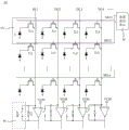
A driving method of a pixel detection circuit. As shown in fig. 1, the pixel detection circuit 01 includes a plurality of detection units 10 defined by gate signal lines (SEL1, SEL2 … …) and read signal lines (DL1, DL2 … …) crossing each other.
The detection unit 10 includes a switching transistor Tc having a gate connected to the gate signal line SEL and a first electrode connected to the read signal line DL. In addition, the above-mentioned detecting unit 10 further includes a photosensor L connected to the second pole of the switching transistor Tc. The photosensor L may collect incident light and photoelectrically convert the collected light signal to output an electrical signal to the read signal line DL.
Preferably, the light sensing device L may be a light emitting diode. In this case, the anode of the light emitting diode is connected to the power supply voltage terminal, and the cathode is connected to the second pole of the switching transistor Tc. The voltage output by the power supply voltage end can drive the light-emitting diode to normally work.
As shown in fig. 2, the parasitic capacitance Cgs between the gate and the source of the switching transistor Tc and the parasitic capacitance cgd between the gate and the drain of the switching transistor Tc have been studied to generate a Clock feed through (Clock feed through) effect and a Charge Injection (Charge Injection) effect when the switching transistor Tc is switched from an off state to an on state or from an on state to an off state, in this case, an extra voltage △ V is superimposed on the signal output terminal Vout, and the extra voltage △ V is shown in table 1.
TABLE 1
When the switch transistor Tc is switched from the OFF state to the ON state, the voltage phi input to the gate of the switch transistor Tc is increased from 0V to Vin-Vth and then to VDD as shown in FIG. 3, and is in an increasing state; or when the on-state is switched to the off-state, the voltage phi input to the gate of the switching transistor Tc is as shown in FIG. 3, and the voltage drops from VDD to Vin-Vth, then to 0V, which is in a falling state.
Specifically, the clock feedthrough effect means that the gate of the switching transistor Tc is connected with a clock signal, and when the transistor is switched from an off state to an on state or from the on state to the off state, the clock signal is coupled to the source or the drain of the switching transistor Tc, so that the signal output by the signal output terminal Vout has an extra voltage, i.e., a feedthrough voltage.
The charge injection effect means that when the switching transistor Tc is turned from an on state to an off state, the channel of the switching transistor Tc discharges charges to the source and the drain, thereby affecting the output signal of the signal output terminal Vout.
Table 1 lists the feedthrough voltage △ V generated by the clock feedthrough effect caused by the parasitic capacitance of the switching transistor Tc in the off state of the switching transistor Tc in both Fast turn-off (Fast turn-off) and Slow turn-off (Slow turn-off) states, and the feedthrough voltage △ V is superimposed on the signal output terminal Vout, thereby affecting the signal output by the signal output terminal Vout.
In this case, the driving method of the pixel detection circuit provided by the embodiment of the present invention includes: in any two adjacent rows of gating signal lines, at the same time, one row of gating signal lines, such as the first row gating signal line SEL1, controls the switching transistor Tc connected with the first row gating signal line SEL1, such as the first row switching transistor Tc1, and is switched from an off state to an on state; another row selection signal line, for example, the second row selection signal line SEL2 controls the switch transistor Tc connected to the second row selection signal line SEL2, for example, the second row switch transistor Tc2 is turned from an on state to an off state.
In the present invention, the type of the switching transistor Tc is not limited, and may be an N-type transistor or a P-type transistor. Taking the above-mentioned switch transistor Tc as an N-type transistor as an example, when the gating signal line SEL controls the switch transistor Tc connected to the gating signal line SEL to switch from the off state to the on state, the voltage supplied to the gate of the switch transistor Tc by the gating signal line SEL tends to increase, for example, from 0V to Vin-Vth in fig. 3, and then to VDD. When the gating signal line SEL controls the switching transistor Tc connected to the gating signal line SEL to switch from the on state to the off state, the gating signal line SEL supplies a falling trend to the gate of the switching transistor Tc, for example, from VDD to Vin-Vth and then to 0V.
In this case, as shown in FIG. 4, the gate voltage of the first row switch transistor Tc1 is rising to make the first row switch transistor Tc1 turn from off to on, at this time, the parasitic capacitance Cp1 of the first row switch transistor Tc1 causes the clock feedthrough effect mentioned above, so that the read signal line DL is overlapped by the positive feedthrough voltage of + △ V.
In addition, the gate voltage of the second row switch transistor Tc2 is decreased to turn the second row switch transistor Tc2 from an on state to an off state, at this time, the parasitic capacitance Cp2 of the second row switch transistor Tc2 causes the clock feedthrough effect, so that a negative feedthrough voltage of- △ V is superimposed on the read signal line DL.
Based on this, for the first row switch transistor Tc1 and the second row switch transistor Tc2 connected to the same read signal line DL, the positive feedthrough voltage + △ V generated by the parasitic capacitance Cp1 of the first row switch transistor Tc1 and the negative feedthrough voltage- △ V generated by the parasitic capacitance Cp2 of the second row switch transistor Tc2 cancel each other out on the read signal line DL, so that the signal output on the read signal line DL is not affected by the feedthrough voltage caused by the parasitic capacitance of the transistor connected to the read signal line DL when the on-state and the off-state are switched.
Next, a specific driving method of the pixel detection circuit shown in fig. 1 will be described in detail with reference to the signal timing chart shown in fig. 5.
Specifically, one driving cycle T includes a first initial time T1, a collection time T2, a second initial time T3, a compensation time T4, and an output end time T5 in this order.
In this case, the driving method further includes:
first, between the first initial time T1 and the acquisition time T2, the nth row, for example, the first row gate signal line SEL1 outputs a high level to control the first row switch transistor Tc1 to be turned on. The read signal line DL supplies a reset voltage, for example, 0V to the first row detecting unit 10. In this case, the voltage remaining in the light emitting diode connected to the first row switching transistor Tc1 is reset by the reset voltage output from the read signal line DL. N is more than or equal to 1 and is a positive integer.
The reset voltage may be provided by a reset voltage terminal Vn provided in the data processor 202 in fig. 7. In addition, taking the pixel detection circuit as an example to detect fingerprint information, the data processor 202 may further compare the voltage output by the reading signal line DL with a preset voltage, and determine whether the touch position of the detection unit 10 providing voltage to the reading signal line DL corresponds to a ridge or a valley of the finger of the user according to the magnitude relationship between the voltage output by the reading signal line DL and the preset voltage. Specifically, since the valley line is lower than the ridge line, the valley line is farther from the light emitting diodes in the detection unit 10, and the ridge line is closer to the light emitting diodes in the detection unit 10. In this case, the reflected light received by the detection unit 10 corresponding to the valley line position is weak, so that the voltage output by the reading signal line DL connected to the detection unit 10 is small; the reflected light received by the detecting unit 10 corresponding to the position of the ridge line is stronger, so that the voltage output by the reading signal line DL connected to the detecting unit 10 is larger.
Based on this, as shown in fig. 6, when the data processor 202 is disposed at an end of the reading signal line DL away from the detecting unit 10, a reset transistor Tr (shown in fig. 7) is disposed between the data processor 202 and the reading signal line DL. The gate of the reset transistor Tr is connected to a reset enable signal terminal RST.
In this case, between the first initial time T1 to the collection time T2, the reset enable signal terminal RST outputs a high level as shown in fig. 5. At this time, the reset transistor Tr described above may electrically connect the read signal line DL with a reset voltage terminal Vn in the data processor 202, and the reset voltage output from the reset voltage terminal Vn is transmitted to the nth row, for example, the first row detecting unit 10, through the read signal line DL.
Next, as shown in fig. 5, between the acquisition time T2 and the compensation time T4, the nth row, for example, the first row gate signal line SEL1 outputs a low level to control the first row switching transistor Tc to be turned off. At this time, the first row of photosensitive elements collects incident optical signals and performs photoelectric conversion.
In addition, between the second initial time T3 and the compensation time T4, the N +1 th row, for example, the second row strobe signal line SEL2 outputs a high level to control the second row switch transistor Tc2 to be turned on. In this case, the read signal line DL supplies the above-described reset voltage, for example, 0V to the second row detecting unit 10. In this case, the voltage remaining in the light emitting diode connected to the second row switching transistor Tc2 is reset by the reset voltage output from the read signal line DL.
Based on this, as described above, when a reset transistor Tr is provided between the data processor 202 and the read signal line DL as shown in fig. 6, the reset enable signal terminal RST outputs a high level as shown in fig. 5 between the second initial time T3 and the compensation time T4. At this time, the reset transistor Tr may electrically connect the read signal line DL with a reset voltage terminal Vn provided in the data processor 202, and the voltage output from the reset voltage terminal Vn is transmitted to the (N + 1) th row, for example, the second row detecting unit 10, through the read signal line DL.
Next, in order to avoid the switching transistor Tc in each of the detection units 10 from generating a feedthrough voltage superimposed on the read signal line DL during the transition between the off state and the on state. Preferably, as shown in fig. 5, at the compensation time T4, the voltage output from the gate signal line SEL2 of the (N + 1) th row, for example, the second row, is in a falling state, so as to control the (N + 1) th row, for example, the second row switch transistor Tc2 to be switched from an on state to an off state.
Meanwhile, at the above-described compensation time T4, the voltage output from the nth row, for example, the first row gate signal line SEL1, assumes a rising state, thereby controlling the nth row, for example, the first row switching transistor Tc1 to be switched from an off state to an on state.
In this case, between the above-mentioned compensation timing T4 and the output end timing T5, since the N +1 th row, for example, the second row switching transistor Tc2 is in the off state, the light signal that can be picked up by the photosensor L in the second row detecting unit 10 is photoelectrically converted.
Further, between the above-described compensation timing T4 and the output end timing T5, since the nth row, for example, the first row switching transistor Tc1 is in the on state, the photosensitive element L in the first row detecting unit 10 outputs the converted electric signal through the reading signal line RL.
The driving periods (T1, T2, T3, T4, and T5) are exemplified by the first row strobe signal line SEL1 and the second row strobe signal line SEL2, and the operation of the switching transistors and the light emitting diodes in the first row detection unit 10 and the second row detection unit 10 is exemplified. The driving process of any two remaining rows of detecting units 10 is the same as that described above, and is not described herein again.
On this basis, in the case that the pixel detection circuit further includes an integrator 201, a sample holder 203, and a digital-to-analog converter 204 as shown in fig. 7, after the photosensor L in the detection unit 10 outputs the converted electric signal through the read signal line RL, the driving method of the pixel detection circuit further includes:
first, the voltage output from the read signal line DL is subjected to accumulation processing by the integrator 201 described above to generate an accumulation voltage and output.
Then, the accumulated voltage output from the integrator 201 is sample-held by the sample-and-hold unit 203 to ensure that the voltage input to the digital-to-analog converter 204 is stable.
Next, the sample-and-hold voltage is analog-to-digital converted, thereby supplying the converted digital voltage to the data processor 202.
It should be noted that the integrator 201, the data processor 202, the sample holder 203, and the digital-to-analog converter 204 may form an acquired signal reading sub-circuit 20(Readout circuit).
As can be seen from the above description, in fig. 7, when the switching transistor Tc is turned from the off state to the on state, the parasitic capacitance Cp of the switching transistor Tc generates the positive feedthrough voltage △ V-VDD × Cp/Cf., and when the switching transistor Tc is turned from the on state to the off state, the parasitic capacitance Cp of the switching transistor Tc generates the negative feedthrough voltage- △ V-VDD × Cp/Cf.
Based on this, as described above, at the compensation time T4 shown in fig. 5, the first row switch transistor Tc1 is turned from off to on, and thus the parasitic capacitance Cp1 of the first row switch transistor Tc1 generates the above-mentioned positive feedthrough voltage △ V, while the second row switch transistor Tc2 is turned from on to off, and thus the parasitic capacitance Cp2 of the second row switch transistor Tc2 generates the above-mentioned negative feedthrough voltage- △ V.
An embodiment of the present invention provides an apparatus for driving the pixel detection circuit 01 by using any one of the driving methods of the pixel detection circuit described above, and as shown in fig. 6, the apparatus includes a gate driving unit 30. The gate driving unit 30 is connected to a gate signal line SEL. The gate driving unit 30 is configured to supply a voltage in an ascending trend to any two adjacent rows of gate signal lines SEL at the same time, for example, a first row gate signal line SEL1, so that the first row switching transistor Tc1 connected to the first row gate signal line SEL1 is switched from an off state to an on state; and supplies a voltage having a falling trend to another row selection signal line SEL, for example, the second row selection signal line SEL2, so that the second row switch transistor Tc2 connected to the second row selection signal line SEL2 is switched from an on state to an off state.
The driving device has the same advantages as the driving method of the pixel detection circuit provided in the foregoing embodiment, and details are not repeated here.
In addition, the driving apparatus further includes a reset unit 40, and the reset unit 40 is connected to the read signal line DL, the reset voltage terminal Vn, and the reset enable signal terminal RST. The reset unit 40 is configured to electrically connect the read signal line RL to the reset voltage terminal Vn under the control of the reset enable signal terminal RST.
The reset unit 40 includes a reset transistor Tr. The reset transistor Tr has a gate connected to a reset enable signal terminal RST, a first pole connected to the read signal line DL, and a second pole connected to a reset voltage terminal RST.
The above description is only for the specific embodiments of the present invention, but the scope of the present invention is not limited thereto, and any person skilled in the art can easily conceive of the changes or substitutions within the technical scope of the present invention, and all the changes or substitutions should be covered within the scope of the present invention. Therefore, the protection scope of the present invention shall be subject to the protection scope of the appended claims.