CN106664095B - digital to analog converter - Google Patents
digital to analog converter Download PDFInfo
- Publication number
- CN106664095B CN106664095B CN201480078271.7A CN201480078271A CN106664095B CN 106664095 B CN106664095 B CN 106664095B CN 201480078271 A CN201480078271 A CN 201480078271A CN 106664095 B CN106664095 B CN 106664095B
- Authority
- CN
- China
- Prior art keywords
- digital
- switches
- input
- terminal
- analog
- Prior art date
- Legal status (The legal status is an assumption and is not a legal conclusion. Google has not performed a legal analysis and makes no representation as to the accuracy of the status listed.)
- Active
Links
Images


Classifications
-
- H—ELECTRICITY
- H03—ELECTRONIC CIRCUITRY
- H03M—CODING; DECODING; CODE CONVERSION IN GENERAL
- H03M1/00—Analogue/digital conversion; Digital/analogue conversion
- H03M1/66—Digital/analogue converters
- H03M1/68—Digital/analogue converters with conversions of different sensitivity, i.e. one conversion relating to the more significant digital bits and another conversion to the less significant bits
-
- H—ELECTRICITY
- H03—ELECTRONIC CIRCUITRY
- H03M—CODING; DECODING; CODE CONVERSION IN GENERAL
- H03M1/00—Analogue/digital conversion; Digital/analogue conversion
- H03M1/66—Digital/analogue converters
- H03M1/74—Simultaneous conversion
- H03M1/76—Simultaneous conversion using switching tree
-
- H—ELECTRICITY
- H03—ELECTRONIC CIRCUITRY
- H03M—CODING; DECODING; CODE CONVERSION IN GENERAL
- H03M1/00—Analogue/digital conversion; Digital/analogue conversion
- H03M1/66—Digital/analogue converters
- H03M1/74—Simultaneous conversion
- H03M1/80—Simultaneous conversion using weighted impedances
- H03M1/808—Simultaneous conversion using weighted impedances using resistors
Landscapes
- Engineering & Computer Science (AREA)
- Theoretical Computer Science (AREA)
- Analogue/Digital Conversion (AREA)
Abstract
Description
背景技术Background technique
数字模拟转换器(DAC)将数字信号或数字转换为模拟电压。在一些实施例中,数字处理器向DAC输出一连串数字,例如二进制数字。DAC将数字转换为模拟信号。例如,在数字音频中,使用数字电子电路处理音频信号,然而,为了被用户听到,数字信号需要转换为模拟信号。A digital-to-analog converter (DAC) converts a digital signal or digital to an analog voltage. In some embodiments, the digital processor outputs a series of numbers, such as binary numbers, to the DAC. A DAC converts digital to analog signals. For example, in digital audio, digital electronic circuits are used to process the audio signal, however, in order to be heard by the user, the digital signal needs to be converted to an analog signal.
因为到DAC的输入信号是具有离散值的数字信号,所以由DAC输出的模拟信号具有离散数量的电压电平。例如,四位DAC可能够接收十六个不同值的输入,该十六个不同值对应于由DAC输出的十六个离散电压电平。一些DAC通过调整到DAC的偏置电压来微调输出电压。这些微调机制需要使用许多电阻器和开关,并且结果,使用DAC上的大的面积。由于与电阻器相关联的寄生电容,所以这些微调机制还使DAC遭受较慢的速度。Because the input signal to the DAC is a digital signal with discrete values, the analog signal output by the DAC has a discrete number of voltage levels. For example, a four-bit DAC may be capable of receiving an input of sixteen different values corresponding to sixteen discrete voltage levels output by the DAC. Some DACs fine-tune the output voltage by adjusting the bias voltage to the DAC. These trimming mechanisms require the use of many resistors and switches and, as a result, use a large area on the DAC. These trimming mechanisms also subject the DAC to slower speeds due to the parasitic capacitances associated with the resistors.
发明内容SUMMARY OF THE INVENTION
一种数字模拟转换器,其具有第一数字模拟阵列和第二数字模拟阵列。第一数字模拟阵列具有参考输入、参考输出、可连接到数字信号的第一数字输入和模拟输出。第二数字模拟阵列包括参考输入、联结到第一数字模拟阵列的参考输入的参考输出,联结到参考输入的多个开关和联结在开关和参考输出之间的多个电阻器。A digital-to-analog converter has a first digital-to-analog array and a second digital-to-analog array. The first digital-to-analog array has a reference input, a reference output, a first digital input connectable to a digital signal, and an analog output. The second digital-analog array includes a reference input, a reference output coupled to the reference input of the first digital-analog array, a plurality of switches coupled to the reference input, and a plurality of resistors coupled between the switches and the reference output.
附图说明Description of drawings
图1是数字模拟转换器的一个实施例的框图。Figure 1 is a block diagram of one embodiment of a digital to analog converter.
图2是图1的第一DAC阵列的一个实施例的示意图。FIG. 2 is a schematic diagram of one embodiment of the first DAC array of FIG. 1 .
图3是具有三位分辨率的图1的第二DAC阵列和第三DAC阵列的实施例的示意图。3 is a schematic diagram of an embodiment of the second and third DAC arrays of FIG. 1 with three-bit resolution.
图4是具有三位分辨率的图1的第二DAC阵列和第三DAC阵列的另一个实施例的示意图。FIG. 4 is a schematic diagram of another embodiment of the second and third DAC arrays of FIG. 1 with three bits of resolution.
图5是具有二位分辨率的图1的第二DAC阵列和第三DAC阵列的另一个实施例的示意图。5 is a schematic diagram of another embodiment of the second and third DAC arrays of FIG. 1 with two-bit resolution.
图6是具有二位分辨率的图1的第二DAC阵列和第三DAC阵列的另一个实施例的示意图。6 is a schematic diagram of another embodiment of the second and third DAC arrays of FIG. 1 with two-bit resolution.
图7是具有二位分辨率的图1的第二DAC阵列和第三DAC阵列的另一个实施例的示意图。7 is a schematic diagram of another embodiment of the second and third DAC arrays of FIG. 1 with two-bit resolution.
具体实施方式Detailed ways
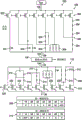
本文中描述了与常规的DAC相比使用更少的面积的数字模拟转换器(DAC)。DAC将数字信号或数字转换为模拟电压。例如,向DAC输入二进制数字。DAC对二进制数字进行解码,并且输出代表该二进制数字的电压。一些DAC具有使得DAC能够微调模拟输出的模块。参考图1,图1是具有多个阵列102的DAC 100的一个实施例的框图。阵列102被各自称为第一DAC阵列106、第二DAC阵列108和第三DAC阵列110。第二DAC阵列108有时被称为顶部阵列108,并且第三DAC阵列110有时被称为底部阵列110。在一些实施例中,第一DAC阵列106被称为粗略DAC阵列,并且第二DAC阵列108和第三DAC阵列110被称为精细阵列。Digital-to-analog converters (DACs) that use less area than conventional DACs are described herein. A DAC converts a digital signal or digital to an analog voltage. For example, input a binary number to a DAC. The DAC decodes a binary number and outputs a voltage representing the binary number. Some DACs have blocks that allow the DAC to fine-tune the analog output. Referring to FIG. 1 , FIG. 1 is a block diagram of one embodiment of a
第一DAC阵列106具有有时被称为第一数字输入114的数字输入114。数字输入114联结到或能够联结到将转换为模拟信号的数字信号,该模拟信号在输出116上输出。第一DAC阵列106具有有时被分别地称为第一参考输入120和第一参考输出122的参考输入120和参考输出122。如下面更详细描述的,第一参考输入120和第一参考输出122微调由第一DAC阵列106输出的模拟电压值。通过用如下面描述的偏移电压偏置第一DAC阵列106实现微调。The
第二DAC阵列108具有有时被分别地称为第二电压参考输入126和第二电压参考输出128的电压参考输入126和电压参考输出128。在图1的实施例中,第二电压参考输入126连接到是直流电压的电压参考Vref。第二参考输出128连接到第一DAC阵列106的参考输入120。第二DAC阵列108还具有有时被称为第二数字输入130的数字输入130。如下面更详细描述的,第二数字输入130能够联结到或联结到数字信号。总的来说,由第二数字输入130输入的数字信号是第一数字输入114上的数字信号的一个或更多个最低有效位,或较低有效位。由第二DAC阵列108使用第二数字输入130,以在参考输入120处生成偏移电压,并且第二数字输入130被用于微调模拟输出的值。The
第三DAC阵列110具有有时被分别地称为第三参考输入134和第三参考输出136的参考输入134和参考输出136。参考输入134连接到第一DAC阵列106的参考输出122。参考输出136联结到或能够联结到第二参考电压,在图1的实施例中该第二参考电压接地,作为电压参考Vref。第三DAC阵列110具有有时被称为第三数字输入140的数字输入140。如下面更详细描述的,第三数字输入140联结到或能够联结到数字信号。总的来说,第三DAC阵列110与第二DAC阵列108一起工作来微调由第一DAC阵列106输出的模拟信号的值。与第二DAC阵列108一样,由第三数字输入140输入的数字信号是第一数字输入114上的数字信号的一个或更多个最低有效位,或较低有效位。The
参考图2,图2是图1的DAC 100的一个实施例的示意图。在图2的示意图中,第一DAC阵列106被示出为常规的数字模拟转换器,并且第二DAC阵列108和第三DAC阵列110被示出为框。输入由A0-A5的输入信号部分指定的数字信号。较高位A2-A5输入到解码器200和解码器202,解码器200和解码器202对数字信号中的位进行解码以操作多个开关154,多个开关154在图2的实施例中是场效应晶体管(FET)。在图2的实施例中,解码器200和解码器202是2×4解码器。数字信号的最低有效位输入解码器208,解码器208在图1的实施例中是3×8解码器。在其他实施例中,可使用其他解码器。例如,可使用2×4解码器。解码器208对数字信号的最低有效位进行解码以操作第二DAC阵列108和第三DAC阵列110。在图2中描述的实施例中,解码器208输出能够表示由第二DAC阵列108和第三DAC阵列110生成的总共八个不同的精细电压的三个位。在一些实施例中,DAC 100具有可提供内插的缓冲器230。Referring to FIG. 2 , FIG. 2 is a schematic diagram of one embodiment of the
图3示出第二DAC阵列108和第三DAC阵列110的实施例以及表示第一DAC阵列106的框的示意图。第二DAC阵列108和第三DAC阵列110包括在网络中的电阻器以提供离散电阻值,其中第二DAC阵列108的电阻器网络是在第三DAC阵列110中的电阻器网络的倒置或镜像。因为最低有效位被用于控制第二DAC阵列108和第三DAC阵列110,所以如将由以下描述明显的,有八个离散电阻值用于微调阵列108和阵列110的可能性。在其他实施例中,不同数量的最低有效位可被用于生成不同数量的可能的离散电阻值。FIG. 3 shows an embodiment of the
第二DAC阵列108包括网络300。网络300包括由标记A-标记G和开关303指定的八个开关302。开关302将电阻器304连接到参考输入126,参考输入126将电阻器304连接到参考电压VREF。在本文描述的实施例中,电阻器304全部具有相同值,指定该值为R。开关303总是导通,并且开关303可由导体来代替,导体诸如导线或迹线,使得电阻器R3连接在参考输入126和参考输出128之间。开关A-开关G设置在参考输入126和参考输出128之间的电阻值。如图3所示,在参考输入126和参考输出128之间的电阻至少部分地控制到第一DAC阵列106的参考输入120的电压。电阻值以八分之一R为增量,其遵从由图2的解码器208输出的三个位。The
由与电阻器相关联的开关引用该电阻器。例如,开关A与电阻器R1和R2相关联。因此,当开关A闭合时,在输入参考126和输出参考128之间的电阻是电阻器R1至电阻器R3的并联电阻,其中R3与开关303相关联。表306提供关于开关设置的图表,以实现增量电阻值。通过闭合在表306中指示的开关,实现八分之一R的增量电阻值。The resistor is referenced by the switch associated with the resistor. For example, switch A is associated with resistors R1 and R2. Thus, when switch A is closed, the resistance between
第三DAC阵列110具有大体上类似于第二DAC阵列108的电阻器和开关网络300的电阻器和开关网络308。第三DAC阵列110的电阻器和开关网络308有时被称为是第二DAC阵列108的电阻器和开关网络300的倒置或镜像。如图3所示,第三DAC阵列110具有多个电阻器310和开关312。开关312被指定为开关A-开关H和开关320,其中开关320总是导通的。开关320可由导体(诸如导线或迹线)替换,而不是由图3中所示的FET替换,使得电阻器R4总是连接在参考输入134和参考输出136之间。The
第三DAC阵列110经配置,使得电阻器310连接或以其它方式联结到参考输入134,并且开关312连接或以其他方式联结到参考输出136。电阻器310和开关312的网络308经配置是倒置或镜像网络300。网络308的开关和电阻配置提供如由表310所示的0至7/8R的电阻值。因为网络308的开关320连接在参考输入134和参考输出136之间,没有电阻器连接在线路中,所以该配置与网络300的配置稍微不同。因此,当开关320闭合时,参考输入134短接到参考输出136,并且在参考输入134和参考输出136之间没有电压降。The
已经描述了第二DAC阵列108和第三DAC阵列110的配置,现在将描述第二DAC阵列108和第三DAC阵列110的操作。如上所述,第二DAC阵列108和第三DAC阵列110具有可变的电阻值,并且因此能够调整在第一DAC阵列106上的参考输入120和参考输出122之间的电压降。通过调整电压降,能够增大或减小在模拟输出处的电压。在本文描述的实施例中,在第二DAC阵列108和第三DAC阵列110之间的累积电阻维持在R的值。Having described the configuration of the
作为DAC 100的操作的一个示例,LSB指示第一阵列106的模拟输出的电压需要显著上升或具有显著的正偏移。图2的解码器208生成数字信号,以达到该数字信号被输出到第二DAC阵列108和第三DAC阵列110两者的效果。发送到第二DAC阵列108的数字信号将降低其电阻。在本文描述的示例中,第二DAC阵列108的电阻需要下降至(1/8)R,这通过闭合开关A、开关C和开关E实现,如表306所示的。同样地,第三DAC阵列110的电阻将增大到其最大量(7/8)R,这通过闭合开关H实现,如表310所示的。从而,模拟输出电压上移了第一阵列106的一个LSB电压的7/8。在第一DAC阵列108和第二DAC阵列110之间的累积电阻保持在R。因此,在第一阵列106的一个LSB电压内实现显著的偏移。当需要其他偏移时,能够设置开关300和开关312的其他配置。As an example of the operation of the
在一些实施例中,正偏移或负偏移可被施加到模拟输出的电压。在这些实施例中,用第二DAC阵列108和第三DAC阵列110的电阻值中的每个为R/2正常地设置DAC 100。在图3的实施例中,通过接通第二DAC阵列108中的开关C和接通第三DAC阵列110中的开关D来满足该正常条件。如果需要正偏移,则减小第二DAC阵列108中的电阻,并且增大第三DAC阵列110中的电阻。另一方面,如果需要负偏移,则增大第二DAC阵列108中的电阻,并且减小第三DAC阵列110中的电阻。In some embodiments, a positive offset or a negative offset can be applied to the voltage of the analog output. In these embodiments,
在图4中示出第二DAC阵列108和第三DAC阵列110的另一个实施例。第二DAC阵列108具有电阻器402和开关404的网络400。在图4的实施例中,有被标记为开关A-开关I的九个开关。根据表404设置开关404以产生在参考输入126和参考输出128之间的电阻值。因为第二DAC阵列108使用九个开关,所以需要九个位来操作开关404以获得以(1/8)R的值增加的电阻值。在图4的实施例中,全部的电阻器402具有相同值,该值被称为R。Another embodiment of the
第三DAC阵列110具有电阻器412和开关414的网络410,该网络410类似于第二DAC阵列108的网络400。网络410被称为是网络400的倒置或被称为是网络400的镜像。第二DAC阵列108的开关404连接到或联结到参考输入126,其中第三DAC阵列110的开关414连接到或联结到参考输出136。同样地,第二DAC阵列108的电阻器402连接到或联结到参考输出128,并且第三DAC阵列110的电阻器412连接到或联结到参考输入134。一个例外是开关J,开关J连接在参考输入134和参考输出136之间。The
图3和图4的DAC阵列108、DAC阵列110在参考输入126、参考输入134和参考输出128、参考输出136之间提供八个电阻值。电阻值以电阻值R的八分之一为增量。电阻值的数量对应于由图2的解码器208生成的数字信号,该数字信号具有对应于值8的三个位。在其他实施例中,使用更多数量或更少数量的位。The
参考图5,图5示出提供在参考输入126、参考输入134和参考输出128、参考输出136之间的四个不同的电阻值的可能性的网络500和网络502的实施例。该四个不同电阻值对应于由图2的解码器208生成的两个位。网络500具有连接在参考输入126和电阻器512之间的四个开关510。电阻器512或直接地或通过与其他电阻器的串联连接来连接到参考输出128。网络502使用连接在电阻器522和参考输出136之间的四个开关520。当网络502中的附加开关524闭合时,网络502中的附加开关524将参考输入134短接到参考输出136。网络500被称为是网络502的镜像。Referring to FIG. 5, FIG. 5 shows embodiments of
图6示出提供在参考输入126、参考输入134和参考输出128、参考输出136之间的四个不同的电阻值的可能性的网络600和网络602的其他的实施例。该四个不同电阻值对应于由图2的解码器208生成的两个位。网络600具有连接在参考输入126和电阻器612之间的四个开关610。电阻器612或直接地或通过与其他电阻器的串联连接来连接到参考输出128。网络602使用连接在电阻器622和参考输出136之间的四个开关620。当网络602中的附加开关624闭合时,网络602中的附加开关624将输入参考134短接到输出参考136。网络600有时被称为是网络602的镜像。FIG. 6 shows other embodiments of
图7还示出提供在参考输入126、参考输入134和参考输出128、参考输出136之间的四个不同的电阻值的可能性的网络700和网络702的其他的实施例。与图5和图6的网络一样,该四个不同电阻值对应于由图2的解码器208生成的两个位。网络700具有连接在参考输入126和电阻器712之间的四个开关710。电阻器712或直接地或通过与其他电阻器的串联连接来连接到参考输出128。网络702使用连接在电阻器722和参考输出136之间的四个开关720。当网络602中的附加开关724闭合时,网络602中的附加开关724将参考输入134短接到参考输出136。网络700被称为是网络702的镜像。FIG. 7 also shows other embodiments of
已经描述第二DAC阵列108和第三DAC阵列110的实施例,现在将描述其他实施例。上述实施例使用第二DAC阵列108和第三DAC阵列110中的网络的镜像。在一些实施例中,不需要镜像。例如,在第二DAC阵列108中可使用网络600,并且在第三DAC阵列110中可使用网络702。该实施例确实需要图2的解码器208来输出不同的位以对应于不同的网络模式。Having described embodiments of the
上面所公开的第二DAC阵列108中的网络全部具有连接在参考输入126和参考输出128之间的最小电阻。例如最小电阻可以是R/8或R/4。该最小电阻防止电压VREF直接施加到第一DAC阵列106的输入参考120,这减少模拟信号的饱和的可能性。The networks in the
以上公开的第三DAC阵列110中的网络全部具有使得参考输入134能够被短接到参考输出136或直接地连接到参考输出136的开关。在参考输出136接地的实施例中,该开关有效地为第一DAC阵列106的参考输出122提供接地参考。The networks in the
在以上描述的网络中的许多网络中,与常规的电阻器网络相比,仅使用大约电阻器的四分之一。结果是由网络使用的面积仅仅是常规网络的大小的四分之一。通过不同电阻器之间的串联或并联连接实现电阻器数量的降低。应当注意,在以上描述的全部的网络中,有连接到并联连接的电阻器的至少一个开关,其中并联的电阻器连接到参考输出128或参考输入134。另外,每个网络具有连接到单个电阻器的开关,该单个电阻器连接到参考输出128或参考输入134。In many of the networks described above, only about a quarter of the resistors are used compared to conventional resistor networks. The result is that the area used by the network is only a quarter of the size of a conventional network. The reduction in the number of resistors is achieved by connecting the different resistors in series or in parallel. It should be noted that in all of the networks described above, there is at least one switch connected to parallel connected resistors connected to either the
虽然本文已经详细描述了说明性的和目前优选的实施例,但是应该理解本发明概念可以多种其它方式体现和采用,并且所附权利要求书旨在被解释为包括此类变化,除非此类变化在由现有技术限制的范围内。While illustrative and presently preferred embodiments have been described in detail herein, it should be understood that the inventive concept may be embodied and employed in various other ways and the appended claims are intended to be construed to include such changes, unless such changes are Variations are within limits limited by the prior art.
Claims (20)
Applications Claiming Priority (1)
| Application Number | Priority Date | Filing Date | Title |
|---|---|---|---|
| PCT/CN2014/076838 WO2015168854A1 (en) | 2014-05-06 | 2014-05-06 | Digital to analog converter |
Publications (2)
| Publication Number | Publication Date |
|---|---|
| CN106664095A CN106664095A (en) | 2017-05-10 |
| CN106664095B true CN106664095B (en) | 2020-06-30 |
Family
ID=54391948
Family Applications (1)
| Application Number | Title | Priority Date | Filing Date |
|---|---|---|---|
| CN201480078271.7A Active CN106664095B (en) | 2014-05-06 | 2014-05-06 | digital to analog converter |
Country Status (4)
| Country | Link |
|---|---|
| US (1) | US9866235B2 (en) |
| JP (1) | JP6643560B2 (en) |
| CN (1) | CN106664095B (en) |
| WO (1) | WO2015168854A1 (en) |
Families Citing this family (3)
| Publication number | Priority date | Publication date | Assignee | Title |
|---|---|---|---|---|
| EP3566310B1 (en) * | 2017-01-06 | 2025-05-14 | Texas Instruments Incorporated | Area efficient digital to analog and analog to digital converters |
| CN109391270B (en) * | 2017-08-08 | 2023-09-26 | 恩智浦美国有限公司 | Digital-to-analog converter (DAC) with sub-DAC containing resistor array |
| CN116401199B (en) * | 2023-06-09 | 2024-03-05 | 珠海智融科技股份有限公司 | Signal conversion circuit, transmission method, device, electronic apparatus, and storage medium |
Citations (4)
| Publication number | Priority date | Publication date | Assignee | Title |
|---|---|---|---|---|
| EP0982847A1 (en) * | 1998-08-20 | 2000-03-01 | Sony Corporation | Detection circuit |
| CN1558449A (en) * | 2004-02-11 | 2004-12-29 | 复旦大学 | Programmable Digital-Analog Mixed Device Architecture |
| CN1913364A (en) * | 2005-08-08 | 2007-02-14 | 三星电机株式会社 | Digital/analog converter |
| CN101207385A (en) * | 2006-12-22 | 2008-06-25 | 美格纳半导体有限会社 | Digital-to-analog converter and digital-to-analog conversion method thereof |
Family Cites Families (17)
| Publication number | Priority date | Publication date | Assignee | Title |
|---|---|---|---|---|
| US3703956A (en) * | 1971-02-16 | 1972-11-28 | Cato Oil & Grease Co | Oil change kit |
| US5617091A (en) * | 1994-09-02 | 1997-04-01 | Lowe, Price, Leblanc & Becker | Resistance ladder, D-A converter, and A-D converter |
| JPH08125536A (en) * | 1994-09-02 | 1996-05-17 | Mitsubishi Electric Corp | Resistance ladder, D-A converter, and A-D converter |
| US5646619A (en) * | 1995-04-26 | 1997-07-08 | Lucent Technologies Inc. | Self-calibrating high speed D/A converter |
| JPH1041824A (en) * | 1996-07-26 | 1998-02-13 | Mitsubishi Electric Corp | D / A converter and A / D converter |
| US6307490B1 (en) * | 1999-09-30 | 2001-10-23 | The Engineering Consortium, Inc. | Digital to analog converter trim apparatus and method |
| US6201491B1 (en) * | 2000-01-26 | 2001-03-13 | Microchip Technology Incorporated | Digitally switched potentiometer having improved linearity and settling time |
| DE60307039T2 (en) * | 2003-03-14 | 2007-01-18 | Stmicroelectronics S.R.L., Agrate Brianza | High-resolution digital-to-analog converter with low power consumption |
| US6738006B1 (en) * | 2003-05-06 | 2004-05-18 | Analog Devices, Inc. | Digital/analog converter including gain control for a sub-digital/analog converter |
| KR20060017819A (en) * | 2003-05-27 | 2006-02-27 | 조지아 테크 리서치 코오포레이션 | Floating gate reference circuit |
| JP4934953B2 (en) * | 2004-09-28 | 2012-05-23 | ソニー株式会社 | Current output type drive circuit and electronic device |
| CN100590981C (en) * | 2006-04-12 | 2010-02-17 | 曹先国 | Digital to Analog Converter |
| US7868795B2 (en) * | 2008-09-30 | 2011-01-11 | Freescale Semiconductor, Inc. | Data conversion circuitry with an extra successive approximation step and method therefor |
| US7884747B2 (en) * | 2009-06-12 | 2011-02-08 | Analog Devices, Inc. | Digital to analog converters having circuit architectures to overcome switch losses |
| CN102118172B (en) | 2009-12-31 | 2014-07-30 | 意法半导体研发(上海)有限公司 | Device and method for simplifying digital-to-analogue converter circuit by using Gray code |
| CN102377434B (en) | 2010-08-04 | 2015-04-22 | 意法半导体研发(上海)有限公司 | Coarse digital-to-analog converter architecture for voltage interpolation DAC (digital-to-analog converter) |
| US8823569B2 (en) * | 2012-12-18 | 2014-09-02 | Julian Jenkins | Digital-to-analog converter |
-
2014
- 2014-05-06 JP JP2016566979A patent/JP6643560B2/en active Active
- 2014-05-06 CN CN201480078271.7A patent/CN106664095B/en active Active
- 2014-05-06 WO PCT/CN2014/076838 patent/WO2015168854A1/en not_active Ceased
- 2014-05-06 US US14/482,734 patent/US9866235B2/en active Active
Patent Citations (4)
| Publication number | Priority date | Publication date | Assignee | Title |
|---|---|---|---|---|
| EP0982847A1 (en) * | 1998-08-20 | 2000-03-01 | Sony Corporation | Detection circuit |
| CN1558449A (en) * | 2004-02-11 | 2004-12-29 | 复旦大学 | Programmable Digital-Analog Mixed Device Architecture |
| CN1913364A (en) * | 2005-08-08 | 2007-02-14 | 三星电机株式会社 | Digital/analog converter |
| CN101207385A (en) * | 2006-12-22 | 2008-06-25 | 美格纳半导体有限会社 | Digital-to-analog converter and digital-to-analog conversion method thereof |
Also Published As
| Publication number | Publication date |
|---|---|
| US9866235B2 (en) | 2018-01-09 |
| US20170194981A1 (en) | 2017-07-06 |
| CN106664095A (en) | 2017-05-10 |
| JP6643560B2 (en) | 2020-02-12 |
| WO2015168854A1 (en) | 2015-11-12 |
| JP2017515419A (en) | 2017-06-08 |
Similar Documents
| Publication | Publication Date | Title |
|---|---|---|
| US9991900B1 (en) | Digital to analog (DAC) converter with current calibration | |
| JP3986970B2 (en) | D / A converter | |
| US6703956B1 (en) | Technique for improved linearity of high-precision, low-current digital-to-analog converters | |
| CN106664096B (en) | Hybrid digital/analog conversion system | |
| US8089383B2 (en) | Programmable digital-to-analog converter | |
| JP3534179B2 (en) | Digital / analog converter | |
| US10790848B2 (en) | Segmented resistive digital to analog converter | |
| JP2001244816A (en) | Digitally switched potentiometer with improved linearity and settling time | |
| WO2013165976A2 (en) | Segmented digital-to-analog converter having weighted current sources | |
| CN106664095B (en) | digital to analog converter | |
| US10511321B2 (en) | Digital-to-analog converter and method for digital-to-analog conversion | |
| US20060132343A1 (en) | High speed differential resistive voltage digital-to-analog converter | |
| US20200212860A1 (en) | Voltage detection circuit | |
| CN111801894B (en) | Digital-to-analog converter system | |
| US9800259B1 (en) | Digital to analog converter for performing digital to analog conversion with current source arrays | |
| US10084465B2 (en) | Analog-to-digital converters with a plurality of comparators | |
| US20090079609A1 (en) | Digital-to-analog converter | |
| US9621181B2 (en) | Digital to analog converter with output impedance compensation | |
| US20160233878A1 (en) | Current output circuit | |
| JPH09232961A (en) | D / A converter | |
| JP2007336540A (en) | Digital to analog converter | |
| JP4158731B2 (en) | Ladder resistance type D / A conversion circuit | |
| CN106253898B (en) | Apparatus for gain selection with parasitic element compensation and related methods | |
| JP2003309469A (en) | Semiconductor integrated circuit | |
| KR101749173B1 (en) | Segmented digital analog converter reducing layout area |
Legal Events
| Date | Code | Title | Description |
|---|---|---|---|
| PB01 | Publication | ||
| PB01 | Publication | ||
| SE01 | Entry into force of request for substantive examination | ||
| SE01 | Entry into force of request for substantive examination | ||
| GR01 | Patent grant | ||
| GR01 | Patent grant |