CN100583210C - Driving circuit and method for active matrix organic light emitting diode device - Google Patents
Driving circuit and method for active matrix organic light emitting diode device Download PDFInfo
- Publication number
- CN100583210C CN100583210C CN200510082442A CN200510082442A CN100583210C CN 100583210 C CN100583210 C CN 100583210C CN 200510082442 A CN200510082442 A CN 200510082442A CN 200510082442 A CN200510082442 A CN 200510082442A CN 100583210 C CN100583210 C CN 100583210C
- Authority
- CN
- China
- Prior art keywords
- thin film
- film transistor
- switching thin
- driving
- coupled
- Prior art date
- Legal status (The legal status is an assumption and is not a legal conclusion. Google has not performed a legal analysis and makes no representation as to the accuracy of the status listed.)
- Expired - Lifetime
Links
Images


Classifications
-
- G—PHYSICS
- G09—EDUCATION; CRYPTOGRAPHY; DISPLAY; ADVERTISING; SEALS
- G09G—ARRANGEMENTS OR CIRCUITS FOR CONTROL OF INDICATING DEVICES USING STATIC MEANS TO PRESENT VARIABLE INFORMATION
- G09G3/00—Control arrangements or circuits, of interest only in connection with visual indicators other than cathode-ray tubes
- G09G3/20—Control arrangements or circuits, of interest only in connection with visual indicators other than cathode-ray tubes for presentation of an assembly of a number of characters, e.g. a page, by composing the assembly by combination of individual elements arranged in a matrix no fixed position being assigned to or needed to be assigned to the individual characters or partial characters
- G09G3/22—Control arrangements or circuits, of interest only in connection with visual indicators other than cathode-ray tubes for presentation of an assembly of a number of characters, e.g. a page, by composing the assembly by combination of individual elements arranged in a matrix no fixed position being assigned to or needed to be assigned to the individual characters or partial characters using controlled light sources
- G09G3/30—Control arrangements or circuits, of interest only in connection with visual indicators other than cathode-ray tubes for presentation of an assembly of a number of characters, e.g. a page, by composing the assembly by combination of individual elements arranged in a matrix no fixed position being assigned to or needed to be assigned to the individual characters or partial characters using controlled light sources using electroluminescent panels
- G09G3/32—Control arrangements or circuits, of interest only in connection with visual indicators other than cathode-ray tubes for presentation of an assembly of a number of characters, e.g. a page, by composing the assembly by combination of individual elements arranged in a matrix no fixed position being assigned to or needed to be assigned to the individual characters or partial characters using controlled light sources using electroluminescent panels semiconductive, e.g. using light-emitting diodes [LED]
- G09G3/3208—Control arrangements or circuits, of interest only in connection with visual indicators other than cathode-ray tubes for presentation of an assembly of a number of characters, e.g. a page, by composing the assembly by combination of individual elements arranged in a matrix no fixed position being assigned to or needed to be assigned to the individual characters or partial characters using controlled light sources using electroluminescent panels semiconductive, e.g. using light-emitting diodes [LED] organic, e.g. using organic light-emitting diodes [OLED]
- G09G3/3225—Control arrangements or circuits, of interest only in connection with visual indicators other than cathode-ray tubes for presentation of an assembly of a number of characters, e.g. a page, by composing the assembly by combination of individual elements arranged in a matrix no fixed position being assigned to or needed to be assigned to the individual characters or partial characters using controlled light sources using electroluminescent panels semiconductive, e.g. using light-emitting diodes [LED] organic, e.g. using organic light-emitting diodes [OLED] using an active matrix
- G09G3/3233—Control arrangements or circuits, of interest only in connection with visual indicators other than cathode-ray tubes for presentation of an assembly of a number of characters, e.g. a page, by composing the assembly by combination of individual elements arranged in a matrix no fixed position being assigned to or needed to be assigned to the individual characters or partial characters using controlled light sources using electroluminescent panels semiconductive, e.g. using light-emitting diodes [LED] organic, e.g. using organic light-emitting diodes [OLED] using an active matrix with pixel circuitry controlling the current through the light-emitting element
-
- G—PHYSICS
- G09—EDUCATION; CRYPTOGRAPHY; DISPLAY; ADVERTISING; SEALS
- G09G—ARRANGEMENTS OR CIRCUITS FOR CONTROL OF INDICATING DEVICES USING STATIC MEANS TO PRESENT VARIABLE INFORMATION
- G09G2300/00—Aspects of the constitution of display devices
- G09G2300/04—Structural and physical details of display devices
- G09G2300/0404—Matrix technologies
- G09G2300/0417—Special arrangements specific to the use of low carrier mobility technology
-
- G—PHYSICS
- G09—EDUCATION; CRYPTOGRAPHY; DISPLAY; ADVERTISING; SEALS
- G09G—ARRANGEMENTS OR CIRCUITS FOR CONTROL OF INDICATING DEVICES USING STATIC MEANS TO PRESENT VARIABLE INFORMATION
- G09G2300/00—Aspects of the constitution of display devices
- G09G2300/04—Structural and physical details of display devices
- G09G2300/0421—Structural details of the set of electrodes
- G09G2300/043—Compensation electrodes or other additional electrodes in matrix displays related to distortions or compensation signals, e.g. for modifying TFT threshold voltage in column driver
-
- G—PHYSICS
- G09—EDUCATION; CRYPTOGRAPHY; DISPLAY; ADVERTISING; SEALS
- G09G—ARRANGEMENTS OR CIRCUITS FOR CONTROL OF INDICATING DEVICES USING STATIC MEANS TO PRESENT VARIABLE INFORMATION
- G09G2300/00—Aspects of the constitution of display devices
- G09G2300/08—Active matrix structure, i.e. with use of active elements, inclusive of non-linear two terminal elements, in the pixels together with light emitting or modulating elements
- G09G2300/0809—Several active elements per pixel in active matrix panels
- G09G2300/0819—Several active elements per pixel in active matrix panels used for counteracting undesired variations, e.g. feedback or autozeroing
-
- G—PHYSICS
- G09—EDUCATION; CRYPTOGRAPHY; DISPLAY; ADVERTISING; SEALS
- G09G—ARRANGEMENTS OR CIRCUITS FOR CONTROL OF INDICATING DEVICES USING STATIC MEANS TO PRESENT VARIABLE INFORMATION
- G09G2300/00—Aspects of the constitution of display devices
- G09G2300/08—Active matrix structure, i.e. with use of active elements, inclusive of non-linear two terminal elements, in the pixels together with light emitting or modulating elements
- G09G2300/0809—Several active elements per pixel in active matrix panels
- G09G2300/0842—Several active elements per pixel in active matrix panels forming a memory circuit, e.g. a dynamic memory with one capacitor
- G09G2300/0861—Several active elements per pixel in active matrix panels forming a memory circuit, e.g. a dynamic memory with one capacitor with additional control of the display period without amending the charge stored in a pixel memory, e.g. by means of additional select electrodes
-
- G—PHYSICS
- G09—EDUCATION; CRYPTOGRAPHY; DISPLAY; ADVERTISING; SEALS
- G09G—ARRANGEMENTS OR CIRCUITS FOR CONTROL OF INDICATING DEVICES USING STATIC MEANS TO PRESENT VARIABLE INFORMATION
- G09G2310/00—Command of the display device
- G09G2310/02—Addressing, scanning or driving the display screen or processing steps related thereto
- G09G2310/0262—The addressing of the pixel, in a display other than an active matrix LCD, involving the control of two or more scan electrodes or two or more data electrodes, e.g. pixel voltage dependent on signals of two data electrodes
-
- G—PHYSICS
- G09—EDUCATION; CRYPTOGRAPHY; DISPLAY; ADVERTISING; SEALS
- G09G—ARRANGEMENTS OR CIRCUITS FOR CONTROL OF INDICATING DEVICES USING STATIC MEANS TO PRESENT VARIABLE INFORMATION
- G09G2320/00—Control of display operating conditions
- G09G2320/02—Improving the quality of display appearance
- G09G2320/0242—Compensation of deficiencies in the appearance of colours
Landscapes
- Engineering & Computer Science (AREA)
- Physics & Mathematics (AREA)
- Computer Hardware Design (AREA)
- General Physics & Mathematics (AREA)
- Theoretical Computer Science (AREA)
- Electroluminescent Light Sources (AREA)
- Control Of Indicators Other Than Cathode Ray Tubes (AREA)
Abstract
公开了一种用于有机发光二极管器件的驱动电路和驱动方法。该有机发光二极管器件的驱动电路包括多个RGB像素,该多个RGB像素中的每一个包括:沿第一方向设置的选通线,以及沿与该第一方向交叉的第二方向设置的数据线和电源线;与所述选通线和所述数据线交叉的区域相连的多个开关薄膜晶体管;与所述开关薄膜晶体管和所述电源线相连的存储电容器;与所述存储电容器和所述电源线相连的驱动薄膜晶体管;与所述驱动薄膜晶体管相连的有机发光二极管;与所述多个开关薄膜晶体管之一相连的可变电压部分;以及与所述多个开关薄膜晶体管中的至少一个相连的SELECT部分,其中所述可变电压部分独立地连接到所述多个RGB像素。
Disclosed are a driving circuit and a driving method for an organic light emitting diode device. The driving circuit of the organic light emitting diode device includes a plurality of RGB pixels, each of the plurality of RGB pixels includes: a gate line arranged along a first direction, and a data line arranged along a second direction crossing the first direction line and power line; a plurality of switching thin film transistors connected to the crossing area of the gate line and the data line; a storage capacitor connected to the switching thin film transistor and the power line; connecting the storage capacitor and the A driving thin film transistor connected to the power supply line; an organic light emitting diode connected to the driving thin film transistor; a variable voltage part connected to one of the plurality of switching thin film transistors; and at least one of the plurality of switching thin film transistors a connected SELECT section, wherein said variable voltage section is independently connected to said plurality of RGB pixels.
Description
技术领域 technical field
本发明涉及有源矩阵型有机发光二极管器件的驱动电路,更具体地,涉及有源矩阵型有机发光二极管器件的驱动电路和驱动方法,其可以通过对位于有机发光二极管器件之间的多晶硅薄膜晶体管的阈值电压的变化进行补偿,来改善显示板之间的亮度均匀性。The present invention relates to a driving circuit of an active matrix organic light emitting diode device, and more particularly, to a driving circuit and a driving method of an active matrix organic light emitting diode device, which can be achieved by controlling polysilicon thin film transistors located between the organic light emitting diode devices Variations in threshold voltage are compensated to improve brightness uniformity between panels.
背景技术 Background technique
近年来,由于其重量轻、功耗低的优点,而使得液晶显示器件(LCD)成为目前最常用的一种平板显示器(FPD)。In recent years, liquid crystal display (LCD) has become the most commonly used type of flat panel display (FPD) due to its advantages of light weight and low power consumption.
然而,液晶显示器件不是自发光元件,而是光接收元件,并且具有亮度、对比度、视角、大尺寸等方面的技术限制。因此,近年来,已积极努力地开发了新型的平板显示器,以克服这种缺点。However, liquid crystal display devices are not self-emitting elements but light-receiving elements, and have technical limitations in terms of brightness, contrast, viewing angle, large size, and the like. Therefore, in recent years, vigorous efforts have been made to develop new flat panel displays to overcome such disadvantages.
作为新型平板显示器之一,有机发光二极管由于是自发光型,所以在视角、对比度等方面优于液晶显示器,并且可以将其制造为重量轻并且薄的类型,并且由于其不需要背光,所以其在功耗方面具有优势。As one of the new flat panel displays, organic light-emitting diodes are superior to liquid crystal displays in terms of viewing angle, contrast ratio, etc. because they are self-illuminating type, and can be manufactured as light-weight and thin types, and since they do not require a backlight, their Advantages in terms of power consumption.
此外,有机发光二极管还具有以下优点:其对于外部冲击非常坚固,并且因为其能够采用直流低压驱动,所以可以提供宽的温度范围,其具有快的响应速度,并且完全制成为固相,尤其是其制造成本低廉。In addition, organic light-emitting diodes also have the advantages that they are very robust against external shocks, can provide a wide temperature range because they can be driven with DC low voltage, have a fast response speed, and are completely made into a solid phase, especially It is cheap to manufacture.
特别地,在有机发光二极管器件的制造工艺中,仅需要淀积和封装设备,而不象液晶显示器件和PDP(等离子体显示板)那样,因此,该工艺非常简单。In particular, in the manufacturing process of the organic light emitting diode device, only deposition and packaging equipment are required, unlike liquid crystal display devices and PDP (Plasma Display Panel), and thus, the process is very simple.
特别地,如果对于各个像素,以具有作为开关器件的薄膜晶体管的有源矩阵型对有机发光二极管器件进行驱动,则即使施加低电流,也可以显示相同的亮度,这使得低功耗、高分辨率和大尺寸成为可能。In particular, if an organic light emitting diode device is driven in an active matrix type having a thin film transistor as a switching device for each pixel, the same luminance can be displayed even if a low current is applied, which enables low power consumption, high resolution rate and large size possible.
将参照图1描述这种普通有源矩阵型有机发光二极管器件(下文中,称为“AMOLED”)的基本结构。The basic structure of such a general active matrix type organic light emitting diode device (hereinafter, referred to as "AMOLED") will be described with reference to FIG. 1 .
图1表示普通的有源矩阵型有机发光二极管器件(AMOLED)的基本结构。FIG. 1 shows the basic structure of a general active matrix type organic light emitting diode device (AMOLED).
参照图1,该普通有机发光二极管显示板包括:选通线GL1~GLm和数据线DL1~DLn,其彼此交叉地设置在玻璃基板上;以及多个像素部分30,其分别形成在由彼此交叉的选通线GL1~GLm和数据线DL1~DLn限定的矩阵图案的矩形区域中。Referring to FIG. 1, the general organic light emitting diode display panel includes: gate lines GL1˜GLm and data lines DL1˜DLn disposed on a glass substrate crossing each other; In the rectangular area of the matrix pattern defined by the gate lines GL1˜GLm and the data lines DL1˜DLn.
这里,通过经由选通线GL1~GLm施加的扫描信号以选通线GL1~GLm为单位对像素部分30进行驱动,并生成与经由数据线DL1~DLn施加的图像信号的强度相对应的光。Here, the pixel part 30 is driven by the scan signal applied through the gate lines GL1-GLm in units of the gate lines GL1-GLm, and generates light corresponding to the intensity of the image signal applied through the data lines DL1-DLn.
因此,在该有机发光二极管显示板中,在单晶硅基板上制造用于向选通线GL1~GLm施加扫描信号的扫描线驱动电路10以及用于向数据线DL1~DLn提供图像信号的数据驱动电路,并通过与带载封装(TCP)相同的方法将其安装在有机发光二极管显示板的玻璃基板上。Therefore, in the organic light emitting diode display panel, the scanning line driving circuit 10 for applying scanning signals to the gate lines GL1˜GLm and the data for supplying image signals to the data lines DL1˜DLn are manufactured on a single crystal silicon substrate. The driving circuit is mounted on the glass substrate of the OLED display panel by the same method as the tape carrier package (TCP).
此外,在图像显示部分中,以规则的间隔沿横向方向设置的多条选通线GL11~GL1m以及以规则的间隔沿纵向方向设置的多条数据线DL11~DL1n彼此交叉。在由彼此交叉的选通线GL11~GL1m和数据线DL11~DL1n限定的多个区域中,分别设置与选通线GL11~GL1m和数据线DL11~DL1n电连接的像素110。Also, in the image display portion, a plurality of gate lines GL11˜GL1m arranged at regular intervals in the lateral direction and a plurality of data lines DL11˜DL1n arranged at regular intervals in the longitudinal direction cross each other. In a plurality of regions defined by the gate lines GL11GL1m and the data lines DL11DL1n intersecting each other, pixels 110 electrically connected to the gate lines GL11GL1m and the data lines DL11DL1n are disposed, respectively.
通过经由选通线GL11~GL1m施加的扫描信号以选通线GL11~GL1m为单位对像素100进行驱动,并且生成与经由数据线DL11~DL1n施加的图像信号的强度相对应的光。The pixel 100 is driven in units of gate lines GL11GL1m by scan signals applied through gate lines GL11GL1m, and generates light corresponding to the intensity of image signals applied through data lines DL11DL1n.
同时,参照图2描述普通有机发光二极管器件的单元像素的电路构造。Meanwhile, a circuit configuration of a unit pixel of a general organic light emitting diode device is described with reference to FIG. 2 .
图2是表示普通的有源矩阵型有机发光二极管器件的电路图。FIG. 2 is a circuit diagram showing a general active matrix type organic light emitting diode device.
参照图2,沿第一方向形成选通线GL,并沿与该第一方向交叉的第二方向以给定的间隔形成数据线DL和电源线VDD,由此形成一个像素区域。Referring to FIG. 2 , gate lines GL are formed along a first direction, and data lines DL and power lines V DD are formed at given intervals along a second direction crossing the first direction, thereby forming one pixel region.
此外,开关薄膜晶体管TR2(寻址元件)与选通线GL和数据线DL交叉的区域相连。存储电容器(下文中,成为Cst)与开关薄膜晶体管TR2和电源线VDD相连。驱动薄膜晶体管TR1(电流源元件)与存储电容器Cst和电源线P相连,并且电致发光二极管EL与驱动薄膜晶体管TR1相连。In addition, the switching thin film transistor TR2 (addressing element) is connected to a region where the gate line GL and the data line DL intersect. A storage capacitor (hereinafter, referred to as Cst) is connected to the switching thin film transistor TR2 and the power supply line V DD . The driving thin film transistor TR1 (current source element) is connected to the storage capacitor Cst and the power supply line P, and the electroluminescence diode EL is connected to the driving thin film transistor TR1.
这里,开关薄膜晶体管TR2包括:源极S1,与选通线GL相连,并提供数据信号;以及漏极D1,与驱动薄膜晶体管TR1的栅极G2相连,并且开关薄膜晶体管TR2对电致发光二极管EL进行切换。Here, the switching thin film transistor TR2 includes: a source S1 connected to the gate line GL and providing a data signal; and a drain D1 connected to the gate G2 of the driving thin film transistor TR1, and the switching thin film transistor TR2 is connected to the electroluminescent diode EL to switch.
驱动薄膜晶体管TR1包括:栅极G2,与开关薄膜晶体管TR2的漏极D1相连;漏极,与电致发光二极管EL的阳极相连;以及源极S2,与电源线VDD和地线相连,驱动薄膜晶体管TR1用作电致发光二极管的驱动器件。The driving thin film transistor TR1 includes: the gate G2 is connected with the drain D1 of the switching thin film transistor TR2; the drain is connected with the anode of the electroluminescent diode EL; The thin film transistor TR1 is used as a driving device of the electroluminescence diode.
在存储电容器Cst中,一端的电极开关薄膜晶体管TR2的漏极D1和驱动薄膜晶体管TR1的栅极共同相连,并且另一端的电极与驱动薄膜晶体管的源极S2和电源线VDD相连。In the storage capacitor Cst, the electrode at one end is connected to the drain D1 of the switching TFT TR2 and the gate of the driving TFT TR1, and the electrode at the other end is connected to the source S2 of the driving TFT and the power line VDD .
此外,电致发光二极管EL包括:阳极,与驱动薄膜晶体管TR1的漏极D2相连;阴极,与地线GND相连;以及有机发光层,形成在阳极和阴极之间。该有机发光层包括空穴载流子层、发光层和电子载流子层。In addition, the electroluminescent diode EL includes: an anode connected to the drain D2 of the driving thin film transistor TR1; a cathode connected to the ground GND; and an organic light emitting layer formed between the anode and the cathode. The organic light emitting layer includes a hole carrier layer, a light emitting layer and an electron carrier layer.
由此构造的普通有机发光二极管器件(AMOLED)通过这些薄膜晶体管提供电流。由于传统的非晶硅薄膜晶体管在载流子的迁移性方面较低,所以近年来采用具有更优异的载流子迁移性的多晶硅薄膜晶体管。Common organic light-emitting diode devices (AMOLEDs) thus constructed supply current through these thin-film transistors. Since conventional amorphous silicon thin film transistors have low carrier mobility, polysilicon thin film transistors having better carrier mobility have been used in recent years.
此外,为了很好地显示微小的颜色变化,显示器必须具有良好的灰度级性能。In addition, in order to display small color changes well, the display must have good grayscale performance.
上述有机发光二极管器件基本上通过控制在电致发光二极管中流动的电流量来显示图像,并且通过以有源驱动方法控制在用于向有机发光二极管器件提供电流的薄膜晶体管中流动的电流量,对有机发光二极管器件的发光量进行变化,来显示灰度级。The above organic light emitting diode device basically displays an image by controlling the amount of current flowing in the electroluminescence diode, and by controlling the amount of current flowing in a thin film transistor for supplying current to the organic light emitting diode device in an active driving method, The amount of light emitted by the organic light emitting diode device is varied to display gray scales.
然而,根据现有技术的有机电致发光显示器件的驱动电路和驱动方法,有机发光二极管的电流是根据驱动多晶硅薄膜晶体管TR1的栅压VIN来确定的。However, according to the driving circuit and driving method of the organic electroluminescence display device in the prior art, the current of the organic light emitting diode is determined according to the gate voltage V IN driving the polysilicon thin film transistor TR1.
此时,驱动多晶硅薄膜晶体管TR1在饱和区域中进行操作,由此通过以下方程(1)来表示流动的电流:At this time, the polysilicon thin film transistor TR1 is driven to operate in a saturation region, whereby the flowing current is represented by the following equation (1):
IDS=W/LμpCOX(VDD-VIN+VTH)2 (1)I DS =W/LμpC OX (V DD -V IN +V TH ) 2 (1)
其中,W表示驱动薄膜晶体管的沟道宽度,L表示沟道长度,μp表示电荷迁移率,VDD表示电源线,VIN表示栅压,VTH表示阈值电压。Among them, W represents the channel width of the driving thin film transistor, L represents the channel length, μp represents the charge mobility, V DD represents the power line, V IN represents the gate voltage, and V TH represents the threshold voltage.
因此,从以上可以看出,如果显示板之间的驱动多晶硅薄膜晶体管TR1的阈值电压发生变化,则驱动多晶硅薄膜晶体管TR1的电流以及有机发光二极管的电流也会发生变化,由此使得显示板时间的亮度不均匀。Therefore, it can be seen from the above that if the threshold voltage of the driving polysilicon thin film transistor TR1 changes between the display panels, the current of the driving polysilicon thin film transistor TR1 and the current of the organic light emitting diode will also change, thereby making the display panel time The brightness is not uniform.
发明内容 Contents of the invention
本发明致力于解决现有技术的问题,并且本发明的一个目的在于提供一种有源矩阵型有机发光二极管器件的驱动电路和驱动方法,其能够通过对有机发光二极管器件之间的多晶硅薄膜晶体管的阈值电压的变化进行补偿,来改善显示板之间的亮度均匀性。The present invention is dedicated to solving the problems of the prior art, and an object of the present invention is to provide a driving circuit and a driving method of an active matrix organic light emitting diode device, which can realize the multi-silicon thin film transistor between the organic light emitting diode devices. Variations in threshold voltage are compensated to improve brightness uniformity between panels.
本发明的另一目的在于提供一种有源矩阵型发光二极管器件的驱动电路和驱动方法,其能够通过改变可变电压Vref值进行伽马补偿来降低功耗,而与通过改变VDD值来进行伽马补偿的传统结构不同,并且能够通过对各个RGB像素施加可变电压Vref来对RGB有机发光二极管的特性的不均匀性进行补偿。Another object of the present invention is to provide a driving circuit and a driving method of an active matrix light-emitting diode device, which can reduce power consumption by changing the value of the variable voltage Vref for gamma compensation, which is different from changing the value of V DD A conventional structure performing gamma compensation is different, and it is possible to compensate unevenness in characteristics of RGB organic light emitting diodes by applying a variable voltage Vref to each RGB pixel.
为了实现上述目的,提供了根据本发明的有机发光二极管器件的驱动电路,其包括多个RGB像素,该多个RGB像素中的每一个包括:沿第一方向设置的选通线以及沿与该第一方向交叉的第二方向设置的数据线和电源线;多个开关薄膜晶体管,与选通线和数据线交叉的区域相连;存储电容器,与该开关薄膜晶体管和该电源线相连;驱动薄膜晶体管,与该存储电容器和该电源线相连;有机发光二极管,与该驱动薄膜晶体管相连;可变电压部分;与该多个开关薄膜晶体管之一相连;以及SELECT部分,与该多个开关薄膜晶体管中的至少一个相连,其中所述可变电压部分通过独立地连接到所述多个RGB像素中的每一个以提供不同的可变电压(Vref),并且调节所述驱动薄膜晶体管的驱动电流,其中,所述驱动薄膜晶体管的驱动电流是所述可变电压和数据电压的函数。In order to achieve the above object, a driving circuit of an organic light emitting diode device according to the present invention is provided, which includes a plurality of RGB pixels, each of which includes: a gate line arranged along a first direction and a The data line and the power line arranged in the second direction where the first direction intersects; a plurality of switch thin film transistors are connected to the crossing area of the gate line and the data line; a storage capacitor is connected to the switch thin film transistor and the power line; a driving film a transistor connected to the storage capacitor and the power line; an organic light emitting diode connected to the driving thin film transistor; a variable voltage part connected to one of the plurality of switching thin film transistors; and a SELECT part connected to the plurality of switching thin film transistors At least one of them is connected, wherein the variable voltage part is independently connected to each of the plurality of RGB pixels to provide different variable voltages (Vref), and adjust the driving current of the driving thin film transistor, Wherein, the driving current of the driving thin film transistor is a function of the variable voltage and the data voltage.
这里,该多个开关薄膜晶体管包括:与所述数据线和所述存储电容器相连并耦接到所述SELECT部分的第一开关薄膜晶体管;以及连接在所述第一开关薄膜晶体管和所述存储电容器之间并耦接到所述可变电压部分第二开关晶体管。Here, the plurality of switching thin film transistors include: a first switching thin film transistor connected to the data line and the storage capacitor and coupled to the SELECT part; between the capacitor and coupled to the variable voltage portion of the second switching transistor.
根据本发明的有机发光二极管器件的驱动电路,所述多个开关薄膜晶体管进一步包括:第三开关薄膜晶体管,与连接在该第一开关薄膜晶体管和存储电容器之间的第二开关薄膜晶体管相连,并耦接到可变电压部分;以及第四开关薄膜晶体管,位于该驱动薄膜晶体管的栅极和漏极之间,与该存储电容器相连,并耦接到该第一开关薄膜晶体管,并且与高SELECT部分相连。According to the driving circuit of the organic light emitting diode device of the present invention, the plurality of switching thin film transistors further include: a third switching thin film transistor connected to the second switching thin film transistor connected between the first switching thin film transistor and the storage capacitor, and coupled to the variable voltage part; and the fourth switching thin film transistor, located between the gate and the drain of the driving thin film transistor, connected to the storage capacitor, coupled to the first switching thin film transistor, and connected to the high The SELECT part is connected.
该第二开关薄膜晶体管和第三开关薄膜晶体管耦接到EM部分。The second switching thin film transistor and the third switching thin film transistor are coupled to the EM part.
在用于实现以上目的的有机发光二极管器件的驱动电路中,该多个开关薄膜晶体管进一步包括:第一开关薄膜晶体管,与数据线相连,并耦接到SELECT部分;第二开关薄膜晶体管,连接在该第一开关薄膜晶体管和存储电容器之间,并耦接到该可变电压部分;以及第三开关薄膜晶体管。In the driving circuit of the organic light emitting diode device for achieving the above purpose, the plurality of switching thin film transistors further include: a first switching thin film transistor connected to the data line and coupled to the SELECT part; a second switching thin film transistor connected to between the first switching thin film transistor and the storage capacitor, and coupled to the variable voltage part; and a third switching thin film transistor.
这里,该第二开关薄膜晶体管的栅极耦接到该EM部分。Here, the gate of the second switching thin film transistor is coupled to the EM part.
这里,该第二开关薄膜晶体管的栅极耦接到该SELECT部分。Here, the gate of the second switching thin film transistor is coupled to the SELECT part.
为了实现这些目的,提供了一种根据本发明的有机发光二极管器件的驱动方法,其中通过以下步骤对RGB像素进行驱动:沿第一方向设置选通线,并沿与该第一方向交叉的第二方向设置数据线和电源线;将多个开关薄膜晶体管连接到选通线与数据线交叉的区域;将存储电容器连接到开关薄膜晶体管和电源线;将驱动薄膜晶体管连接到存储电容器和电源线;将有机发光二极管连接到驱动薄膜晶体管;将可变电压部分连接到该多个开关薄膜晶体管之一;以及将SELECT部分连接到该多个开关薄膜晶体管中的至少一个,其中所述可变电压部分通过独立地连接到所述多个RGB像素中的每一个以提供不同的可变电压(Vref),并且调节所述驱动薄膜晶体管的驱动电流,其中,所述驱动薄膜晶体管的驱动电流是所述可变电压和数据电压的函数。In order to achieve these objects, a driving method of an organic light emitting diode device according to the present invention is provided, wherein the RGB pixels are driven by the following steps: arranging a gate line along a first direction, and Two-way arrangement of data lines and power lines; connecting a plurality of switching thin film transistors to the area where the gate line crosses the data lines; connecting storage capacitors to the switching thin film transistors and power lines; connecting the driving thin film transistors to the storage capacitors and power lines connecting the organic light emitting diode to the driving thin film transistor; connecting the variable voltage part to one of the plurality of switching thin film transistors; and connecting the SELECT part to at least one of the plurality of switching thin film transistors, wherein the variable voltage Partly by being independently connected to each of the plurality of RGB pixels to provide a different variable voltage (Vref), and adjust the driving current of the driving thin film transistor, wherein the driving current of the driving thin film transistor is the function of the variable voltage and data voltage described above.
附图说明 Description of drawings
附图示出了本发明的实施例,并与说明书一起用于说明本发明的原理,包含附图以提供对本发明的进一步的理解,并将其并入构成本说明书的一部分。The accompanying drawings illustrate embodiments of the invention and together with the description serve to explain the principle of the invention, are included to provide a further understanding of the invention, and are incorporated in and constitute a part of this specification.
在附图中:In the attached picture:
图1表示普通有源矩阵型有机发光二极管器件(AMOLED)的基本结构;Fig. 1 shows the basic structure of a common active matrix type organic light emitting diode device (AMOLED);
图2是表示普通有源矩阵型有机发光二极管器件的单元像素的电路图;2 is a circuit diagram showing a unit pixel of a general active matrix organic light emitting diode device;
图3是根据本发明第一实施例的有机发光二极管器件的单元像素的电路框图;3 is a circuit block diagram of a unit pixel of an organic light emitting diode device according to a first embodiment of the present invention;
图4是表示根据本发明第一实施例的对各个RGB像素施加了Vref电压的有机发光二极管的示例性视图;4 is an exemplary view showing organic light emitting diodes to which Vref voltages are applied to respective RGB pixels according to the first embodiment of the present invention;
图5是表示根据本发明第二实施例的有机发光二极管器件的单元像素的电路框图,其中与本发明第一实施例相似,使用Vref以对于一个帧保持存储在Cst中的信息;5 is a circuit block diagram showing a unit pixel of an organic light emitting diode device according to a second embodiment of the present invention, in which, similarly to the first embodiment of the present invention, Vref is used to hold information stored in Cst for one frame;
图6是表示根据本发明第二实施例的对各个RGB像素施加了Vref电压的有机发光二极管的示例性视图;6 is an exemplary view showing organic light emitting diodes to which Vref voltages are applied to respective RGB pixels according to a second embodiment of the present invention;
图7是表示根据本发明第三实施例的有机发光二极管器件的单元像素的电路框图,其中示出了下述的情况:由于将n型p-Si TFT用作本发明第二实施例中的第三开关薄膜晶体管T4,所以不需要使用EM信号;以及7 is a circuit block diagram showing a unit pixel of an organic light emitting diode device according to a third embodiment of the present invention, which shows the following situation: Since an n-type p-Si TFT is used as a TFT in the second embodiment of the present invention The third switching thin film transistor T4, so there is no need to use EM signals; and
图8是表示根据本发明第三实施例的对各个RGB像素施加了Vref电压的有机发光二极管器件的示例性视图;8 is an exemplary view showing an organic light emitting diode device to which a Vref voltage is applied to each RGB pixel according to a third embodiment of the present invention;
具体实施方式 Detailed ways
下文中,将参照附图详细描述根据本发明优选实施例的有机发光二极管器件的驱动电路和驱动方法。Hereinafter, a driving circuit and a driving method of an organic light emitting diode device according to a preferred embodiment of the present invention will be described in detail with reference to the accompanying drawings.
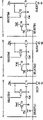
图3是表示根据本发明第一实施例的有机发光二极管器件的单元像素的电路框图。3 is a circuit block diagram showing a unit pixel of an organic light emitting diode device according to a first embodiment of the present invention.
图4是表示根据本发明第一实施例的对各个RGB像素施加了Vref电压的有机发光二极管器件的示例性视图。FIG. 4 is an exemplary view showing an organic light emitting diode device to which a Vref voltage is applied to respective RGB pixels according to a first embodiment of the present invention.
在根据本发明第一实施例的有机发光二极管器件中,沿第一方向形成选通线(未示出),并且沿与该第一方向交叉的第二方向以给定的间隔形成数据线(未示出)和电源线VDD由此形成一个像素区域。In the organic light emitting diode device according to the first embodiment of the present invention, gate lines (not shown) are formed along a first direction, and data lines (not shown) are formed at given intervals along a second direction crossing the first direction. not shown) and the power supply line V DD thus form a pixel area.
此外,第一开关薄膜晶体管TR2(寻址元件)与选通线GL和数据线DL交叉的区域相连。存储电容器(下文中,称为Cst)与第一开关薄膜晶体管TR2和电源线VDD相连。驱动薄膜晶体管TR1(电流源元件)与存储电容器Cst和电源线P相连,而有机发光二极管OLED与驱动薄膜晶体管TR1相连。In addition, the first switching thin film transistor TR2 (address element) is connected to a region where the gate line GL and the data line DL intersect. A storage capacitor (hereinafter, referred to as Cst) is connected to the first switching thin film transistor TR2 and the power supply line VDD. The driving thin film transistor TR1 (current source element) is connected to the storage capacitor Cst and the power supply line P, and the organic light emitting diode OLED is connected to the driving thin film transistor TR1.
此外,第二开关薄膜晶体管T3连接在第一开关薄膜晶体管T2与存储电容器Cst之间,第三开关薄膜晶体管T4连接在与存储电容器Cst相连的驱动薄膜晶体管T1的栅极和漏极之间,而第四开关薄膜晶体管T5连接在驱动薄膜晶体管T1和有机发光二极管OLED之间。In addition, the second switching TFT T3 is connected between the first switching TFT T2 and the storage capacitor Cst, and the third switching TFT T4 is connected between the gate and drain of the driving TFT T1 connected to the storage capacitor Cst, And the fourth switching thin film transistor T5 is connected between the driving thin film transistor T1 and the organic light emitting diode OLED.
这里,第三开关薄膜晶体管T4的栅极与第一开关薄膜晶体管T2相连,以耦接到SELECT(n)。Here, the gate of the third switching TFT T4 is connected to the first switching TFT T2 to be coupled to SELECT(n).
第二开关薄膜晶体管T3的栅极与第四开关薄膜晶体管T5的栅极相连,以耦接到EM(n)。The gate of the second switching TFT T3 is connected to the gate of the fourth switching TFT T5 to be coupled to EM(n).
第二开关薄膜晶体管T3的源极与可变电压Vref(为DC电压)相连。The source of the second switching thin film transistor T3 is connected to the variable voltage Vref (which is a DC voltage).
将参照图3和4来描述由此构造的根据本发明第一实施例的有机发光二极管器件的驱动电路和驱动方法。A driving circuit and a driving method of the thus constructed organic light emitting diode device according to the first embodiment of the present invention will be described with reference to FIGS. 3 and 4 .
参照图3,第一和第三开关薄膜晶体管T2和T4在SELECT(n)导通的部分C导通。Referring to FIG. 3, the first and third switching thin film transistors T2 and T4 are turned on at a portion C where SELECT(n) is turned on.
此时,将A节点电压初始化为VDD-|VTH|,并且B节点电压变为VDATA。At this time, the A node voltage is initialized to V DD −|V TH |, and the B node voltage becomes V DATA .
第二开关薄膜晶体管T3在SELECT(n)截止而EM(n)导通的部分D导通,由此使B节点电压变为可变电压Vref(为DC电压)。The second switching thin film transistor T3 is turned on at the portion D where SELECT(n) is turned off and EM(n) is turned on, so that the voltage of the B node becomes a variable voltage Vref (which is a DC voltage).
此时,A节点电压被提升(boost-rapping)了与B节点电压的变化率(VDATA-Vref)一样多,从而变为“VDD-|VTH|-VDATA-Vref”。At this time, the A node voltage is boosted (boost-rapping) as much as the change rate (V DATA −Vref) of the B node voltage, thereby becoming “V DD −|V TH |−V DATA −Vref”.
总结该结果,由以下表达式(2)来表示驱动薄膜晶体管T1的电流:Summarizing the results, the current driving the thin film transistor T1 is expressed by the following expression (2):
IOLEO=1/2K(|VGS|-|VTH|)2 I OLEO =1/2K(|V GS |-|V TH |) 2
=1/2K(VDD-VDD+|VTH|+VDATA-Vref-|VTH|)2 =1/2K(V DD -V DD +|V TH |+V DATA -Vref-|V TH |) 2
=1/2K(VDATA-Vref)2 (2)=1/2K(V DATA -Vref) 2 (2)
其中,K为u x Cox x W/L。Among them, K is u x Cox x W/L.
结果,电流IOLED变为VDATA和ref的函数。As a result, the current I OLED becomes a function of V DATA and ref.
因此,可以通过调节可变电压Vref来调节IOLED值,该可变电压Vref为用于对于一个帧保持存储在存储电容器Cst中的数据电压的DC电压。Accordingly, the I OLED value may be adjusted by adjusting the variable voltage Vref, which is a DC voltage for maintaining the data voltage stored in the storage capacitor Cst for one frame.
此外,如图4所述,可以通过下述的电路结构来调节色度和伽马值,在该电路结构中,对通过图3所述的电路结构而构成的各个RGB像素设置相应的可变电压Vref部分。In addition, as shown in FIG. 4, the chromaticity and gamma values can be adjusted through the following circuit structure. In this circuit structure, corresponding variable settings are set for each RGB pixel formed through the circuit structure described in FIG. voltage Vref part.
在这种情况下,与对产生电流的VDD进行调节的传统结构相比,可以更容易地应用不产生电流的Vref,并且可以对RGB有机发光二极管(OLED1、OLED2、OLED3)的特性的不均匀性进行补偿。In this case, Vref which does not generate current can be applied more easily than the conventional structure which adjusts V DD which generates current, and different characteristics of RGB organic light emitting diodes (OLED1, OLED2, OLED3) can be adjusted. Compensation for uniformity.
同时,将参照附图对根据第二实施例的有机发光二极管的驱动电路进行描述。Meanwhile, a driving circuit of an organic light emitting diode according to a second embodiment will be described with reference to the drawings.
图5是表示根据本发明第二实施例的有机发光二极管器件的单元像素的电路框图,其中与本发明的第一实施例一样,使用Vref以对于一个帧保持存储在Cst中的信息。5 is a circuit block diagram showing a unit pixel of an organic light emitting diode device according to a second embodiment of the present invention in which Vref is used to hold information stored in Cst for one frame as in the first embodiment of the present invention.
图6是表示根据本发明第二实施例的对各个RGB像素施加Vref电压的有机发光二极管的示例性视图。FIG. 6 is an exemplary view showing organic light emitting diodes applying a Vref voltage to respective RGB pixels according to a second embodiment of the present invention.
在根据本发明第二实施例的有机发光二极管器件中,沿第一方向形成选通线(未示出),并沿与该第一方向交叉的第二方向以给定的间隔形成数据线(未示出)和电源线VDD,由此形成一个像素区域。In the organic light emitting diode device according to the second embodiment of the present invention, gate lines (not shown) are formed along a first direction, and data lines (not shown) are formed at given intervals along a second direction crossing the first direction. not shown) and the power supply line V DD , thereby forming a pixel area.
此外,第二开关薄膜晶体管TR3(寻址元件)与选通线GL和数据线DL交叉的区域相连。存储电容器(下文中,称为Cst)与第二开关薄膜晶体管TR3和电源线VDD相连。驱动薄膜晶体管TR1(电流源元件)与存储电容器Cst和电源线P相连,而有机发光二极管OLED与驱动薄膜晶体管TR1相连。In addition, the second switching thin film transistor TR3 (address element) is connected to a region where the gate line GL and the data line DL intersect. The storage capacitor (hereinafter, referred to as Cst) is connected to the second switching thin film transistor TR3 and the power supply line V DD . The driving thin film transistor TR1 (current source element) is connected to the storage capacitor Cst and the power supply line P, and the organic light emitting diode OLED is connected to the driving thin film transistor TR1.
此外,第三开关薄膜晶体管T4连接在第二开关薄膜晶体管T3和存储电容器Cst之间,而第一开关薄膜晶体管T2连接在与存储电容器Cst相连的驱动薄膜晶体管T1的栅极和电源线VDD之间,由此将该栅极耦接到SELECT(n)。In addition, the third switching thin film transistor T4 is connected between the second switching thin film transistor T3 and the storage capacitor Cst, and the first switching thin film transistor T2 is connected between the gate of the driving thin film transistor T1 connected to the storage capacitor Cst and the power supply line V DD between, thereby coupling the gate to SELECT(n).
这里,第三开关薄膜晶体管T4连接在第二开关薄膜晶体管T3和存储电容器Cst之间,由此将其源极耦接到可变电压Vref(为DC电压)。与第一开关薄膜晶体管T2一样,第二开关薄膜晶体管T3的栅极连接到SELECT(n)。Here, the third switching thin film transistor T4 is connected between the second switching thin film transistor T3 and the storage capacitor Cst, thereby coupling its source to the variable voltage Vref (which is a DC voltage). Like the first switching TFT T2, the gate of the second switching TFT T3 is connected to SELECT(n).
此外,第三开关薄膜晶体管T4的栅极连接到EM(n)。In addition, the gate of the third switching thin film transistor T4 is connected to EM(n).
将参照图5和6描述由此构造的根据本发明第二实施例的有机发光二极管器件的驱动电路和驱动方法。A driving circuit and a driving method of the thus constructed organic light emitting diode device according to the second embodiment of the present invention will be described with reference to FIGS. 5 and 6 .
参照图5,第一和第三开关薄膜晶体管T2和T3在SELECT(n)导通的部分C导通。Referring to FIG. 5, the first and third switching thin film transistors T2 and T3 are turned on at a portion C where SELECT(n) is turned on.
此时,A节点电压被初始化为VDD,并且B节点电压变为VDATA。At this time, the A node voltage is initialized to V DD , and the B node voltage becomes V DATA .
第二开关薄膜晶体管T3在SELECT(n)截止而EM(n)导通的部分D导通,由此使B节点电压变为Vref电压。The second switching thin film transistor T3 is turned on at the portion D where SELECT(n) is turned off and EM(n) is turned on, so that the voltage of the node B becomes the voltage of Vref.
此时,A节点电压被提升了与B节点电压的变化率(VDATA-Vref)一样多,从而变为“VDD-|VTH|-VDATA-Vref”。At this time, the A node voltage is boosted as much as the change rate (V DATA -Vref) of the B node voltage, thus becoming "V DD -|V TH |-V DATA -Vref".
总结该结果,由以下表达式(2)来表示驱动薄膜晶体管T1的电流:Summarizing the results, the current driving the thin film transistor T1 is expressed by the following expression (2):
IOLED=1/2K(|VGS|-|VTH|)2 I OLED =1/2K(|V GS |-|V TH |) 2
=1/2K(VDD-VDD+VDATA-Vref-|VTH|)2 =1/2K(V DD -V DD +V DATA -Vref-|V TH |) 2
=1/2K(VDATA-Vref-|VTH|)2(2)=1/2K(V DATA -Vref-|V TH |) 2 (2)
其中,K为u x Cox x W/L。Among them, K is u x Cox x W/L.
根据该电流的表达式的结果,与第一实施例中一样,电流IOLED与可变电压Vref成比例,并且可以通过调节可变电压Vref来获得显示板之间的均匀亮度。From the result of the expression of this current, the current I OLED is proportional to the variable voltage Vref as in the first embodiment, and uniform luminance among display panels can be obtained by adjusting the variable voltage Vref.
此外,如图6所示,可以通过下述的电路结构来调节色度和伽马值,该电路结构使得对于通过图5所示的电路结构而构成的各个RGB像素,连接相应的可变电压Vref供给部分。In addition, as shown in FIG. 6, chromaticity and gamma values can be adjusted by a circuit structure such that for each RGB pixel formed by the circuit structure shown in FIG. 5, a corresponding variable voltage is connected Vref supply part.
同时,将参照附图描述根据第三实施例的有机发光二极管的驱动电路。Meanwhile, a driving circuit of an organic light emitting diode according to a third embodiment will be described with reference to the drawings.
图7是表示根据本发明第三实施例的有机发光二极管器件的单元像素的电路框图,其中示出了下述的情况:由于将n型p-Si TFT用作本发明第二实施例中的第三开关薄膜晶体管T4,所以不需要使用EM信号。7 is a circuit block diagram showing a unit pixel of an organic light emitting diode device according to a third embodiment of the present invention, which shows the following situation: Since an n-type p-Si TFT is used as a TFT in the second embodiment of the present invention The third switch thin film transistor T4, so there is no need to use EM signal.
图8是表示根据本发明第三实施例的对各个RGB像素施加了Vref电压的有机发光二极管器件的示例性视图。FIG. 8 is an exemplary view showing an organic light emitting diode device to which a Vref voltage is applied to each RGB pixel according to a third embodiment of the present invention.
在根据本发明第三实施例的有机发光二极管器件中,沿第一方向形成选通线(未示出),并沿与该第一方向交叉的第二方向以给定的间隔形成数据线(未示出)和电源线VDD,由此形成一个像素区域。In the organic light emitting diode device according to the third embodiment of the present invention, gate lines (not shown) are formed along a first direction, and data lines are formed at given intervals along a second direction crossing the first direction ( not shown) and the power supply line V DD , thereby forming a pixel area.
此外,第二开关薄膜晶体管TR3(寻址元件)与选通线GL和数据线DL交叉的区域相连。存储电容器(下文中,称为Cst)与第二开关薄膜晶体管TR3和电源线VDD相连。驱动薄膜晶体管TR1(电流源元件)与存储电容器Cst和电源线P相连,而有机发光二极管OLED与驱动薄膜晶体管TR1相连。In addition, the second switching thin film transistor TR3 (address element) is connected to a region where the gate line GL and the data line DL intersect. The storage capacitor (hereinafter, referred to as Cst) is connected to the second switching thin film transistor TR3 and the power supply line V DD . The driving thin film transistor TR1 (current source element) is connected to the storage capacitor Cst and the power supply line P, and the organic light emitting diode OLED is connected to the driving thin film transistor TR1.
此外,第三开关薄膜晶体管T4连接在第二开关薄膜晶体管T3和存储电容器Cst之间,并且第一开关薄膜晶体管T2连接在与存储电容器Cst相连的驱动薄膜晶体管T1的栅极和电源线VDD之间,由此耦接到SELECT(n)。In addition, the third switching thin film transistor T4 is connected between the second switching thin film transistor T3 and the storage capacitor Cst, and the first switching thin film transistor T2 is connected between the gate of the driving thin film transistor T1 connected to the storage capacitor Cst and the power supply line V DD Between, thus coupled to SELECT(n).
这里,第三开关薄膜晶体管T4连接在第二开关薄膜晶体管T3和存储电容器Cst之间,由此耦接到可变电压Vref(为DC电压)。与第一开关薄膜晶体管T2一样,第二开关薄膜晶体管T3的栅极和第三开关薄膜晶体管T4的栅极连接到SELECT(n)。Here, the third switching thin film transistor T4 is connected between the second switching thin film transistor T3 and the storage capacitor Cst, thereby being coupled to a variable voltage Vref (which is a DC voltage). Like the first switching TFT T2, the gates of the second switching TFT T3 and the third switching TFT T4 are connected to SELECT(n).
将参照图7和8描述由此构造的根据本发明第三实施例的有机发光二极管器件的驱动电路和驱动方法。A driving circuit and a driving method of the thus constructed organic light emitting diode device according to the third embodiment of the present invention will be described with reference to FIGS. 7 and 8 .
参照图7,第一和第三开关薄膜晶体管T2和T3在SELECT(n)变为低值的部分C导通。Referring to FIG. 7, the first and third switching thin film transistors T2 and T3 are turned on at a portion C where SELECT(n) becomes a low value.
当SELECT(n)从低值改变为高值时,第二开关薄膜晶体管T3截止,而第三开关薄膜晶体管T4导通,由此使B节点电压变为Vref电压。When SELECT(n) changes from a low value to a high value, the second switch thin film transistor T3 is turned off, and the third switch thin film transistor T4 is turned on, so that the voltage of the node B becomes Vref voltage.
此时,A节点电压被提升了与B节点电压的变化率(VDATA-Vref)一样多,从而变为“VDD-|VTH|-VDATA-Vref”。At this time, the A node voltage is boosted as much as the change rate (V DATA -Vref) of the B node voltage, thus becoming "V DD -|V TH |-V DATA -Vref".
总结该结果,由以下表达式(2)来表示驱动薄膜晶体管T1的电流:Summarizing the results, the current driving the thin film transistor T1 is expressed by the following expression (2):
IOLED=1/2K(|VGS|-|VTH|)2 I OLED =1/2K(|V GS |-|V TH |) 2
=1/2K(VDD-VDD+VDATA-Vref-|VTH|)2 =1/2K(V DD -V DD +V DATA -Vref-|V TH |) 2
=1/2K(VDATA-Vref-|VTH|)2(2)=1/2K(V DATA -Vref-|V TH |) 2 (2)
其中,K为u x Cox x W/L。Among them, K is u x Cox x W/L.
根据该电流的表达式的结果,与第二实施例中一样,电流IOLED与可变电压Vref成比例,并且可以通过调节可变电压Vref来获得显示板之间的均匀亮度。According to the result of the expression of this current, the current I OLED is proportional to the variable voltage Vref as in the second embodiment, and uniform luminance among display panels can be obtained by adjusting the variable voltage Vref.
此外,可以通过下述的电路结构来调节色度和伽马值,该电路结构使得对于各个RGB像素,连接相应的可变电压Vref供给部分。In addition, chromaticity and gamma values can be adjusted by a circuit configuration such that for each RGB pixel, a corresponding variable voltage Vref supply section is connected.
在这种情况下,与对产生电流的VDD进行调节的传统结构相比,可以更容易地应用不产生电流的Vref,并且可以对RGB有机发光二极管的特性的不均匀性进行补偿。In this case, Vref which does not generate current can be applied more easily compared to a conventional structure in which V DD which generates current is adjusted, and unevenness in characteristics of RGB OLEDs can be compensated for.
尽管在此根据优选实施例对本发明进行了描述,但是应该理解,对于本领域的技术人员,显然可以在不脱离本发明的主旨和范围的情况下进行多种变化。可以在不超出本发明以及以下所附权利要求的精神和范围的情况下,进行这些变化和修改。Although the invention has been described herein in terms of preferred embodiments, it should be understood that various changes would be apparent to those skilled in the art without departing from the spirit and scope of the invention. Such changes and modifications can be made without departing from the spirit and scope of the invention and the following appended claims.
Claims (14)
Applications Claiming Priority (2)
| Application Number | Priority Date | Filing Date | Title |
|---|---|---|---|
| KR1020040069348 | 2004-08-31 | ||
| KR1020040069348A KR101130903B1 (en) | 2004-08-31 | 2004-08-31 | Driving circuit of active matrix type organic light emitting diode device and method thereof |
Publications (2)
| Publication Number | Publication Date |
|---|---|
| CN1744180A CN1744180A (en) | 2006-03-08 |
| CN100583210C true CN100583210C (en) | 2010-01-20 |
Family
ID=36139527
Family Applications (1)
| Application Number | Title | Priority Date | Filing Date |
|---|---|---|---|
| CN200510082442A Expired - Lifetime CN100583210C (en) | 2004-08-31 | 2005-06-30 | Driving circuit and method for active matrix organic light emitting diode device |
Country Status (3)
| Country | Link |
|---|---|
| US (1) | US7545354B2 (en) |
| KR (1) | KR101130903B1 (en) |
| CN (1) | CN100583210C (en) |
Families Citing this family (38)
| Publication number | Priority date | Publication date | Assignee | Title |
|---|---|---|---|---|
| KR101152119B1 (en) * | 2005-02-07 | 2012-06-15 | 삼성전자주식회사 | Display device and driving method thereof |
| KR101186878B1 (en) * | 2005-08-26 | 2012-10-02 | 엘지디스플레이 주식회사 | VA mode LCD and driving method thereof |
| JP2007148222A (en) * | 2005-11-30 | 2007-06-14 | Hitachi Displays Ltd | Image display device |
| US7700471B2 (en) * | 2005-12-13 | 2010-04-20 | Versatilis | Methods of making semiconductor-based electronic devices on a wire and articles that can be made thereby |
| US7638416B2 (en) * | 2005-12-13 | 2009-12-29 | Versatilis Llc | Methods of making semiconductor-based electronic devices on a wire and articles that can be made using such devices |
| JP4887203B2 (en) | 2006-11-14 | 2012-02-29 | 三星モバイルディスプレイ株式會社 | Pixel, organic electroluminescent display device, and driving method of organic electroluminescent display device |
| KR101373736B1 (en) * | 2006-12-27 | 2014-03-14 | 삼성디스플레이 주식회사 | Display device and driving method thereof |
| JP2009109784A (en) * | 2007-10-31 | 2009-05-21 | Hitachi Displays Ltd | Image display device |
| KR100922071B1 (en) | 2008-03-10 | 2009-10-16 | 삼성모바일디스플레이주식회사 | Pixel and organic light emitting display device using same |
| KR101034690B1 (en) | 2009-09-02 | 2011-06-13 | 삼성모바일디스플레이주식회사 | Organic light emitting display device and driving method thereof |
| TWI433111B (en) * | 2010-12-22 | 2014-04-01 | Univ Nat Taiwan Science Tech | Pixel unit and display panel of organic light emitting diode containing the same |
| KR101813192B1 (en) * | 2011-05-31 | 2017-12-29 | 삼성디스플레이 주식회사 | Pixel, diplay device comprising the pixel and driving method of the diplay device |
| US9165518B2 (en) | 2011-08-08 | 2015-10-20 | Samsung Display Co., Ltd. | Display device and driving method thereof |
| US9019188B2 (en) | 2011-08-08 | 2015-04-28 | Samsung Display Co., Ltd. | Display device for varying different scan ratios for displaying moving and still images and a driving method thereof |
| CN103002624B (en) * | 2011-09-13 | 2015-02-25 | 昆山维信诺显示技术有限公司 | Active OLED (organic light emitting diode) lighting device |
| US9299301B2 (en) | 2011-11-04 | 2016-03-29 | Samsung Display Co., Ltd. | Display device and method for driving the display device |
| US9208736B2 (en) | 2011-11-28 | 2015-12-08 | Samsung Display Co., Ltd. | Display device and driving method thereof |
| CN102456319A (en) * | 2012-02-15 | 2012-05-16 | 福州华映视讯有限公司 | Pixel circuit and drive method for same |
| US9129572B2 (en) | 2012-02-21 | 2015-09-08 | Samsung Display Co., Ltd. | Display device and related method |
| JP6128738B2 (en) * | 2012-02-28 | 2017-05-17 | キヤノン株式会社 | Pixel circuit and driving method thereof |
| KR101360767B1 (en) * | 2012-08-17 | 2014-02-12 | 엘지디스플레이 주식회사 | Organic light emitting diode display device and method for driving the same |
| KR101391100B1 (en) * | 2013-01-18 | 2014-04-30 | 호서대학교 산학협력단 | Pixel circuit for driving oled |
| CN103236236A (en) * | 2013-04-24 | 2013-08-07 | 京东方科技集团股份有限公司 | Pixel driving circuit, array substrate and display device |
| US9620057B2 (en) | 2013-08-16 | 2017-04-11 | Boe Technology Group Co., Ltd. | Method and apparatus for adjusting driving voltage for pixel circuit, and display device |
| CN103559860B (en) * | 2013-08-16 | 2015-07-22 | 京东方科技集团股份有限公司 | Pixel circuit driving voltage adjusting method, pixel circuit driving voltage adjusting device, and display apparatus |
| CN104134427B (en) * | 2014-08-06 | 2016-08-24 | 友达光电股份有限公司 | pixel circuit |
| CN104575386B (en) * | 2015-01-26 | 2017-01-11 | 深圳市华星光电技术有限公司 | AMOLED pixel driving circuit and method |
| CN104599638A (en) * | 2015-02-12 | 2015-05-06 | 京东方科技集团股份有限公司 | Pixel circuit, drive method thereof and display device |
| CN105528996B (en) * | 2016-01-29 | 2018-04-10 | 深圳市华星光电技术有限公司 | Pixel compensation circuit, method, scan drive circuit and flat display apparatus |
| CN107274825B (en) | 2017-08-18 | 2020-11-24 | 上海天马微电子有限公司 | Display panel, display device, pixel driving circuit and control method thereof |
| CN109346012A (en) * | 2018-12-05 | 2019-02-15 | 深圳市华星光电半导体显示技术有限公司 | Pixel-driving circuit and display device |
| CA3141467A1 (en) * | 2019-05-29 | 2020-12-03 | Qing Li | Opto-electronic device fabrication method and electronic circuit |
| KR102760360B1 (en) | 2020-06-11 | 2025-02-04 | 삼성디스플레이 주식회사 | Pixel of an organic light emitting diode display device, and organic light emitting diode display device |
| KR20220138499A (en) | 2021-04-02 | 2022-10-13 | 삼성디스플레이 주식회사 | Display apparatus |
| KR102835171B1 (en) | 2021-09-24 | 2025-07-17 | 삼성디스플레이 주식회사 | Sweep signal driver and display device including the same |
| US11875755B2 (en) | 2022-01-14 | 2024-01-16 | Samsung Electronics Co., Ltd. | Method of driving light emitting diode backlight unit and display device performing the same |
| KR20240013951A (en) | 2022-07-21 | 2024-01-31 | 삼성디스플레이 주식회사 | Light emitting display device |
| KR20250067243A (en) | 2023-11-07 | 2025-05-15 | 삼성디스플레이 주식회사 | Pixel and display device including the same |
Family Cites Families (8)
| Publication number | Priority date | Publication date | Assignee | Title |
|---|---|---|---|---|
| GB0128419D0 (en) * | 2001-11-28 | 2002-01-16 | Koninkl Philips Electronics Nv | Electroluminescent display device |
| US7224333B2 (en) * | 2002-01-18 | 2007-05-29 | Semiconductor Energy Laboratory Co. Ltd. | Display device and driving method thereof |
| KR100469070B1 (en) * | 2002-02-19 | 2005-02-02 | 재단법인서울대학교산학협력재단 | Picture Element Structure of Active Matrix Organic Emitting Diode Display |
| KR100441530B1 (en) * | 2002-06-11 | 2004-07-23 | 삼성에스디아이 주식회사 | Display device of organic electro luminescent and driving method there of |
| KR100445435B1 (en) * | 2002-07-23 | 2004-08-21 | 삼성에스디아이 주식회사 | Display device of organic electro luminescent and driving method there of |
| JP4144462B2 (en) | 2002-08-30 | 2008-09-03 | セイコーエプソン株式会社 | Electro-optical device and electronic apparatus |
| KR100906964B1 (en) | 2002-09-25 | 2009-07-08 | 삼성전자주식회사 | Organic electroluminescent drive device and organic electroluminescent display panel having same |
| JP3832415B2 (en) * | 2002-10-11 | 2006-10-11 | ソニー株式会社 | Active matrix display device |
-
2004
- 2004-08-31 KR KR1020040069348A patent/KR101130903B1/en not_active Expired - Lifetime
-
2005
- 2005-06-30 CN CN200510082442A patent/CN100583210C/en not_active Expired - Lifetime
- 2005-06-30 US US11/172,479 patent/US7545354B2/en active Active
Also Published As
| Publication number | Publication date |
|---|---|
| KR101130903B1 (en) | 2012-03-28 |
| US20060043366A1 (en) | 2006-03-02 |
| US7545354B2 (en) | 2009-06-09 |
| KR20060020502A (en) | 2006-03-06 |
| CN1744180A (en) | 2006-03-08 |
Similar Documents
| Publication | Publication Date | Title |
|---|---|---|
| CN100583210C (en) | Driving circuit and method for active matrix organic light emitting diode device | |
| JP5135519B2 (en) | Organic electroluminescence display | |
| JP4477617B2 (en) | Organic light emitting diode display element and driving method thereof | |
| KR102664761B1 (en) | Organic light emitting diode display panel and display device thereof | |
| CN109979394B (en) | Pixel circuit and driving method thereof, array substrate and display device | |
| JP4914177B2 (en) | Organic light emitting diode display device and driving method thereof. | |
| KR100624137B1 (en) | Pixel circuit of organic electroluminescent display and driving method thereof | |
| CN101329836B (en) | Organic Light Emitting Diode Display Device | |
| KR101245218B1 (en) | Organic light emitting diode display | |
| KR101432126B1 (en) | Organic electroluminescent display device | |
| KR101117731B1 (en) | Pixel circuit, and organic light emitting display, and driving method thereof | |
| CN115691421A (en) | Pixel circuit, driving method thereof, array substrate and display device | |
| KR100635511B1 (en) | Organic electroluminescent display | |
| CN101986378A (en) | Pixel driving circuit for active organic light-emitting diode (OLED) display and driving method thereof | |
| JP2002258798A (en) | Electro luminescence panel | |
| WO2019165650A1 (en) | Amoled pixel driving circuit and driving method | |
| KR101288596B1 (en) | Organic Light Emitting Diode Display And Driving Method Thereof | |
| KR100646935B1 (en) | Light emitting display | |
| CN106128366B (en) | Pixel-driving circuit and its driving method and display device | |
| KR100583124B1 (en) | Light emitting display | |
| KR101153349B1 (en) | Organic Elecroluminescence Device and driving method of the same | |
| KR20060096857A (en) | Display device and driving method thereof | |
| KR20070071524A (en) | Method and apparatus for driving organic light emitting diode display device | |
| KR100741979B1 (en) | Pixel Circuit of Organic Electroluminescent Display | |
| KR101202041B1 (en) | Organic light emitting diode display and driving method thereof |
Legal Events
| Date | Code | Title | Description |
|---|---|---|---|
| C06 | Publication | ||
| PB01 | Publication | ||
| C10 | Entry into substantive examination | ||
| SE01 | Entry into force of request for substantive examination | ||
| C14 | Grant of patent or utility model | ||
| GR01 | Patent grant | ||
| CX01 | Expiry of patent term | ||
| CX01 | Expiry of patent term |
Granted publication date: 20100120 |